AMD A10-6700 And A10-6800K Review: Richland Hits The Desktop
Skip to main content
Tom’s Hardware is supported by its audience. When you purchase through links on our site, we may earn an affiliate commission. Here’s why you can trust us.
AMD’s Kabini: Jaguar And GCN Come Together In A 15 W APU showed us what the company’s Jaguar and GCN architectures could accomplish between 4 and 25 W TDPs. But, on the desktop, AMD isn’t quite ready to make the leap to a next-gen design. It just introduced its desktop-oriented Richland APUs, which aren’t really new at all. Rather, you can think of them as power-optimized Trinity parts, sporting the same Piledriver-based x86 cores and VLIW4 graphics configuration. Moreover, Richland-based APUs have been available to mobile device makers for months. The only real revelation is that we’re getting this update in the desktop and low-voltage mobile spaces now.
| Model | Radeon | Package | TDP | CPU Cores | Base/Max CPU Clock | L2 Cache | Radeon Cores | Base GPU Clock |
|---|---|---|---|---|---|---|---|---|
| A-Series Low-Voltage and Ultra Low-Voltage APUs | ||||||||
| A10-5745M | HD 8610G | FP2 | 25 W | 4 | 2. |
4 MB | 384 | 533 MHz |
| A8-5545M | HD 8510G | FP2 | 19 W | 4 | 1.7/2.7 GHz | 4 MB | 384 | 450 MHz |
| A6-5345M | HD 8410G | FP2 | 17 W | 2 | 2.2/2.8 GHz | 1 MB | 192 | 450 MHz |
| A4-5145M | HD 8310G | FP2 | 17 W | 2 | 2.0/2.6 GHz | 1 MB | 128 | 424 MHz |
In the table above, we see the new mobile-oriented options spanning 17 to 25 W TDPs. Richland isn’t much different from Trinity, but it’s more efficient thanks to specific Turbo Core optimizations that include a greater number of P-states to facilitate more granular power and performance levels.
| Model | Radeon | TDP | CPU Cores | Base/Max CPU Clock | Total Cache | Radeon Cores | GPU Clock | Unlock | Price |
|---|---|---|---|---|---|---|---|---|---|
| A10-6800K | HD 8670D | 100 W | 4 | 4. 1/4.4 GHz 1/4.4 GHz |
4 MB | 384 | 844 MHz | Yes | $149 |
| A10-6700 | HD 8670D | 65 W | 4 | 3.7/4.3 GHz | 4 MB | 384 | 844 MHz | No | $149 |
| A8-6600K | HD 8570D | 100 W | 4 | 3.9/4.2 GHz | 4 MB | 256 | 844 MHz | Yes | $119 |
| A8-6500 | HD 8570D | 65 W | 4 | 3.5/4.1 GHz | 4 MB | 256 | 800 MHz | No | $119 |
| A6-6400K | HD 8470D | 65 W | 2 | 3.9/4.1 GHz | 1 MB | 192 | 800 MHz | Yes | $77 |
And then we have the desktop-specific Richland parts. The very fastest model enjoys a 300 MHz base clock rate bump compared to the A10-5800K, along with official support for 2133 MT/s DDR3 memory (the other SKUs top out at 1866 MT/s memory). Also, its GPU is 44 MHz faster than the prior-gen version. And yet it fits within the same 100 W TDP.
On the other hand, the A10-6700 looks a lot like the -5800K, aside from a 100 MHz-lower base clock, a 100 MHz-higher Turbo Core ceiling, and a slightly quicker GPU. That one drops to a 65 W thermal limit.
Like the Trinity-based APUs before them, these Richland designs plug into a Socket FM2 interface. A BIOS update should be all that you need for compatibility with existing A55, A75, and A85 platforms.
And what about those shiny new Radeon model numbers? That’s marketing being bad. We were already dealing with Radeon HD 7000-series naming on APUs, which was confusing because AMD’s desktop 7000-series GPUs are commonly associated with the GCN architecture. Now we have 8000-series nomenclature. And yet, we’re still working with the VLIW4 configuration that was around back when AMD was shipping Radeon HD 6900-series cards. Architecturally, the only difference between Richland’s Radeon HD 8000 graphics and Trinity’s Radeon HD 7000 graphics is the name.
Again, the top-end A10-6800K gets 2133 MT/s memory support, which is particularly meaningful for its on-die graphics engine given a lack of shared L3 cache. The theoretical 34 GB/s of DDR3 bandwidth should go a long way to improve frame rates in the games we’ll be testing. With that said, let’s move on to why we aren’t able to test Richland’s Dual Graphics feature today…
- 1
Current page:
Richland APUs Make Their Way To The Desktop
Next Page AMD Dual Graphics: Not Ready For Benchmark Results
Topics
AMD
CPUs
Tom’s Hardware is part of Future US Inc, an international media group and leading digital publisher. Visit our corporate site .
©
Future US, Inc. Full 7th Floor, 130 West 42nd Street,
New York,
NY 10036.
AMD’s A10-6800K and A10-6700 ‘Richland’ APUs reviewed
AMD has had a rough time keeping up with Intel in the CPU market for the past couple of years. The firm’s Bulldozer CPU architecture hasn’t worked out as planned, and AMD has been forced to limit the scope of its ambition. Rather than competing with Intel across the entire market, it’s had to choose its battles, carefully positioning its products and seeking any possible seams in Intel’s armor. That strategy has succeeded in places, producing some potentially solid values for end users in the process.
When we reviewed the desktop version of AMD’s Trinity APUs last fall, the A10-5800K and A8-5600K, we found that they were a near-miss on the value front. The price was right compared to the competition. The CPU performance was good in some applications—those that use multiple threads well, like image processing tools or video encoders. And the integrated Radeon graphics simply outclassed what Intel had to offer in its Core i3.
But AMD was asking folks to accept some compromises in other areas. Single-threaded performance was relatively pokey, which could lead to reduced responsiveness in everyday tasks and momentary hiccups while gaming. More worryingly, the A10-5800K and A8-5600K chips consumed quite a bit more power than the competing Core i3—nearly twice as much at peak, 100W versus 55W. More power draw means more noise and heat, higher energy bills, and the need for larger PC enclosures.
In the end, that mix of advantages and drawbacks didn’t make a lot of sense to us. We just couldn’t envision many home-built PCs or pre-built systems where accepting a 100W power envelope to get somewhat better integrated graphics was a winning combination.
Just half a year later, AMD has refined the formula for its A-series processors under the umbrella of a new code name: Richland. Has the firm made enough progress to earn an unqualified win over the Core i3? We’ve done entirely too much testing in order to find out.
Trinity becomes Richland
Products based on Richland technology are distinct from the prior-generation Trinity parts, but not in the way you’d expect. Richland and Trinity share the same 32-nm silicon, with four integer cores, two floating-point units, and integrated Radeon graphics. On the desktop, they fit into the same Socket FM2-style motherboards.
Callout of the Trinity/Richland die. Source: AMD.
The differences have to do with the power management capabilities programmed into the chip’s firmware. Richland adds three big things that AMD simply didn’t have time to include in the first generation of products based on this chip. All of them have to do with dynamic behavior, how the APU’s onboard power management microcontroller directs the CPU and graphics cores to scale their clock speeds in response to different workloads.
First, AMD has spent more time in its labs characterizing what these chips can do—what clock frequencies they can tolerate and how much voltage they need to get there. Thus, Richland-based products have more operating points between their base and peak Turbo Core clock speeds. This finer-grained control should translate into higher efficiency, better performance, or both.
Second, Trinity contained an embedded network of temperature sensors across the chip, but those sensors weren’t used in determining how far Turbo Core could push on clock speeds. Instead, Trinity estimated its own power use by looking at activity counters. Because conditions vary in the real world, this method of estimating power use, and thus temperature, must rely on some fairly conservative assumptions. Richland’s rebuilt power management algorithm, called Hybrid Boost, takes direct input from the chip’s temperature sensors. Armed with better intelligence, Hybrid Boost can be more aggressive about pursuing higher clock speeds, giving Richland chips more frequency headroom.
Finally, AMD has added some smarts to Richland’s firmware that attempts to determine when one of the two major components of the chip, either the CPU or the integrated graphics processor (IGP), is the primary bottleneck in the current workload. For instance, if the IGP is the main holdup, Richland can rein in the CPU cores and shift more of its power budget to graphics in order to achieve better overall performance.
As you might imagine, all of this power-saving wizardry should have the most tangible benefits in laptops.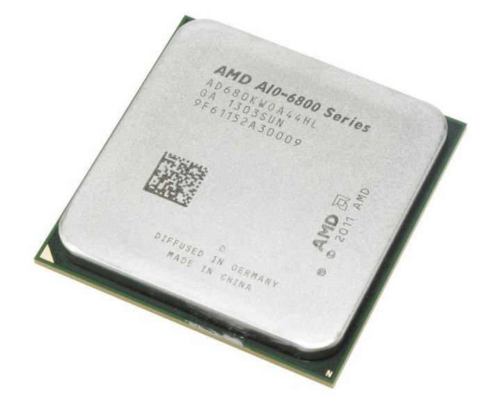 Still, Richland delivers some modest improvements on the desktop, as well. CPU base and Turbo frequencies have risen by 200-300MHz, and IGP speeds are between 40 and 84MHz higher, both within the same power envelope. The new A-series lineup looks like so:
| Model | Modules/
Integer cores |
Base core
clock speed |
Max Turbo
clock speed |
Total
L2 cache capacity |
IGP
ALUs |
IGP
clock |
TDP | Price |
| A10-6800K | 2/4 | 4.1 GHz | 4.4 GHz | 4 MB | 384 | 844 MHz | 100 W | $142 |
| A10-6700 | 2/4 | 3. 7 GHz 7 GHz |
4.3 GHz | 4 MB | 384 | 844 MHz | 65 W | $142 |
| A8-6600K | 2/4 | 3.9 GHz | 4.2 GHz | 4 MB | 256 | 844 MHz | 100 W | $112 |
| A8-6500 | 2/4 | 3.5 GHz | 4.1 GHz | 4 MB | 256 | 800 MHz | 65 W | $112 |
| A6-6400K | 1/2 | 3.9 GHz | 4.1 GHz | 1 MB | 192 | 800 MHz | 65 W | $69 |
The A10-6800K is the new flagship, and it sets the template. Compared to A10-5800K introduced last fall, the 6800K has a 300MHz faster base clock and a 200MHz higher Turbo peak. The IGP clock adds another 44MHz, too, while the max power (TDP) remains steady at 100W.
The model numbers that end in K, like 6800K, indicate unlocked parts whose multipliers can be raised at will for easy overclocking. Unlike Intel, AMD doesn’t delete features on its unlocked CPUs, so the 6800K still has all of its virtualization capabilities and advanced instruction support intact. Also, alone among the new Richland parts, the 6800K officially adds support for DDR3-2133 memory.
That said, perhaps the most eye-opening improvement over Trinity comes in the form of the A10-6700. Compared to the A10-5800, the 6700 has similar CPU clocks (100MHz lower base, 100MHz higher Turbo max) and a 44MHz faster IGP speed—and it manages that in a 65W power envelope, 35W less than the 5800K. That’s true progress, folks. Better yet, AMD has supplied us with an A10-6700 for testing, so we can see exactly how it matches up against the Core i3.
Special FX
We’ve also taken this opportunity to test some chips we’ve so far neglected: the lower-end models in AMD’s FX lineup. Like Richland, their CPU cores are based on the “Piledriver” microarchitecture. Beyond that, the two chips diverge. All of the FX models are based on a chip code-named Vishera, which natively has eight integer cores and, unlike the APUs, an 8MB L3 cache. Vishera doesn’t have integrated graphics or PCI Express, so it must rely on external chips (a discrete GPU and the 990FX chipset) to provide those capabilities. Naturally, then, the FX processors make use of a different CPU socket, dubbed Socket AM3+.
The fastest Vishera-based offering is the FX-8350, which we reviewed last year. AMD has since added a couple of cheaper options based on Vishera chips with portions disabled, the FX-6350 and FX-4350.
| Model | Modules/
Integer cores |
Base core
clock speed |
Max Turbo
clock speed |
L3
cache |
TDP | Price |
| FX-8350 | 4/8 | 4. 0 GHz 0 GHz |
4.2 GHz | 8 MB | 125 W | $195 |
| FX-6350 | 3/6 | 3.9 GHz | 4.2 GHz | 8 MB | 125 W | $132 |
| FX-4350 | 2/4 | 4.2 GHz | 4.3 GHz | 8 MB | 125 W | $122 |
These CPUs have similar clock speeds with varying core counts. From a computer-nerd standpoint, it’ll be interesting to see how these differences affect performance. Also from a computer-nerd standpoint, it’s a little disappointing to see that even the quad-core FX-4350 requires 125W to do its thing.
Happily, like the K-series Richland chips, all of these FX processors have unlocked multipliers without having any features disabled. They’re also fairly cheap. The six-core FX-6350 costs less than the quad-core A10-6800K.
You know, it wasn’t supposed to be this way. AMD’s CPU lineup is stacked closely together at fairly modest prices due to competitive pressure. Almost assuredly, the plan was for Socket FM2-based APUs to compete against Intel’s Ivy Bridge and Haswell quad-core CPUs with integrated graphics. The FX series, which is derived from server-class Opteron tech, would then go up against Intel’s high-end platform based on the X79 chipset, which is based on Xeon server tech. Instead, the eight-core FX-8350 sells for under $200, and everything else must cost less than that.
For now, the closest competition for the A10-6800K and A10-6700 is Intel’s Core i3-3225. That’s a 22-nm chip with dual cores, four hardware threads, a 3MB L3 cache, and Intel HD 4000 integrated graphics. The i3-3225 requires a bit less power than even the A10-6700, with a 55W TDP, and has a slightly lower list price of $134. That price also sets the Core i3 against the FX-6350, albeit in a much smaller power envelope. The Core i3-3225 is based on Intel’s older Ivy Bridge architecture; Haswell hasn’t quite made it into this price range yet, although it’s sure to get there eventually. When it does, Haswell should bring better graphics performance with it. For now, though, AMD has a bit of an opening. Let’s see how well Richland takes advantage of it.
Our testing methods
We ran every test at least three times and reported the median of the scores produced.
The test systems were configured like so:
| Processor | AMD FX-4350
AMD FX-6350 AMD |
AMD A10-5800K
AMD A10-6700 AMD A10-6800K |
| Motherboard | Asus Crosshair V Formula |
MSI FM2-A85XA-G65 |
| North bridge | 990FX | A85 FCH |
| South bridge | SB950 | |
| Memory size | 16 GB (2 DIMMs) | 16 GB (2 DIMMs) |
| Memory type | AMD Performance Series DDR3 SDRAM |
AMD Performance Edition DDR3 SDRAM |
| Memory speed | 1600 MT/s | 1600 MT/s |
| Memory timings | 9-9-9-24 1T |
9-9-9-24 1T |
| Chipset
drivers |
AMD chipset 13.  4 4 |
AMD chipset 13.4 |
| Audio | Integrated
SB950/ALC889 with Realtek 6.0.1.6873 drivers |
Integrated
A85/ALC892 with Realtek 6.0.1.6873 drivers |
| OpenCL ICD |
AMD APP 1124.2 |
AMD APP 1124.2 |
| IGP drivers |
– | Catalyst 13.5 beta 2 (Trinity) Catalyst 13.101 RC1 (Richland) |
| Processor | Core i3-3225
Core i5-3470 Core Core i7-3770K |
Core i7-4770K | Core i7-3970X |
| Motherboard | Asus P8Z77-V Pro |
Asus Z87-Pro |
P9X79 Deluxe |
| North bridge | Z77 Express |
Z87 Express |
X79 Express |
| South bridge | |||
| Memory size | 16 GB (2 DIMMs) | 16 GB (2 DIMMs) | 16 GB (4 DIMMs) |
| Memory type | Corsair
Vengeance Pro DDR3 SDRAM |
Corsair
Vengeance Pro DDR3 SDRAM |
Corsair
Vengeance DDR3 SDRAM |
| Memory speed | 1600 MT/s | 1600 MT/s | 1600 MT/s |
| Memory timings | 9-9-9-24 1T |
9-9-9-24 1T |
9-9-9-24 1T |
| Chipset
drivers |
INF update 9.  4.0.1017 4.0.1017
iRST 12.5.0.1066 |
INF update 9.4.0.1017 iRST 12.5.0.1066 |
INF update 9.4.0.1017 iRST 12.5.0.1066 |
| Audio | Integrated
Z77/ALC892 with Realtek 6.0.1.6873 drivers |
Integrated
Z87/ALC1150 with Realtek 6.0.1.6873 drivers |
Integrated
X79/ALC898 with Realtek 6.0.1.6873 drivers |
| OpenCL ICD |
Intel SDK for OpenCL 2013 |
Intel SDK for OpenCL 2013 |
Intel SDK for OpenCL 2013 |
| IGP drivers |
Intel 9.  18.10.3177 18.10.3177 |
Intel 9.18.10.3177 |
– |
They all shared the following common elements:
| Hard drive | Kingston HyperX Sh203S3 240GB SSD |
| Discrete graphics | XFX Radeon HD 7950 Double Dissipation 3GB with Catalyst 13.5 beta 2 drivers |
| OS | Windows 8 Pro |
| Power supply | Corsair AX650 |
Thanks to Corsair, XFX, Kingston, MSI, Asus, Gigabyte, Intel, and AMD for helping to outfit our test rigs with some of the finest hardware available. Thanks to Intel and AMD for providing the processors, as well, of course.
We used the following versions of our test applications:
- AIDA64 2.99.2446 beta
- Stream 5.8 64-bit
- SiSoft Sandra 2013.SP3a
- 7-Zip 9.20 64-bit
- TrueCrypt 7.1a
- Google Chrome 27.0.1453.94 m
- SunSpider 1.0
- The Panorama Factory 5.3 x64 Edition
- POV-Ray for Windows 3.7 RC7 64-bit
- Cinebench R11.5 64-bit Edition
- LuxMark 2.0
- x264 encoder r2334
- Handbrake 0.9.9 64-bit
- picCOLOR 4.0 build 786 64-bit
- Qtbench 0.2.2
- MyriMatch proteomics benchmark
- CASE Lab Euler3d CFD benchmark multithreaded edition
- Crysis 3
- Far Cry 3
- Tomb Raider
- GRID (2 pre-release)
- Metro: Last Light
- FRAPS 3.5.99
Some further notes on our testing methods:
- The test systems’ Windows desktops were set at 1920×1080 in 32-bit color. Vertical refresh sync (vsync) was disabled in the graphics driver control panel.
- We used a Yokogawa WT210 digital power meter to capture power use over a span of time. The meter reads power use at the wall socket, so it incorporates power use from the entire system—the CPU, motherboard, memory, graphics solution, hard drives, and anything else plugged into the power supply unit. (The monitor was plugged into a separate outlet.) We measured how each of our test systems used power across a set time period, during which time we encoded a video with x264.
- After consulting with our readers, we’ve decided to enable Windows’ “Balanced” power profile for the bulk of our desktop processor tests, which means power-saving features like SpeedStep and Cool’n’Quiet are operating. (In the past, we only enabled these features for power consumption testing.) Our spot checks demonstrated to us that, typically, there’s no performance penalty for enabling these features on today’s CPUs. If there is a real-world penalty to enabling these features, well, we think that’s worthy of inclusion in our measurements, since the vast majority of desktop processors these days will spend their lives with these features enabled.
The tests and methods we employ are usually publicly available and reproducible. If you have questions about our methods, hit our forums to talk with us about them.
Power consumption and efficiency
The workload for this test is encoding a video with x264, based on a command ripped straight from the x264 benchmark you’ll see later. We’re tracking power consumption over time in the first set of plots below. The main plot comes from our standard test systems with discrete Radeon graphics. The second one shows system-level power consumption with only the integrated graphics processors in use.
The story of progress from Trinity to Richland is told by comparing the green line on the plot for the A10-5800K with the blue-green line for the A10-6700. The A10-6700 consumes less power during the workload and finishes the job sooner, dropping back to idle before the 5800K does.
The Socket FM2 platform has nice, low power use at idle. The fact that a desktop system based on a full-sized ATX motherboard draws only 23-25W at the wall socket is remarkable.
Despite having a TDP rating of 65W, the A10-6700 system draws 48W more power while executing our test workload than our 55W Core i3-3225 system. In fact, it pulls more juice than a whole collection of configs based on Intel desktop CPUs with TDP ratings of 77W and 84W. At least the 6700 is a bit of an advance over AMD’s own A10-5800K.
We can quantify efficiency by looking at the amount of power used, in kilojoules, during the entirety of our test period, when the chips are busy and at idle.
Perhaps our best measure of CPU power efficiency is task energy: the amount of energy used while encoding our video. This measure rewards CPUs for finishing the job sooner, but it doesn’t account for power draw at idle.
If you compare the A10-6800K to the 5800K that precedes it, there’s only a sliver of difference between Trinity and Richland. Pit the A10-6700 against the 5800K, though, and the progress is a bit more pronounced. We’re happy to see the growth, but AMD will need to make much larger strides in order to catch up to Intel.
IGP performance: Tomb Raider
Next, we’ll move to gaming performance with integrated graphics. As usual, we’re testing games by measuring each frame of animation produced. The uninitiated can start here for an intro to our methods.
We’ve included a host of configurations in our IGP tests, building on what we did in our Haswell review. One of the entries, the Core i7-4950HQ, is a bit of a ringer; it uses an external 128MB eDRAM chip as a graphics cache, and it’s not a socketed processor. You can read more about it here. This time around, we have results for the 4950HQ running in a higher TDP mode of 55W, to see how it performs, because it’s an intriguing product. Intel tells us some PC makers will ship systems with this config. This CPU isn’t a direct competitor for the desktop versions of the A10. In fact, it’s priced to compete against a different version of the A10 that would be paired with a low-end discrete GPU.
The A10’s most direct competition is the Core i3-3225, of course. You’ll also want to keep an eye on the Core i7-4770K. The 4770K is a higher-end CPU, but it shares its Intel HD 4600 graphics with cheaper Haswell variants, down to the Core i5-4430 at $189. Eventually, the A10 will almost certainly have to compete directly with a lower-end CPU that includes HD 4600 graphics.
Oh, and we’ve tested several of the integrated graphics solutions with higher-clocked DDR3-2133 memory. The bandwidth available in a CPU socket is a major constraint for graphics performance, as the results will illustrate.
Although there are a few latency spikes in the frame time plots for all of the Radeon-based solutions, few of them amount to much in terms of absolute frame rendering times. (In fact, I’m pretty sure AMD is just batching up a few frames worth of work at once and dispatching it. That doesn’t appear to create any animation hiccups, so it must work with how this game engine advances the timing for its internal simulation of the game world.) The FPS average and our latency-focused metric, the 99th percentile frame time, tend to agree about the overall performance picture.
Compare the A10-6800K to the 5800K, and you’ll see that there’s very little daylight between them. In fact, the move to DDR-2133 memory makes more of a difference than the 44MHz gap between the two CPUs’ integrated graphics cores does. The A10-6700 doesn’t allow 2133MHz memory clocks, or it might be more impressive here. What it does do is essentially match the 5800K in our standard DDR3-1600 config.
Also, all of the AMD APUs outperform the Core i3-3225 by a very wide margin. The Haswell-based 4770K with HD 4600 graphics offers a much closer contest, though.
Practically speaking, the difference in animation smoothness between the A10 APUs and the Core i3 is bound to be huge. The i3-3325 is kind of a basket case when asked to run this game at these quality levels; over 13 seconds of our 60-second test are spent beyond our 50-ms threshold for frame rendering time. In other words, if you try to play Tomb Raider at these settings on the Core i3-3225’s IGP, you’re gonna have a bad time.
IGP performance: GRID 2
Forgive me for not having a video of this test session recorded. We just tested in the opening race of the game for 60 seconds.
GRID 2 shows us a little more progress from Trinity to Richland, but otherwise, the results are pretty similar to what we saw from Tomb Raider. AMD’s integrated graphics simply have the Core i3’s HD 4000 IGP outclassed. Haswell’s new HD 4600 edges closer to the 6700 and 6800K, but intermittent spikes in rendering times to nearly 80 ms mean that it doesn’t run this game as smoothly as Richland’s built-in Radeon.
IGP performance: Metro: Last Light
Latency-focused game testing is a lot of work, so I’ve thrown in this quick, automated test of Metro in order to give us another example of performance in a recent game. As you can see, there are few surprises given what we’ve already witnessed.
Crysis 3
Now we’ll turn our attention to gaming performance with a discrete graphics card.
Interesting. Although the FPS averages would appear to suggest strong performance from each of the CPUs, with only a small gap between them, the render time plots paint a more complex picture. Frame times spike pretty substantially at certain points the test run, and when they do, the slower CPUs with fewer cores tend to suffer. The 99th percentile frame time reflects this reality, showing a sizeable gap between the six-core FX-6350 and the quad-core FX-4350. With only two cores and four threads via Hyper-Threading, the Core i3-3225 is on the wrong side of this divide, as are all of the A10 APUs.
The FX-6350’s frame latencies are substantially lower than those of the A10, Core i3, and FX-4350 throughout the last 15-20% of frames rendered. I don’t think we’ve ever seen such clear evidence of a game making good use of more than four cores in a way that matters.
Far Cry 3
Look through all of the results above, and you’ll see a measurable advantage for the Core i3-3225 over the A10 APUs. However, the Core i3’s advantage is tiny. We’re talking two milliseconds in the 99th percentile frame time—and very little time spent working on frames that take longer than 50 milliseconds to render. Truth is, all of these CPUs run this game well.
Tomb Raider
Here’s another case of clear separation between the six-core FX-6350 and the quad-core FX-4350, Trinity, and Richland chips. The Core i3-3225 again has a slight advantage over the A10 APUs, too. All of these CPUs run this game quite competently, but the FX-6350 and the higher-end Intel CPUs sling out frames every 16.7 ms or less (that is, over 60 FPS) virtually no matter what.
Metro: Last Light
One last gaming test shows us a familiar pattern, with the i3-3225 just ahead of the A10 APUs.
Productivity
Compiling code in GCC
Our resident developer, Bruno Ferreira, helped put together this code compiling test. Qtbench tests the time required to compile the QT SDK using the GCC compiler. Here’s Bruno’s note about how he built it:
QT SDK 2010.05 – Windows, compiled via the included MinGW port of GCC 4.4.0.
Even though apparently at the time the Linux version had properly working and supported multithreaded compilation, the Windows version had to be somewhat hacked to achieve the same functionality, due to some batch file snafus.
After a working multithreaded compile was obtained (with the number of simultaneous jobs configurable), it was time to get the compile time down from 45m+ to a manageable level. This required severe hacking of the makefiles in order to strip the build down to a more streamlined version that preferably would still compile before hell froze over.
Then some more fiddling was required in order for the test to be flexible about the paths where it was located.
Which led to yet more Makefile mangling (the poor thing).
The number of jobs dispatched by the Qtbench script is configurable, and the compiler does some multithreading of its own, so we did some calibration testing to determine the optimal number of jobs for each CPU.
TrueCrypt disk encryption
TrueCrypt supports acceleration via Intel’s AES-NI instructions, so the encoding of the AES algorithm, in particular, should be very fast on the CPUs that support those instructions. We’ve also included results for another algorithm, Twofish, that isn’t accelerated via dedicated instructions.
7-Zip file compression and decompression
SunSpider JavaScript performance
Video encoding
x264 HD video encoding
We’ve devised a new x264 test, which involves one of the latest builds of the encoder with AVX2 and FMA support. To test, we encoded a one-minute, 1080p .m2ts video using the following options:
–profile high –preset medium –crf 18 –video-filter resize:1280,720 –force-cfr
The source video was obtained from a repository of stock videos on this website. We used the Samsung Earth from Above clip.
Handbrake HD video encoding
Our Handbrake test transcodes a two-and-a-half-minute 1080p H.264 source video into a smaller format defined by the program’s “iPhone & iPod Touch” preset.
Image processing
The Panorama Factory photo stitching
The Panorama Factory handles an increasingly popular image processing task: joining together multiple images to create a wide-aspect panorama. This task can require lots of memory and can be computationally intensive, so The Panorama Factory comes in a 64-bit version that’s widely multithreaded. I asked it to join four pictures, each eight megapixels, into a glorious panorama of the interior of Damage Labs.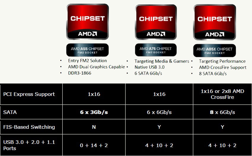
picCOLOR image processing and analysis
picCOLOR was created by Dr. Reinert H. G. Mueller of the FIBUS Institute. This isn’t Photoshop; picCOLOR’s image analysis capabilities can be used for scientific applications like particle flow analysis. Dr. Müller has supplied us with new revisions of his program for some time now, all the while optimizing picCOLOR for new advances in CPU technology, including SSE and AVX extensions, multiple cores, and Hyper-Threading. Many of its individual functions are multithreaded.
At our request, Dr. Müller graciously agreed to re-tool his picCOLOR benchmark to incorporate some real-world usage scenarios. As a result, we now have four tests that employ picCOLOR for image analysis: particle image velocimetry, real-time object tracking, a bar-code search, and label recognition and rotation. For the sake of brevity, we’ve included a single overall score for those real-world tests.
The AMD APUs perform well in our productivity suite, in part because these applications are nicely multithreaded, so the Trinity and Richland chips’ four integer cores are put to good use. The A10-6700 performs very much like the 5800K, and the 6800K is a bit quicker.
A couple of examples deserve some extra attention.
First, notice the Core i3-3225’s relatively abysmal performance in the TrueCrypt AES encryption test. That happens because, in this particular product, Intel has disabled the tailored instructions built into Ivy Bridge to accelerate AES encryption. AMD hasn’t played those games with its APUs, so they’re six to seven times faster at encrypting data with AES.
Second, the AMD chips make a relatively weak showing in SunSpider. This test is lightly multithreaded and involves a stacatto series of actions that takes place inside of a web browser. Intel’s CPU cores achieve much higher throughput in lighly multithreaded workloads like this one, and I think that’s worthy of note. For many day-to-day tasks, the Intel processors will be a little quicker and more responsive.
3D rendering
LuxMark
Because LuxMark uses OpenCL, we can use it to test both GPU and CPU performance—and even to compare performance across different processor types. OpenCL code is by nature parallelized and relies on a real-time compiler, so it should adapt well to new instructions. For instance, Intel and AMD offer integrated client drivers for OpenCL on x86 processors, and they both support AVX. The AMD APP driver even supports Bulldozer’s and Piledriver’s distinctive instructions, FMA4 and XOP. We’ve used the Intel ICD on the Intel processors and the AMD ICD on the AMD chips, since that was the fastest config in each case.
We’ll start with CPU-only results.
Now we’ll see how a Radeon HD 7950 performs when driven by each of these CPUs.
We can try combining the CPU and GPU computing power by asking both processor types to work on the same problem at once.
Now, let’s pull the discrete GPU out of the test systems and see how their IGPs perform in OpenCL.
Finally, we can use both the CPU cores and the IGPs working in concert.
You can see the promise of converged applications here. Look at the increase from the CPU-only test to the final CPU-plus-IGP result. Chips like Richland have the potential to employ their integrated graphics cores as a sort of super-FPU to tackle parallel computing problems like this one. AMD has talked a lot about that fact, but apparently two can play at this game. Intel’s Core i3 outperforms the AMD APUs in LuxMark.
Cinebench rendering
The Cinebench benchmark is based on Maxon’s Cinema 4D rendering engine. It’s multithreaded and comes with a 64-bit executable. This test runs with just a single thread and then with as many threads as CPU cores (or threads, in CPUs with multiple hardware threads per core) are available.
POV-Ray rendering
Scientific computing
MyriMatch proteomics
MyriMatch is intended for use in proteomics, or the large-scale study of protein. You can read more about it here.
STARS Euler3d computational fluid dynamics
Euler3D tackles the difficult problem of simulating fluid dynamics. Like MyriMatch, it tends to be very memory-bandwidth intensive. You can read more about it right here.
The Core i3 and the A10 APUs are pretty well matched through the rest of these benchmarks, which concentrate on the sorts of problems one would ideally want to tackle with a faster processor. Once again, take note of the AMD chips’ relatively weak performance in the single-threaded tests, including both Cinebench rendering and Euler3D fluid dynamics. The Core i3-3225 outperforms even the fastest AMD CPU on the market, the FX-8350, in those cases.
Overclocking
Since the 6800K has an unlocked multiplier, setting the multiplier to 48, upping the voltage a bit, and booting the system at 4.8GHz was incredibly simple. What came next was more complicated.
To test stability, I ran Prime95 and monitored temperatures with MSI ControlCenter software. The big tower cooler I installed on the 6800K easily kept temperatures in check; they never got higher than 59° C. However, the MSI software showed that, intermittently, CPU speeds were dropping down to 3.2GHz or so. Hmm.
I thought maybe the MSI monitoring software wasn’t reporting the CPU temperature correctly, but a quick series of finger tests on the CPU cooler and the motherboard VRM heatsinks told me that overheating was unlikely. After puzzling over it for a while, I noticed that the MSI motherboard was giving the 6800K quite a bit more voltage than requested. I had the BIOS set to 1.5V, and ControlCenter reported voltages as high as 1.608V. That’s a lot of juice, and I suspected that the motherboard was doing some throttling to keep the CPU from exceeding a power limit.
Sure enough, reducing the CPU voltage seemed to reduce the amount of throttling. I also set the BIOS option labeled “Core OCP Expander” to “Enhanced,” which seemed to help. Eventually, I found a stable config at 4.8GHz and 1.475V that produced only minor, occasional throttling in ControlCenter with Prime95 running. (Going below 1.475V led to lock-ups and blue screens.) The MSI board still ran the CPU voltage a little hot, reading as much at 1.576V under load, but CPU temperatures remained below 60° C. I figured I could run a few tests and see what my overclocking exploits had gained me.
Frustratingly, when I ran several benchmarks like Cinebench and x264 encoding, my overclocked 6800K appeared to be throttling more than expected. It was sometimes slower than the stock speed. 7-Zip fared a little better, but the performance gains weren’t terribly enthralling.
I suspect the A10-6800K could be overclocked further with a beefy water cooler, and either the right BIOS tweak or swapping in a different motherboard might help eliminate the throttling. Still, for the average guy looking to extract a little extra performance out of a CPU without too much extra expense, the 6800K doesn’t appear to have lots of easily accessible clock frequency headroom. Our sample doesn’t, at least.
Conclusions
Richland is a small step forward for AMD, as our ridiculous wealth of benchmark results has indicated. We can summarize things with a few of our famous value scatter plots, which mash up price with performance in several categories. As always, the better values will be closer to the top left corner of each plot.
The value scatter plots illustrate one of the strange things about Richland. The A10-6800K’s performance is a bit better than the older 5800K’s, and the new A10-6700 matches the 5800K within a smaller power envelope. Yet whichever one of these products you choose, AMD is asking an extra $20 for it. The price increase means these chips now cost more than the Core i3-3225, and it means Richland’s value proposition hasn’t really improved much from Trinity.
What AMD is offering you for $142 is better performance than the Core i3 in the sort of multithreaded applications that make up the bulk of our productivity suite, along with much nicer integrated graphics. The downside of this deal is that the A10 doesn’t perform as well in games when paired with a separate graphics card, in part because Intel’s individual CPU cores tend to be much more potent. Also, either version of the A10 burns quite a bit more power in real-world use than the Core i3-3225, regardless of how close the numbers in TDP specs might be. That will result in more heat and more noise than the competing Intel solution.
That said, I do think the A10-6700 seems like a more rational offering than the other Richland and Trinity parts we’ve encountered. I can see how a system builder—either a hobbyist or a big PC maker—putting together a basic system for a certain sort of user might like its mix of reasonably solid CPU performance, best-in-class integrated graphics, and a 65W power envelope. For the right system in a compact enclosure at a modest price, the A10-6700 could make more sense than the Core i3-3225. That’s more than I was able to say for the Trinity-based A10-5800K, which just didn’t seem to have a natural spot in the market.
Going forward, Intel apparently has plans to introduce Haswell-based Core i3s with HD 4600 graphics some time in the third quarter of this year. That will create a much tougher challenge for AMD’s APUs. Fortunately, before the year is out, AMD is slated to release an all-new replacement for Richland code-named “Kaveri.” That chip will feature the updated “Steamroller” CPU architecture and AMD’s excellent GCN graphics architecture. Who knows how the competitive picture will shape up once Haswell meets Kaveri? I suspect we’ll have an appropriately outsized collection of benchmarks to size things up when the time comes.
Gluttons for punishment can follow me on Twitter.
AMD A10-6800K (Richland) Review- Tech Reviews, Firstpost
AMD’s desktop APUs has been a budget DIYers dream solution since it has always delivered very good multimedia performance without having to invest in additional parts like a discrete GPU. Also, being an AMD component, the pricing has been very competitive when compared to the competition. This June, AMD launched their 2013 Elite A-Series APUs as a follow up to last year’s Trinity APUs. The new chips are more of a refresh to Trinity rather than a brand new architecture and now feature bumped up clock speeds, faster memory bandwidth and an upgraded GPU. Today we’ll be taking a closer look at their flagship A10-6800K APU which will eventually replace their, quite popular, A10-5800K Trinity APU.
Features
Before we delve into the nitty-gritty of what makes up the A10, here’s a quick look at the new line-up of APUs ranging from the A10 to the cheapest A6.
The new batch of Elite Series APUs
The APU consists of two or four ‘Piledriver’ CPU cores built on the 32nm fabrication process. The new APUs use the same FM2 socket so any A55, A75 or A85X motherboards are compatible with it. The new APUs have varied TDPs as well ranging from 65W to 100W. The A10-6500K that we’ll be reviewing today runs at a stock speed of 4.1GHz with the ability to Turbo up to 4. 4GHz. The APU has 2MB of L2 cache per dual-core module giving you a grand total of 4MB. The 6800K is the only APU currently in the family to natively support DDR3 2133MHz, which is quite impressive.
Offers a good blend of CPU and GPU performance
The Richland APUs feature a new Radeon HD 8000 graphics chip. These use the older VLIW 4 architecture first seen on AMD’s HD 6900 series desktop GPUs. The onboard graphics is pretty similar to the one on the 5800K APU and we have a total of 384 shaders, DX11 support and a slightly higher clock speed of 844MHz. The GPU and APU clock speeds can all be controlled via AMD’s Overdrive utility.
Setting it up
For setting up the A10-6800K, we turned to an MSI FM2-A85XA-G65. Based on the FM2 socket, this full-ATX motherboard supports memory up to 2133MHz (and beyond with OC), has a digital PWM and Military Class III components for good stability and supports CrossFire, AMD Dual Graphics and many more. Most importantly, the board worked very well out-of-the-box with the A10-6800K.
The MSI FM2-A85XA-G65 used for the test
Performance
The A10-6800K’s closest competitor in terms of price would be the Core i3-3240 or a Core i5-3330. Unfortunately, we couldn’t get those samples in so we’ll just have to make do with the higher-end Intel chips for now. While it’s not fair to directly compare them, we have an idea as to how much of a difference there is really.
|
Benchmarks |
||
|
|
AMD A10-6800K |
Intel Core i7-4770K |
|
PCMark 7 |
3257 |
4087 |
|
Cinebench R11.5 |
||
|
Open GL (FPS) |
58. |
96 |
|
CPU (PTS) |
3.44 |
7.8 |
|
7-zip (MIPS) |
3317 |
21048 |
|
Graysky’s X264 HD Benchmark v4.0 |
||
|
1st Pass (FPS) |
107 |
169 |
|
2nd Pass (FPS) |
22 |
48 |
As expected, the A10 finds it quite difficult to keep up with the likes of Intel latest Haswell or even Sandy Bridge for that matter. However, it’s not too far behind the 2600K when you look at the overall performance. The A10 may not have the computational prowess but when it comes to games, it still holds the lead. We have to say that Intel’s new HD 4600 graphics aboard Haswell is closing the gap so AMD might not have this lead for too long.
Still strong when it comes to gaming
Other than Resident Evil 5, the HD 4600 puts on a very good show giving us very playable framerates all around. The A10-6800K still manages to inch ahead thanks to a higher clock speed and better architecture.
Verdict and Price in India
The new Elite A-Series A10-6800K is priced a little higher than its predecessor at Rs 10,000. The A10 is targeted at someone who’s looking for a one-stop-solution for a CPU and GPU and would not want to invest more in a discrete card. Yes, you can get a more powerful Intel CPU at this price but you’ll have to spend at least Rs 3,000 more on a graphics card if you plan on even casual gaming. In this respect, the A10-6800K will be a slightly cheaper solution. If you already have a A10-5800K then upgrading to this won’t yield any noticeable performance increase. If it’s raw performance you crave then Intel’s Core i5-4430 (Haswell) is not out of reach and you also get a pretty decent onboard GPU for gaming.
Find latest and upcoming tech gadgets online on Tech3 Gadgets. Get technology news, gadgets reviews & ratings. Popular gadgets including laptop, tablet and mobile specifications, features, prices, comparison.
AMD A10-6800K and A10-6700 (Richland) Reviews
Written by
Matthew Lambert
June 5, 2013 | 07:52
Tags: #apu #core-i3 #core-i5 #fm2 #radeon-hd-8000 #richland #trinity #turbo-core
Companies: #amd
1 — AMD A10-6800K and A10-6700 (Richland) Reviews2 — AMD Richland — What’s New and Overclocking3 — Test Setup4 — AMD Richland — Cinebench and WPrime Performance5 — AMD Richland — Image Editing and Video Encoding Performance6 — AMD Richland — Multi-tasking and Overall Performance7 — AMD Richland — Gaming Performance8 — AMD Richland — Power Consumption9 — AMD Richland — Performance Analysis and Conclusion
Manufacturer: AMD
A10-6800K UK price (as reviewed):£114. 82 (inc VAT)
A10-6800K US price (as reviewed):$149.99 (ex Tax)
A10-6700 UK price (as reviewed):£114.80 (inc VAT)
A10-6700 US price (as reviewed):$148.99 (ex TAX)
In spite of Nvidia’s recent high end GPU launches, AMD’s range continues to remain competitive on this front, but its performance CPUs are sadly little match for Intel’s, with the recent release of Haswell further cementing the latter company’s lead in this arena. Its APUs are a different matter, however, as since the release of Llano, AMD has had a clear lead over Intel when it comes to onboard GPU performance, which Trinity subsequently improved upon. This has made the FM1 and FM2 platforms viable and attractive choices for budget builds where the power of a discrete GPU isn’t necessary, with APUs like the A10-5800K offering decent overall performance for a reasonable price. Indeed so compelling is the approach that famously both Microsoft and Sony have chosen AMD APUs to power their next generation consoles.
Click to enlarge
The recent reveal of AMD’s 2013 APU platforms demonstrated that the company is keen to focus much of its efforts on the mobile computing market. Temash, Kabini and the mobile Richland range placed much emphasis on low power consumption and increased performance-per-watt, traits which are somewhat more relevant in the world of notebooks, hybrids and tablets than in that of desktops. It’s easy to draw parallels with Haswell here too, as despite its desktop debut, the claimed significant improvements to power efficiency and onboard graphics will mainly be felt as Intel’s new architecture finds its way into the mobile space.
Nevertheless, it’s fair to say that neither AMD nor Intel has completely neglected desktop users, and today marks the launch of the non-mobile Richland APUs, with five new SKUs being made available immediately. Rather than a significant architectural overhaul, Richland is a relatively minor update to Trinity. As such, the new APUs are all based on socket FM2 and consequently supported by the exciting A-series chipsets, namely A55, A75 and A85x.
Depending on where you look, the price of the new APUs command roughly a 10 or 20 percent price premium over the corresponding Trinity parts, although AMD claims that Richland will sit alongside Trinity in its FM2 range rather than outright replacing it.
Today we’re testing the two top models of the range, the A10-6800K and the A10-6700. They can both be found for £110, which makes them around £20 dearer than the Intel Core i3-3220, the most recent budget CPU we’ve had the opportunity to look at.
| APU Model | A10-6800K | A10-6700 | A8-6600K | A8-6500 | A6-6400K |
| GPU | HD 8670D | HD 8670D | HD 8570D | HD 8570D | HD 8470D |
| TDP | 100W | 65W | 100W | 65W | 65W |
| GPU Cores | 384 | 384 | 256 | 256 | 192 |
| GPU Clock Speed | 844 MHz | 844 MHz | 844 MHz | 800 MHz | 800 MHz |
| CPU Cores | 4 | 4 | 4 | 4 | 2 |
| CPU Clock (Turbo/Base) GHz | 4. |
4.3/3.7 | 4.2/3.9 | 4.1/3.5 | 4.1/3.9 |
| Total L2 Cache | 4MB | 4MB | 4MB | 4MB | 1MB |
| Max DDR3 | 2133 | 1866 | 1866 | 1866 | 1866 |
| AMD Turbo Core | Yes | Yes | Yes | Yes | Yes |
| Unlocked Multiplier | Yes | No | Yes | No | Yes |
| RRP | £116.99 | £116.99 | £91.99 | £91.99 | £57.95 |
At a high level, there’s little that’s changed between Trinity and Richland, as both sets of desktop APUs are based on Piledriver cores, built with 32nm technology and rated with TDPs of 65-100W. The Radeon 7000 series’ onboard graphics component has been newly christened as the Radeon 8000 series, but in this instance both are fundamentally the same thing. As before, the GPU’s memory is tied to the system memory, so faster memory kits should mean higher frame rates.
As AMD has stuck with the same 32nm manufacturing process and the same form factor and die size as before, there’s quite literally little room for physical improvements. Thus, one of the most obvious areas for increasing performance is that of clock speeds, and indeed both the CPU and GPU clocks have been given a bump. The A10-6800K and A10-6700 have had their GPU clock speed increased by 5.5 percent compared to the A10-5800K and A10-5700, while the base CPU clock has been upped by about 8 and 9 percent respectively. Hopefully these higher clock speeds haven’t impacted on the chip’s overclocking potential, which you can read about over the page.
1 — AMD A10-6800K and A10-6700 (Richland) Reviews2 — AMD Richland — What’s New and Overclocking3 — Test Setup4 — AMD Richland — Cinebench and WPrime Performance5 — AMD Richland — Image Editing and Video Encoding Performance6 — AMD Richland — Multi-tasking and Overall Performance7 — AMD Richland — Gaming Performance8 — AMD Richland — Power Consumption9 — AMD Richland — Performance Analysis and Conclusion
AMD A10-6800K Quad-Core A10-Series Black Editi AD680KWOHLBOX B&H
BH #AMA106800K • MFR #AD680KWOHLBOX
Key Features
- Designed for Desktop Computers
- Base Speed Frequency Is 4.
1 GHz
- Power-Efficient Quad-Core Architecture
- Single Chip Supports Both CPU & GPU
The AMD A10-6800K Quad-Core A10-Series Black Edition Accelerated Processor with Radeon HD 8670D Graphics combines a quad-core processor and discrete HD graphics on a single, power-effiecient chip that enables energy-efficient performance with low power consumption. This model is designed for desktop computers and its four cores support a 4.1 GHz base speed frequency. The processor has a total of 4MB L2 Cache, a DDR3-2133 memory interface, and it supports DirectX Version 11.
More Details
No Longer Available
Share
PrintAsk Our Experts
-
Overview
-
Specs
-
Reviews0
-
Q&A
- Accessories
AMD A10-6800K Overview
The AMD A10-6800K Quad-Core A10-Series Black Edition Accelerated Processor with Radeon HD 8670D Graphics combines a quad-core processor and discrete HD graphics on a single, power-effiecient chip that enables energy-efficient performance with low power consumption. This model is designed for desktop computers and its four cores support a 4.1 GHz base speed frequency. The processor has a total of 4MB L2 Cache, a DDR3-2133 memory interface, and it supports DirectX Version 11.
In the Box
- AMD A10-6800K Quad-Core A10-Series Black Edition Accelerated Processor with Radeon HD 8670D Graphics
- Limited 3-Year Warranty
AMD A10-6800K Specs
| Series | AMD Quad-Core A10-Series Black Edition APU |
| Compatibility | Desktop Computers |
| Processor Cores | 4 |
| Graphics Card | AMD Radeon HD 8670D (discrete) |
| Frequency | 4. |
| L2 Cache Count | 4 |
| L2 Cache | 1024 KB (4 MB total) |
| CMOS | 32 nm |
| Memory Interface | DDR3-2133 |
| Wattage | 100 W |
| Socket | FM2 |
| DirectX Version Support | 11 |
| Maximum Temperature | 165°F (74°C) |
| Dimensions | Not specified by manufacturer |
| Weight | Not specified by manufacturer |
Packaging Info
| Package Weight | 0. |
| Box Dimensions (LxWxH) | 4.5 x 3.4 x 2.4″ |
AMD A10-6800K Reviews
See any errors on this page? Let us know
YOUR RECENTLY VIEWED ITEMS
AMD Richland A10-6800K AND A10-6700 Review
Victor Wu
June 4, 2013
AMD, CPU/Processors, Hardware, Reviews & Articles
2 Comments
Not letting Intel grab all of the spotlight, AMD has officially released the desktop version of the upgraded Trinity APU codenamed Richland. While Richland does not bring any architectural change over the Trinity, AMD is able to deliver a decent amount of performance improvements by tuning the existing chip. We have got the top of the line A10-6800K and a 65W A10-6700 in our lab that we will put through our tests.
For a budget desktop computer, the AMD APU certainly offers plenty of horse-power. Since the introduction of the first generation APU in 2011, AMD has kept a yearly cycle of releasing a new APU. In January 2011, “Llano” integrated the K10 CPU microarchitecture with AMD VLIW5 GPU. It also integrated the Northbridge, PCI Express, and DDR3 memory controller. The second generation “Trinity” released a year ago gets an upgrade on the CPU to the Piledriver cores that is based on the module design of two integer cluster and one floating point unit. Toward the end of this year, we should expect the Kaveri come to the market that brings both CPU and GPU upgrade with the Streamroller CPU core and the GCN graphic core.
|
Year |
Codename |
Process |
Die transistor |
Socket |
CPU |
GPU |
|
June 2011 |
Llano |
32 nm SOI |
228 mm2/ 1. |
FM1 |
K10 |
HD 6000 (VLIW5) |
|
Oct 2012 |
Trinity |
32 nm SOI |
246 mm2/ 1.303 billion |
FM2 |
Piledriver |
HD 7000 (VLIW4) |
|
June 2013 |
Richland |
32 nm SOI |
246 mm2/ 1.303 billion |
FM2 |
Piledriver |
HD 8000 (VLIW4) |
AMD is making one more push of the Piledriver based APU before we can get our taste of the Kaveri. The Richland can be consider as the 2.5 generation APU as it bears no major architectural change over the Trinity that we have reviewed (AMD Virgo Platform or Trinity Integrated GPU performance) last year. . However, AMD has made some refinement on the Richland to deliver a more balanced performance out of its APUs.
The Richland incorporate temperature sensors on the chip to provide more accurate calculation of the of the APU power consumption which allows it to further fine-tuning the frequency and voltage plot to optimize the efficiency of the chip. Additionally, the power consumption can be better managed so that it can throttle the CPU or the GPU appropriately depending on the workload. As a result, AMD is able to improve upon the performance of its existing chip by balancing the workloads between the CPU and the GPU.
|
Model |
TDP (W) |
cores |
Freq/Turbo |
GPU |
Freq |
Radeon Cores |
|
A10-6800K* |
100 |
4 |
4. |
HD 8670D |
844 |
384 |
|
A10-6700 |
65 |
4 |
3.7/4.3 |
HD 8670D |
844 |
384 |
|
A10-5800K |
100 |
4 |
3.8/4.2 |
HD 7660D |
800 |
384 |
|
A10-5700 |
65 |
4 |
3.4/4.0 |
HD 7660D |
760 |
384 |
|
A8-6600K |
100 |
4 |
3. |
HD 8570D |
844 |
256 |
|
A8-6500 |
65 |
4 |
3.5/4.1 |
HD 8570D |
800 |
256 |
|
A8-5600K |
100 |
4 |
3.6/3.9 |
HD 7560D |
760 |
256 |
|
A8-5500 |
65 |
4 |
3.2/3.7 |
HD 7560D |
760 |
256 |
|
A8-5400K |
65 |
2 |
3. |
HD 7540D |
760 |
192 |
|
A6-6400K |
65 |
2 |
3.9/4.1 |
HD 8470D |
800 |
192 |
|
A4—5300 |
65 |
2 |
3.4/3.6 |
HD 7480D |
724 |
128 |
The fastest 100W A10-6800K APU gets a boot of 300 MHz in the CPU clockspeed (200 MHz Turbo) or 8%. The GPU also gets 5.5% boost to 844 MHz. The number of cores on both the CPU and Radeon cores on the GPU remained the same as the A8-5800K. The memory speed also gets a boots where the new A10-6800K supports DDR3-2133MHz, up from the 1866MHz.
AMD also launched a 65W A10-6700 that is clocked at 100MHz higher on the CPU and 44MHz higher on the GPU than the A8-5800K. This APU should offer the performance of the A8-5800K but consumes much less power which makes it even more competitive against the Intel Core i3 processors.
The Richland APUs will carry the 6000 numbering system and will come in 65W and 100W TDP models. Despite the same GPU architecture as the Trinity, AMD has rebranded the GPU on the Richland to HD 8000. Generally speaking, expect the similar numbered Richland APU to have 200~300 MHz speed bump on the CPU and 5~10% bump on the GPU.
While there is no major architectural change on Richland, AMD has improved upon the the power management of the APU. Today’s CPUs/APUs feature an intricate power management algorithm that throttles the clockspeed for the CPU and GPU according to the type of workloads. Under light workloads that do not utilize all of the cores, there is thermal headroom to allow the APUs/CPUs to run at a higher clockspeed than its base clock. For AMD, this is called Turbo Core.
With Trinity, AMD’s implementation of the Turbo Core technology is based on the power consumption of the CPU or the GPU. Based on the workload, the chip will translate the power consumption into thermal temperature and if there is a thermal headroom available, the CPU or the GPU will get a speed bump. AMD has fine-tuned its algorithm with Richland by incorporating real-time, power based temperature calculation with the data coming off the various sensors placed inside the chip. AMD call this “Hybrid Boost”. By combining the power consumption and the on-die temperature sensor, AMD is able to further refine the frequency and power plot and add additional operational point that the chip is able to throttle.
Again, throttling will work on both the CPU and the GPU. According to AMD, the new algorithm will deliver more balanced performance by detecting if a CPU or a GPU is bottlenecked and shifting power appropriately to ensure the most optimal performance.
Richland supports all of the current instruction sets that includes SSE 4.2, FMA 4/3, AES, XOP. It will work with the existing FM2 socket motherboards, though you may need a quick BIOS update before the board will recognize the APU. Current FM2 motherboard using A85X A75, and A55 chipset that offers SATA 6 Gbps and USB 3.0. While they are not up to the same level in terms of performance as Intel’s offering, they are nonetheless up to date. The only thing that is missing with the Richland is the support for PCI Express 3.0. Considering that this is aimed at budget/mainstream build we really do not think that anyone would missed out on the extra bandwidth provided by the PCI Express.
This year, AMD is also pushing Wireless Display with its APU. AMD’s Wireless Display is based on the Miracast standard. Unlike Intel’s offering that requires Intel based Wireless card, AMD’s solution will work with Broadcomm or Atheros Wireless card. We were not provided with a list of compatible cards nor we receive a unit to test with our sample. Based on the information provided, it appears that the option to enable the Wireless Display is built in the AMD Catalyst Display Driver that can easily be enabled if you have one of the compatible wireless card and the display.
AMD positions the desktop APU (Richland and the Trinity) against the Intel Core i3 processors. The top of the line A10-6800K is even going against some of the entry level Core i5 processors with its stronger GPU power. The Trinity APU already is quite competitive against the Core i3 thanks to the Turbo and we do expect the A10-6800K to even narrow the gap between the two.
| Test Rig | |
| Case | Open Air |
| CPUs |
Intel: Intel Core i7 3770K (Ivy Bridge – LGA 1155 -Z77) Intel Core i5 2500K Intel Core i3 2100 AMD: A10-5800K A10-5600K A10-6800K A10-6700 A8-3870K FX-8350 |
| Motherboards |
Intel: Socket 1155: Gigabyte Z77X-UD3H AMD FM2: Asus F2A85V PRO FM1: Gigabyte A75-UD4H AM3+: Asus Crosshair V Formula |
| Ram |
Kingston HyperX Gray 4 GB (2x2GB) G. |
| CPU Cooler |
Zalman CNPS9900 Max Thermalright SI-128 |
| Hard Drives |
Seagate Barracuda XT 3TB |
| SSD | 1x OCZ Vertex 3 240GB SATA III 6Gb/s SSD |
AIDA64 V2.60
The extra speed bump on the A10-6800K gives us about 2~5% gain in the performance. The A10-6700 performance is going to be depended on the type of workload since the APU is clocked at lower speed than the A10-5800K but it is able to Turbo up to 100MHz higher. So for lightly threaded tasks, it performs faster than the A10-5800K but heavy threaded workloads favors the A10-5800K.
We are taking a slightly different approach with the PCMark 7 benchmark. We decided to assess the overall system performance with just the integrated GPU only so that we can get a sense on how well the system performs if you are just using the IGP for common tasks. While PCMark is a synthetic benchmark, it does provide us an overview of how well the AMD APU scales up and how it compares against the Intel’s offering.
AMD positioned the APU against the Intel Core i3 processor and based on the PCMark, we can see that it is rightfully so. AMD is also positioning the top model, the A10-6800K, against the entry level Core i5 based on its GPU performance. The A10-6700 edges out the A10-5800K here probably due to the combination of its higher GPU clockspeed and higher Turbo speed.
When comes to content creation, Intel Core i5 is still faster but the A10-6800K shows a 25% gain over the A10-5800K.
PCMark productivity benchmark gives us 2% additional performance on the A10-6800K over the A10-5800K.
Intel Core i3 processor has an advantage of higher instruction per clock (IPC) which helps out with the lightweight tasks. Here we can see that the A10-6800K is just barely faster than the Sandy Bridge Core i3 2100.
The computation benchmark shows us that there is 80% improvement on the A10-6800K.
The A10-6800K does rather well here with 25% improvement over the A10-5800K.
We get 6.8% improvement in the single thread performance on the A10-6800K compare and 2% for the A10-6700 compare to the A10-5800K. The A10-6800K is still lagging quite a lot behind the Intel processors which we hope that AMD can address with Kaveri or at least narrow the gap significantly.
For the multi-thread, we also get 6% improvement for the A10-6800K. The A10-6700 performs just a tad under the A10-5800K. The A10-6800K is able to further push ahead of the Core i3 2100 in the multi-threaded workloads.
Interestingly, the A10-6700 is about 4% slower than the A10-5800K in the OpenGL benchmark. Given to the fact that both APUs have the same numbers of Radeon Cores but the A10-6700 is clocked at higher speed, we would expect it to come on top. We think the lower lower TDP and AMD’s own power management may have played a role here to result in a lower performance.
TrueCrypt 7.1
Data encryption is is one of the strength for the AMD APU since Intel Core i3 CPU lacks the hardware support. We do not know if Intel plans to bring such support to the entry level CPUs but if data encryption is critical to you, the AMD APU is certainly going to give you a significant performance improvement with its hardware encryption support. While AMD APUs are not as fast as what Intel has to offer with its Core i5 and Core i7’s hardware encryption, it is nonetheless faster than those processors lacking such support by as much as three times.
Gaming
We have already know that the AMD APU has a faster integrated GPU than the Intel HD 4000 found in the Ivy Bridge. The additional clockspeed on the A10-6800K should push its performance even further ahead. The Haswell Iris Pro graphics with the embedded eRAM is going to improve the performance but that only applies to high-end models. Currently, Intel has not released budget Core i3 Haswell based processors so we do not know how the APU will fare against the Haswell based APU. We toss in the Core i7 3770K into the mix because it comes with the fastest graphics on the current Ivy Bridge Core i3 processor from Intel. Here we also tested the A10-6800K at its default 1866MH speed and 2133 MHz. We decided to skip the performance with a discreet card here since we expect the result to mimic what we have observed with the Trinity plus a few percentage improvements.
Richland yields about 3% improvement over the Trinity and with DDR3-2133MHz, we get about 6% gain in the overall score from 3DMark11.
Same result can be observed with the graphics test in the 3Dmark 11.
The A10-6800K actually is able to deliver 30 FPS here. So it is possible to play game like Metro 2033 with the A10-6800K at 1680×1050 medium setting. We see that at 2133MHz, we gained about 10% performance.
We get 3% improvement here with the A10-6800K and about 5% running the memory at 2133MHz with the Lost Planet 2 and the Alien vs Predator.
Media Encoding
Cyberlink MediaExpresso 6.5 supports the Intel Quick Sync and AMD VCE. When comes to video transcoding, nothing can touch Intel’s QuickSync at the moment. The A10-6800 and the A10-6700 is just as fast as the A10-5800K. This is not too surprising considering that the workload is done via the GPU and all three APUs have the same number of Radeon cores and the additional clockspeed is probably not going to have major impact for this type of workloads..
HandBrake: OpenCL Performance
HandBrake is an open source media converter that supports OpenCL. The software is available online free to download but the current version 0.9.9 does not yet support the OpenCL and we have gotten a beta version that allows us to test the performance with OpenCL. Despite the OpenCL support, the AMD A10-6800K still lags behind the Intel Core i5 2500K.
x264 HD v4.0
No major surprise here as we see the A10-6800K gained about 10% in performance.
About 5% gain here, making it almost as fast as the Phenom II X4 980. If you are still clinging to the old quad-core socket AM3 processor, maybe it is time to upgrade to the new platform as you know that you will get equal or better performance at lower power consumption.
The new revision of x264 benchmark puts a greater demand on the processing power and we will start to incorporate this benchmark result in the future. Here we added the Core i3 2100 as a comparison to see just how well the APU fares against Intel’s entry offering. Both the A10-6700 and the A10-6800K performs rather well here. The A10-6800K is about 20% faster than the Core i3 2100.
Compute Power: OpenCL
One area where AMD is relying heavily on its APU is the GPU compute power. When the first APU is launched the list of software that supports OpenCL is very limited. Two years later, the list is still not as big as we hoped but we are at least glad to see it is growing. Looking at the chart above and we can see that many of the professional and some of the commonly used applications are already supporting OpenCL.
We picked two benchmarks, Luxmark and the Rightware Basemark, to assess the APU’s OpenCL performance.
LuxMark v2.0
Greater emphasize has been put on the OpenCL support. Now that Intel has the OpenCL support on the Ivy Bridge and the Haswell, we should see a greater software vendors to add such support to their codes.We turn to the Luxmark v2.0 to get a sense on the total computing power of the chip.
Starting off, we take a look at just the CPU performance. As expected, the APU is not match for Intel’s offering.
Moving to the GPU performance, we can see that AMD has about three times of the advantage. We include the Intel Core i7 3770K here since it is the fastest GPU on any Ivy Bridge processor. Intel has yet to release the Haswell based Core i3 so we do not know its performance.
Putting both the CPU and GPU together, we see the A10-6700 is actually about 10% slower than the A10-5800K. This is a bit unexpected as we see the CPU on the A10-6700 is 5% slower but its GPU is 3.6% faster. We kind of expect the performance to be somewhat event out or at lest not that big of a different. Looks like AMD’s new Turbo algorithm may play some role here at shifting the power between the CPU and GPU.
Rightware Basemark
The Rightware Basemark is another benchmark that incorporate the OpenCL support. Here AMD dominated the chart.
Looking at the individual benchmarks and it is clear that has advantage here except the Physics test.
Power Consumption, Temperature and Overclocking
Power Consumption
Keep in mind that the power consumption is dependent on the platform as opposed to just the CPU alone. With both Intel and AMD producing not just the CPU but also the chipset, both companies are able to more tightly regulate the chip in order to minimize power leakage.
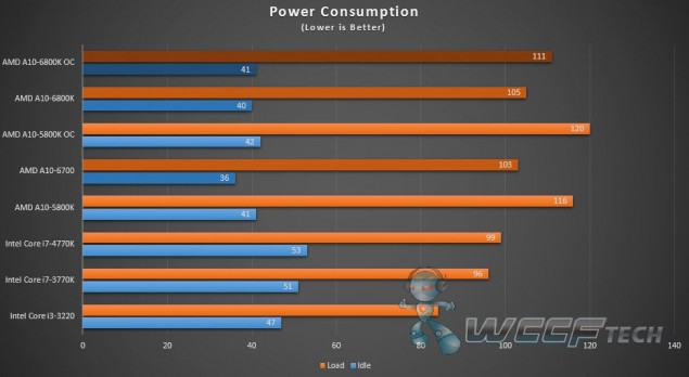
Looks like AMD is able to shed off couple of wattage of power from the Richland APU. Idle we see the A10-6800K consumes 45 watts of power, which is 2 watts fewer than the A10-5800K
Under load, it consumes 146 watts of power. The power consumption is still higher than Intel’s Core i3 and Core i5 processor. The A10-6700 is much more manageable at 124 watts under load, which is lower than even the Core i3 2100.
Temperature
Idle, the new APU’s temperature is similar to the Trinity based APU at 30°C.
Under load, the temperate is also consistent with the older APU at manageable 52°C with our SI-128 heatsink. The core temperature of the A10-6800K dropped a couple of degree. The A10-6700 load temperature is at 45°C, just 1 °C higher than the Intel Core i3 2100.
Overclocking
Previously, we were not unable to overclock the A10-5800K beyond 4.5GHz so we kind of known how far we can push on the A10-6800K. Given to the fact that the A10-6800K is already clocked at higher speed, we do not expect we can push it too far from the 4. 1GHz stock speed. We were able to push the APU to 4.6GHz easily by simply raising the multiplier on the processor in the BIOS, so the overclocking result is pretty much identical between the Richland and the Trinity.
We could actually get the APU to run at 4.7GHz without any trouble. It will crash Prime95 but the system remains stable and no lock up. We noticed that at this speed, the CPU core temp reached alarming 111ºC and CPU temp reached 60ºC and the power consumption reached to 207 watts, or 50 more watts than the stock speed. It is very likely that there are still room for overclocking if you are going with water-cooling or more extreme cooling solution.
Conclusion
The A10-6800K delivers somewhere from 5% to 25% performance improvements over the A10-5800K where a workload is CPU bound, then the improvement often lies on the lower end of the spectrum. On the average, the APU is about 10% faster than its predecessor. There is just so much you can do with the additional clockspeed without architectural modification or redesign. It is still rather impressive to see about 10% improvements without any architectural change. Hopefully with Kaveri will bring a sizable gain in the CPU performance.
The launch of Richland is not a game changer for AMD and no one expects it to be so. It still does what it does the best, ie any workloads that can tap into the integrated GPU such as gaming. Of course, if you are using a dedicated graphic card, then you may not care much about the IGP. On the CPU front, it is certainly a capable processor and is capable of delivery good performance at its price point.
AMD positions the APU against the Intel Core i3 since the performance is almost a toss up between the two. The Core i3 obviously wins in the light workloads but the APU has strength in certain heavier workloads and the GPU power. AMD also has additional arsenal in its disposal with the inclusion of the AES support and the ability to pair with a relative budget GPU for added performance. AMD has small window to grab some market shares since Intel has not yet announced the Core i3 parts based on the Haswell architecture so it is currently going against the Ivy Bridge or the Sandy Bridge Core i3. Based on what we can gather, even if Intel’s upcoming Core i3 CPU is able to deliver about 25% to 50% improvement over the current HD 4000 GPU, AMD may still has a slight edge but we have to reserve the judgment until we get a chance to test it
It is a bit difficult for us to recommend upgrading to the FM2 platform if you are currently using the FM1 socket platform since we know very well that in a few months, we will get to see Kaveri. AMD has not officially come out and say if the upcoming platform will support FM2 socket. Rumors floating around the web is that the upcoming APU will use the FM2+ socket which at the moment, we do not know if this means that potentially some current motherboard may support Kaveri with a bios update. It is possible we may see the same story like AM3/AM3+ upgrade where older socket may support the newer CPU minus a few features. Our recommendation is that unless you absolutely need a new platform now, then wait for Kaveri.
If you are currently using a dual-core FM2 system, upgrading to the A10-6800K is certainly not a bad upgrade to prolong the lifespan for a couple of more years for $100. Or if you are looking to upgrade three or four years old PC, the FM2 platform is certainly a very good alternative to the Intel Core i3 platform. Not only that you get a much more powerful system, the IO upgrade to SATA 6Gbps and USB 3.0 are certainly going to make world difference. The FM2 platform is also a great choice if you are building a media PC as well, especially the 65W A10-6700. Even for a budget system, the A10-6800K is certainly more than capable of playing games and the money saved can very well be put into a better graphic cards or an SSD which in term should offer a much greater performance improvements.
AMD A10-6800K processor review and testing GECID.com. Page 1
::>Processors
>2013
> AMD A10-6800K
11-09-2013
Page 1
Page 2
One page
At one time, AMD made a real splash in the market of computer components by introducing a new concept of processors — APU or Accelerated Processing Unit. APU is a crystal that houses both the processor part and the graphics part, with the latter playing a very large role. Of course, integrated graphics technology is not new and has been used for a long time, but it was AMD that brought this concept to a new level, as users now have the opportunity to run modern games without buying an external video card, albeit at medium / minimum settings.
Therefore, it is not surprising that the manufacturer is trying to push the concept of APU on the market, and sometimes even too fast. Last October, the company introduced the world to the second generation of APUs, codenamed AMD Trinity. And even a year has not passed, and new models have already appeared on the market, in the name of which the word “APU” appears again. This time the family was called AMD Richland . We will get acquainted with it in this review, and on the example of the flagship processor model — AMD A10-6800K .
But before proceeding directly to the description and testing of new items, let’s see how AMD Richland APUs differ from AMD Trinity APUs. And, alas, as it is not regrettable to say, but practically nothing. No, of course, some improvements were made, but in a cardinal sense, nothing much has changed. AMD Richland APUs are still manufactured on the 32nm process, with a die area of 246 sq. mm and the number of transistors is about 1.3 billion.
And you don’t need to be a great expert in the field of processor engineering to understand what we are talking about. Just look at these two pictures. As the saying goes: «Find ten differences.»
Photo of the Crystal of the Family processor AMD Trinity
Family Crystal AMD 9000 9000 9000 9000 9000 9000 9000 9000 9000 9000 9000 9000 9000 9000 9000 9000 9000 9000 9000 9000 all the same, the so-called dual-core modules, each of which contains two computing devices capable of processing two data streams simultaneously. The integrated graphics core has not changed either, it still occupies almost half of the die (42% to be exact) and uses exactly the same VLIW4 architecture. The increase in performance was achieved by increasing the clock frequency of the video core. We will talk about this in more detail a little later, when we consider the AMD Richland APU lineup.
What really deserves attention is the memory controller. Now in the older model (AMD A10-6800K) it officially supports DDR3 memory modules operating at 2133 MHz (in the AMD Trinity APU this value was limited to 1866 MHz). Recall that it is the memory speed that is the «bottleneck» in systems with integrated graphics.
Other features include an improvement in the Turbo Core mode, as well as a change in the load balance between the CPU and GPU for hardware video encoding and decoding.
Now for something more pleasant. AMD Richland APUs are fully compatible with boards based on the Socket FM2 platform. And we are talking about the processor socket and chipsets (AMD A55/A75/A85X). Therefore, the upgrade for owners of computers based on AMD Trinity processors will be painless. It will be enough just to update the BIOS firmware.
And, of course, the proprietary technologies AMD Dual Graphics and AMD Eyefinity have not gone away. Recall that the first (AMD Dual Graphics) allows you to combine the capabilities of the graphics core integrated into the processor and a discrete video card. The second (AMD Eyefinity) allows you to connect up to four monitors and take full advantage of the interface of the MS Windows 8 operating system.
Summing up, we can say that in the face of the AMD Richland APU, we received an improved version of the AMD Trinity APU, so to speak, «AMD Trinity 2.0». Although you have to give credit to the manufacturer. AMD did not mislead users and immediately after the release of the AMD Trinity APU, described the approximate capabilities of the AMD Richland APU. At the same time, it was emphasized that more global changes will occur in the third generation of APUs, code-named AMD Kaveri. But let’s not get ahead of ourselves, AMD Kaveri APUs will not appear until 2014, so let’s take a closer look at the AMD Richland APU lineup.
Model range
At the moment, the AMD Richland processor series is represented by only five models. As in the case of AMD Trinity APUs, the manufacturer divided the new hybrid solutions into classes depending on their performance:
|
Model APU |
A10-6800K |
A10-6700 |
A8-6600K |
A8-6500 |
A6-6400K |
|
Graphics core |
HD 8670D |
HD 8670D |
HD 8570D |
HD 8570D |
HD 8470D |
|
Thermal package (TDP), W |
100 |
65 |
100 |
65 |
65 |
|
Number of processor cores |
4 |
4 |
4 |
4 |
2 |
|
Processor frequency (base/Turbo Core), GHz |
4. |
3.7/4.3 |
3.9/4.2 |
3.5/4.1 |
3.9/4.1 |
|
Number of shaders |
384 |
384 |
256 |
256 |
192 |
|
Graphics core frequency, MHz |
844 |
844 |
844 |
800 |
800 |
|
Level 2 cache (L2), MB |
4 |
4 |
4 |
4 |
1 |
|
Maximum speed of supported DDR3 memory, MHz |
2133 |
1866 |
1866 |
1866 |
1866 |
This table allows us to understand why AMD Richland APUs should be more productive than their predecessors. Although the conclusion suggested itself in the previous part of the article — if the architecture has not changed, then the clock frequencies must be increased, which we see in practice. Depending on the model, the AMD Richland APU frequency increased by 100 — 500 MHz. If we talk about the Turbo Core mode, then there is also an increase in approximately the same range of 200 — 400 MHz.
The speed of the graphics part has increased by 40 — 44 MHz. Note that the number of shader pipelines has not changed either up or down.
Processors with index «K» have an unlocked multiplier, due to which they have the possibility of overclocking. Support for DDR3-2133 MHz memory modules by the «top» model AMD A10-6800K has already been mentioned above.
This diagram shows how AMD sees second generation APUs in the desktop. That is, you need to understand that the AMD Richland family of processors did not come to replace AMD Trinity, but as an addition to it, thereby significantly expanding the range of APUs for the Socket FM2 platform.
Also, let’s not forget that after the release of full-fledged AMD Richland APUs, their analogues with a disabled video core will definitely appear on the market. So far, they have not been officially presented, but some information about such specimens pops up on the pages of various foreign resources. We have already published a relevant note in the news section. According to it, the AMD Richland APU range will expand with five more processors with a locked graphics core — AMD Sempron 250, AMD Athlon X2 350, AMD Athlon X4 750, AMD Athlon X2 370K and Athlon X4 760K.
From AMD’s side, this is a very correct move. After all, in this way the company itself will profit from the sale of «unsuccessful» instances, and users will be able to purchase processors at a lower price. Recall that APUs with a disabled core are usually cheaper and have a very good price / performance ratio.
Appearance and packaging
And now let’s move from theory to practice and take a closer look at the flagship model of the AMD Richland APU generation — AMD A10-6800K . An OEM sample or a tray version of the processor came to our test lab, so there is no description of the packaging and cooling system. Let’s move on to the appearance of the APU itself.
Externally, the processor is absolutely no different from its predecessor, made for the Socket FM2 platform. On the heat-distributing cover there is a marking and the name of the country of manufacture, in this case China. Although the processor got there already for the final assembly. The crystal itself was grown in Germany, as indicated by the inscription «Diffused in Germany».
Since all AMD Richland APUs are compatible with Socket FM2, it is not surprising that there is no difference between the backs of AMD A10-6800K and, for example, AMD A10-5800K.
Specification
|
Model |
AMD A10-6800K |
|
Marking |
AD680KWOA44HL |
|
Processor socket |
Socket FM2 |
|
Clock frequency (nominal), MHz |
4100 |
|
Maximum clock speed with Turbo Core 3. |
4400 |
|
Multiplier |
41 |
|
Bus frequency, MHz |
100 |
|
L1 cache size, KB |
2 x 64 (instruction memory) 4 x 16 (data memory) |
|
L2 cache size, KB |
2 x 2048 |
|
L3 cache size, KB |
No |
|
Microarchitecture |
Piledriver |
|
Core |
Richland |
|
Number of cores/threads |
4/4 |
|
Instruction support |
MMX(+), SSE, SSE2, SSE3, SSSE3, SSE4, SSE4A, SSE4.1, SSE4.2, x86-64, AMD-V, AES, AVX, XOP, FMA3, FMA4 |
|
Supply voltage, V |
0. |
|
Power dissipation, W |
100 |
|
Critical temperature, °C |
74 |
|
Process |
32 nm |
|
Technology Support |
Dual Graphics UVD3 Turbo Core 3.0 PowerNow! Eyefinity |
|
Built-in memory controller |
|
|
Maximum memory size, GB |
64 |
|
Memory types |
DDR3 (up to 2133 MHz) |
|
Number of memory channels |
2 |
|
Integrated Radeon HD 8670D |
|
|
Stream Processors |
384 |
|
SIMD |
6 |
|
Texture blocks |
24 |
|
Rasterization modules |
8 |
|
GPU clock frequency, MHz |
844 |
|
Instruction support |
DirectX 11 OpenGL 4. DirectCompute 11 OpenCL 1.1 |
All prices for AMD+A10-6800K
The CPU-Z program confirms the information written above in the table. As can be seen from the screenshot, in normal operation (Turbo Core 3.0 technology is disabled), the clock speed of the AMD A10-6800K is 4100 MHz, with a bus speed of 100 MHz and a multiplier of «x41». At the time of reading, the core voltage was 1.296 V.
If you use the dynamic overclocking mode or simply the “automatic overclocking” function using proprietary Turbo Core 3.0 technology, the multiplier is increased by two points to the value “x43”. At the same time, the processor speed increases to 4300 MHz, and the voltage to 1.448 V. Many readers will probably wonder why the specification indicates that the speed in turbo mode is 4400 MHz, while in fact the frequency was only 4300 MHz. This is precisely the improvement in the work of Turbo Core 3.0 technology. When under load, the AMD A10-6800K runs at 4.3GHz most of the time. If not all processor cores are loaded with work, the frequency can rise to a maximum of 4.4 GHz.
In idle mode, the multiplier is reduced to the value «x20», thus — the frequency is up to 2000 MHz. The voltage is 0.888 V.
The AMD A10-6800K cache is distributed similarly to the «top» processors from the AMD Trinity APU family. L1 cache: 16 KB for each of the 4 cores is allocated for data with 4 associativity channels, while there are 64 KB for the instruction for each dual-core module (remember, there are two in a quad-core processor) with 2 channels associativity. L2 cache: 2 MB per dual-core processor module with 16 channels of associativity. There is no L3 cache.
The DDR3 memory controller operates in dual channel mode and supports RAM up to 2133 MHz.
Graphics core specification is fully confirmed by GPU-Z utility. As we said above, the AMD Radeon HD 8670D has 384 shader units and runs at 844 MHz.
And before proceeding directly to testing, let’s take a look at the comparative table of the main technical characteristics of the new flagship AMD A10-6800K and its predecessor — AMD A10-5800K.
|
Model |
AMD A10-6800K |
AMD A10-5800K |
|
Processor frequency (base/Turbo Core), GHz |
4.1/4.4 |
3.8/4.2 |
|
Number of processor cores |
4 |
4 |
|
Level 2 cache (L2), MB |
4 |
4 |
|
Thermal package (TDP), W |
100 |
100 |
|
Number of shaders |
384 |
384 |
|
Graphics core frequency, MHz |
844 |
800 |
|
Maximum speed of supported DDR3 memory, MHz |
2133 |
1866 |
Review of the AMD A10-6800K processor: specifications, benchmark tests
The A10-6800K processor was released by AMD, release date: June 4, 2013. At the time of release, the processor cost $142. The processor is designed for desktop computers and is based on the Richland architecture.
Processor unlocked for overclocking. The total number of cores is 4, threads are 4. The maximum clock speed of the processor is 4.4 GHz. The maximum temperature is 74°C. Technological process — 32 nm SOI. Cache size: L1 — 192 KB, L2 — 4 MB.
Supported memory type: DDR3.
Supported socket type: FM2. The maximum number of processors in the configuration is 1. Power consumption (TDP): 100 Watt.
AMD Radeon HD 8670D graphics are integrated into the processor with the following graphics parameters: maximum frequency — 844 MHz, number of cores — 384.
| Top1 CPU |
| This CPU |
CPU mark
| Top1 CPU |
| This CPU |
| 118142 |
Single Core
| Top1 CPU |
| This CPU |
Multi-Core
| Top1 CPU |
| This CPU |
Face Detection
| Top1 CPU |
| This CPU |
| 56.680 mPixels/s |
| 4.893 mPixels/s |
Ocean Surface Simulation
| Top1 CPU |
| This CPU |
| 741.453 Frames/s |
| 10.547 Frames/s |
T-Rex
| Top1 CPU |
| This CPU |
| 3. |
| 0.209 Frames/s |
Video Composition
| Top1 CPU |
| This CPU |
| 49.002 Frames/s |
| 0.604 Frames/s |
Bitcoin Mining
| Top1 CPU |
| This CPU |
| 218.231 mHash/s |
| 3. |
Car Chase Offscreen
| Top1 CPU |
| This CPU |
| 9047 Frames |
| 1267 Frames |
Manhattan
| Top1 CPU |
| This CPU |
| 7128 Frames |
| 4136 Frames |
T-Rex
| Top1 CPU |
| This CPU |
| 12887 Frames |
| 4604 Frames |
Car Chase Offscreen
| Top1 CPU |
| This CPU |
| 9047.000 Fps |
| 1267.000 Fps |
Manhattan
| Top1 CPU |
| This CPU |
| 7128. |
| 4136.000 Fps |
T-Rex
| Top1 CPU |
| This CPU |
| 12887.000 Fps |
| 4604.000 Fps |
| Name | Value |
|---|---|
| PassMark — Single thread mark | 1601 |
| PassMark — CPU mark | 3165 |
| Geekbench 4 — Single Core | 542 |
| Geekbench 4 — Multi-Core | 1494 |
| CompuBench 1. |
4.893 mPixels/s |
| CompuBench 1.5 Desktop — Ocean Surface Simulation | 10.547 Frames/s |
| CompuBench 1.5 Desktop — T-Rex | 0.209 Frames/s |
| CompuBench 1.5 Desktop — Video Composition | 0.604 Frames/s |
| CompuBench 1.5 Desktop — Bitcoin Mining | 3.801 mHash/s |
| GFXBench 4.0 — Car Chase Offscreen | 1267 Frames |
| GFXBench 4.0 — Manhattan | 4136 Frames |
| GFXBench 4.0 — T-Rex | 4604 Frames |
| GFXBench 4. |
1267.000 Fps |
| GFXBench 4.0 — Manhattan | 4136.000 Fps |
| GFXBench 4.0 — T-Rex | 4604.000 Fps |
| Core frequency | 844MHz |
| Process | 32 nm |
| Number of shaders | 384 |
Gaming performance
1. The Witcher 3 (2015)
2. GTA V (2015)
3. X-Plane 10.25 (2013)
4. Battlefield 4 (2013)
5. Total War: Rome II (2013)
6 Company of Heroes 2 (2013)
7. Metro: Last Light (2013)
8 BioShock Infinite (2013)
9. StarCraft II: Heart of the Swarm (2013)
10. SimCity (2013)
11. Tomb Raider (2013)
12 Crysis 3 (2013)
13 Hitman: Absolution (2012)
14. Call of Duty: Black Ops 2 (2012)
15. Diablo III (2012)
16. The Elder Scrolls V: Skyrim (2011)
17. Battlefield 3 (2011)
18. Quake 3 Arena — Timedemo (1999)
The Witcher 3 (2015)
| Low, 1024×768 | 21.20 |
GTA V (2015)
| Low, 1024×768 | 50. |
| Medium, 1366×768 | 42.00 |
| High, 1920×1080 | 14.60 |
| Ultra, 1920×1080 | 5.80 |
X-Plane 10.25 (2013)
| Low, 1024×768 | 60.10 |
| Medium 1366×768 | 29.40 |
| High, 1366×768 | 12.10 |
| Ultra, 1920×1080 | |
| Low, 1024×768 | 52.40 |
| Medium, 1366×768 | 37.00 |
| High, 1366×768 | 23.60 |
| Ultra, 1920×1080 | 7.90 |
Total War: Rome II (2013)
| LOW, 1024×768 | 65.00 |
| Medium, 1366×768 | 48.70 |
| HIGH, 1366×768 | |
| Ultra, 1920×1080 | 7. |
Company of Heroes 2 (2013)
| Low, 1024×768 | 27.20 |
| Medium, 1366×768 | 22.10 |
| High, 1366×768 | 11.70109 |
| Medium, 1366×768 | 29.70 |
| High, 1366×768 | 14.80 |
| Ultra, 1920×1080 | 7.60 |
BioShock Infinite (2013)
| Low, 1280×720 | 76.50 |
| Medium, 1366×768 | 39.60 |
| HIGH, 1366×768 | 33.10 |
| Ultra, 1920×1080 | 9 |
StarCraft II: Heart of the Swarm (2013)
| Low, 1024×768 | 196.00 |
| Medium, 1366×768 | 73.70 |
| High, 1366×768 | 42.90 |
| Ultra, 1920×1080 | 15. |
SIMCITY (2013)
| LOW, 1024×768 | 80.00 |
| Medium, 13666×768
09 | |
| High, 1366×768 | 23.50 |
| Ultra, 1920×1080 | 11.30 |
Tomb Raider (2013)
| Low, 1024×768 | 95.60 |
| Medium, 1366×768 | 46.60 |
| HIGH, 1366×768 | 35.00 |
| Ultra, 1920×1080 | 13.30 |
Crysis 3 (2013)
| Low, 1024×768 | 39.40 |
| Medium, 1366×768 | 23.50 |
| High, 1366×768 | 14.90 |
| Ultra, 1920×1080 | 5.80 |
Hitman: Absolution (2012)
| Low, 1024×768 | 39.50 | |
| Medium, 1366×768 | 27. |
|
| HIIGH, 1366×768 | 14.50 | 6.40 |
Call of Duty: Black Ops 2 (2012)
| Low, 1024×768 | 112.00 |
| Medium, 1366×768 | 57.00 |
| High, 1366×768 | 26.70 |
| Ultra, 1920×1080 | 17.70 |
Diablo III (2012)
| LOW, 130075 | 1150078 | 76.00 |
| High, 1366×768 | 62.00 |
| Ultra, 1920×1080 | 41.00 |
The Elder Scrolls V: Skyrim (2011)
| Low, 1280×720 | 64.00 |
| Medium, 1366×768 | 39.80 |
| High, 1366×768 | 30. |
| Ultra, 1920×1080 | 15.90 |
Battlefield 3 (2011)
| Low, 1024×768 | 41.40 |
| Medium, 1366×768 | 28.30 |
| High, 1366×768 | 22.80 |
| Ultra, 1920×1080 | 8.00 |
Quake 3 Arena — Timedemo (1999)
| High, 1024×768 | 659.00 |
Characteristics
| Architecture name | Richland |
| Family | AMD A-Series Processors |
| Production date | 4 June 2013 |
| Price at first issue date | $142 |
| OPN PIB | AD680KWOHLBOX |
| OPN Tray | AD680KWOA44HL |
| Place in the ranking | 1075 |
| Series | AMD A10-Series APU for Desktops |
| Applicability | Desktop |
| Support 64 bit | |
| Base frequency | 4. |
| Crystal area | 246mm |
| Level 1 cache | 192KB |
| Level 2 cache | 4MB |
| Process | 32nm SOI |
| Maximum case temperature (TCase) | 74 °C |
| Maximum core temperature | 74°C |
| Maximum frequency | 4.4 GHz |
| Number of cores | 4 |
| Number of threads | 4 |
| Number of transistors | 1303 Million |
| Unlocked | |
| Maximum number of memory channels | 2 |
| Supported memory frequency | 2133MHz |
| Supported memory types | DDR3 |
| Enduro | |
| Maximum GPU clock | 844MHz |
| Number of iGPU cores | 384 |
| Number of shaders | 384 |
| Integrated graphics | AMD Radeon HD 8670D |
| Switchable graphics | |
| Unified Video Decoder (UVD) | |
| Video Codec Engine (VCE) | |
| DisplayPort | |
| HDMI | |
| DirectX | 11 |
| Maximum number of processors in | 1 |
| Supported sockets | FM2 |
| Power consumption (TDP) | 100 Watt |
| PCI Express revision | 2. |
| AMD App Acceleration | |
| AMD Elite Experiences | |
| AMD HD3D technology | |
| Enhanced Virus Protection (EVP) | |
| Fused Multiply-Add (FMA) | |
| Fused Multiply-Add 4 (FMA4) | |
| Intel® Advanced Vector Extensions (AVX) | |
| Intel® AES New Instructions | |
| PowerGating | |
| PowerNow | |
| VirusProtect | |
| AMD Virtualization (AMD-V™) | |
| IOMMU 2. |
|
Richland APU: review of the AMD A10-6800K processor
A-series hybrid processors combining x86 computing units and a sufficiently powerful video core are the pride of the company AMD . At the beginning of summer, the manufacturer updated its desktop line of APUs, offering several models for Socket FM2 with improved technical characteristics. The introduced Ax-6xxx family is also known by the code name Richland . Using the top model A10-6800K as an example, let’s try to figure out how these processors differ from Trinity chips on the market.
AMD uses the term APU (Accelerated Processing Unit). If you look at the topology of the crystal, it becomes obvious why the manufacturer focuses on this. In this case, the graphics core occupies a little less than half of the entire silicon wafer of the processor.
Course
Development in Java
Introduce the popular Java programming language at your best hour, and earn $ 1000 per cob of career
REGISTER!
Richland is an evolutionary development of Trinity. The new chips practically do not differ from their predecessors, so the manufacturer quite logically refers Richland to the second generation of APUs, as well as Trinity. If you look at the basic technical characteristics, it is easy to see that the models of the same name of the Ax-6xxx series differ from those of the Ax-5xxx in the increased frequencies of the computing units and the graphics core.
The new processors are based on the well-known dual-core modules with the Piledriver architecture. Whereas a solution based on the proven VLIW4 is used as an integrated GPU. In terms of technical equipment, Richland is identical to Trinity. For the production of these chips, a 32-nanometer process technology is used, the crystal area, by analogy, is 246 mm2, on which about 1. 3 billion transistors fit. We examined in more detail the features of the structure of the computational and graphic parts during the review of the A10-5800K processor. These data are fully relevant for Richland as well.
The name change is partly justified by the improved algorithm of the Turbo CORE mechanism. According to the manufacturer, the technology for dynamic overclocking of computing units in this case has been noticeably improved, allowing the processor to accelerate more often to high clock frequencies.
The integrated graphics cores of the new processors were also renamed, although their functional equipment has not changed, and the only difference lies in the increased frequencies. Such tactical moves by marketing departments are likely to increase the attractiveness of new devices, although they make the choice more difficult for untrained users.
Richland processors also support Dual Graphics technology, which combines the efforts of an integrated video core and a discrete graphics card. However, as before, only Radeon HD 64xx/65xx/66xx devices appear in the list of supported graphics adapters.
In general, increasing graphics power in this way looks like an opportunity for a delayed upgrade, because if GPU performance is so important, it would be more rational to buy a more affordable processor without an integrated video core and a noticeably faster video card.
ZMIST
- 1 Model row
- 2 Platform
- 3 A10-6800K
- 5 Acceleration
- 6
4 productivity
Lineup
At launch, the Richland lineup includes five APUs. Updated versions have successfully dissolved in the existing line of hybrid chips. The older model — A10-6800K — took the top position in the ranking, displacing the A10-5800K from its place of honor. The remaining chips are evenly located across the entire price spectrum. At the same time, AMD managed to put together a fairly slender line, in which there is no internal competition between APUs.
Recall that the AMD A10/A8/A6/A4 series affiliation determines not the number of cores, but the number of integrated graphics processing units. The current A10 chips have 384 blocks, A8 — 256, A6 — 192, A4 — 128.
The APU range was replenished with two A10 models — 6800K and 6700, a pair of A8 — 6600K and 6500, as well as one dual-core chip — A6-6400K. More recently, economical versions of processors with a TDP of 45 W were also introduced instead of the 65/100 W typical of regular models. We are talking about the A10-6700T (2.5 / 3.5 GHz, GPU — Radeon HD 8650D, 720 MHz) and A8-6500T (2.1 / 3.1 GHz, GPU — Radeon HD 8550D, 720 MHz).
In addition to APUs, AMD offers versions without an integrated video core for the Socket FM2 platform. The list of similar Richland chips is already quite long: Athlon X4 760K, Athlon X4 750, Athlon X2 370K, Athlon X2 350, Sempron 250. And this is probably not the final version of the list. The manufacturer is quite actively reorienting entry-level systems to Socket FM2, gradually curtailing the line of inexpensive processors for Socket AM3.
Platform
Given the architectural identity of Richland and Trinity, the updated APUs are fully compatible with existing motherboards for the Socket FM2 platform. However, for correct recognition of processors, you will need to update the firmware. Recall that the current set of chipsets for APUs of the second generation currently includes three models. The basic version of AMD A55, more attractive in terms of functionality AMD A75, as well as AMD A85X, among other things, allows you to create configurations with two video cards in CrossFireX mode.
In terms of functionality, these solutions do not cause any complaints, especially when it comes to AMD A75 and A85X. The key performance-affecting features have long moved under the processor’s cover, and as for the peripheral piping, here we have USB 3.0 support and a sufficient number of SATA 6 Gb / s channels.
In preparation for next generation hybrid chip announcements, motherboard manufacturers are already introducing AMD A88X-based devices that support both current FM2 processors and future APUs that will need Socket FM2+ motherboards.
A10-6800K
With the announcement of Richland chips, the A10-6800K became the flagship of the desktop APU line.
The base frequency of the quad-core processor is 4.1 GHz, while the x86 compute units can accelerate up to 4.4 GHz during load. Recall that the A10-5800K model, which until recently led the rating of AMD hybrid chips, has a frequency formula of 3.8/4.1 GHz. We see that for each of the modes the novelty has added 300 MHz.
The index «K» in the model name is a sure sign that the processor has an unlocked frequency multiplier, which makes it easier to further overclock the chip.
The graphics core is the old familiar Devastator with 384 compute units. In this case, the GPU runs at 844 MHz instead of 800 MHz for the A10-5800K. The frequency of memory operation depends on the mode in which the system RAM is operating. And here the top model has an advantage over the older Trinity chip. The A10-6800K received official support for DDR3-2133, while lower-end APUs, including the A10-5800K, are limited to DDR3-1866 mode.
Increased memory bandwidth for an integrated solution is a guarantee of improved performance. It is noteworthy that after increasing the CPU / GPU frequencies, the processor remained within the standard thermal package for older APUs — 100 watts.
In idle mode, the A10-6800K processor clock frequency drops to 2000 MHz, while the supply voltage drops to 0.888 V (CPU-Z indicators). In the same state, A10-5800K reduces the frequency to 1400 MHz, and the supply voltage automatically drops to 0.904 V.
Under heavy load, the A10-6800K actively accelerates, and even when using all four cores, the frequency rises to 4300 MHz, occasionally dropping to 4200 MHz. Under such conditions, the A10-5800K is more often delayed at 4000 MHz.
Performance
The capabilities of the A10-5800K are already quite familiar to us. Therefore, this particular chip is the starting point for evaluating the performance of the A10-6800K. There is no doubt that the latter will be somewhat faster. With an unchanged architecture, an increase in the clock frequency of computing units, obviously, is transformed into a certain advantage of the novelty.
Computing performance measurements show that the A10-6800K outperforms its counterpart by 5-8%. This difference can be explained by the increased clock frequency.
To compare processor performance in games, we used a GeForce GTX 780 discrete graphics card, and also used settings with high, but not maximum graphics quality. In such modes, we managed to register a slight advantage of the A10-6800K, which fits into a fairly modest 3-5%. If we add more resource-intensive image smoothing algorithms, the difference will be vanishingly small.
While testing the integrated graphics capabilities, we used the stock operating modes for the A10-5800K and A10-6800K processors. At the same time, the frequency of RAM was set in accordance with the officially declared modes — DDR3-1866 for Trinity and DDR3-2133 for the top Richland model. In the latter case, the theoretical memory bandwidth increases by almost 15%. For systems with integrated graphics, such an acceleration should give a noticeable acceleration.
The use of faster memory, slightly overclocked GPU, and increased frequency of computing units resulted in a 7-12% performance increase during the test of systems with integrated graphics. In general, we note that a powerful video core, by the standards of integrated solutions, allows in some cases to obtain acceptable performance in games even at a resolution of 1920×1080. Although, of course, here we are still talking about modes with a low level of graphics quality. The top-end Richland chip managed to raise the performance bar even further.
Overclocking
Unlocked frequency multiplier, which greatly simplifies overclocking overclocking, encourages you to experiment a little with overclocking even when the processor performance seems to be enough in normal mode. By increasing the processor voltage to 1. 45 V, we managed to achieve stable operation of the A10-6800K at 4600 MHz.
Given the high base frequencies, such overclocking cannot be called something supernatural. It is on the same level as the Trinity processors. Considering that in normal mode, thanks to the active Turbo CORE algorithm, the frequency of the A10-6800K increased to 4300 MHz, then an additional 300 MHz, although not superfluous, will not bring a serious increase in performance. Independent afterburner in this case will give + 5–8%. More successful copies of the chips will certainly allow you to achieve the best, the frequency range of which can be achieved without extreme cooling — 4.5-4.8 GHz.
For professional overclockers, AMD APUs are an outlet. The most skilled enthusiasts manage to overcome the barrier of 8 GHz. The record overclocking of the A10-6800K is already about 8300 MHz, while the owners of the A10-5800K stopped half a step from 8000 MHz. However, such results are possible only with liquid nitrogen cooling and very successful processors. In the air, the results are more modest — 5600 MHz, but there is also something to strive for.
The integrated video core of the processor can also be overclocked. The operating frequency of the GPU changes with a certain discreteness. In our case, it was possible to increase it from the base 844 MHz to 1169MHz.
The increase is quite impressive — 38.5%. In fact, the performance in synthetics increased by a very optimistic 18%, although in real games the increase was more modest — 7-12%.
Energy consumption
As we have already noted, the A10-6800K received exactly the same thermal package as the A10-5800K. Despite the increased clock frequencies of the computing part, as well as the integrated video core, the top-end Richland has a TDP of 100 watts.
The results of measuring the energy consumption of systems were a pleasant surprise. Despite a certain increase in performance, the power consumption of the novelty remained approximately at the level of the A10-5800K. But, it’s still more of a local victory. In general, the energy efficiency of current AMD desktop APUs is not the strongest point of these processors. A relatively powerful integrated GPU block requires a certain amount of energy, and the 32-nanometer chip production process, which is not the most progressive by today’s standards, affects the final results.
Results
Richland processors have no fundamental differences from Trinity chips, which have been on the market for a long time. APUs of the Ax-6xxx line are used by the manufacturer to expand the range of hybrid models for Socket FM2. The new codename and the transition to the next step in the ranking of models can be considered a small marketing ploy. In this case, there are still more «wrapping» improvements than significant technological changes. The increase in the operating frequencies of the computing units and the graphics core, as well as the more aggressive operation of the Turbo CORE acceleration algorithm, certainly bring certain advantages to the new product. At the same time, let’s not forget that the recommended price of the A10-6800K is $142, that is, this model is about 15% more expensive than the A10-5800K ($122), and, accordingly, you have to pay for the increased performance. This is precisely the reason why the older model Trinity did not exactly turn into a pumpkin after the announcement of Richland.
In general, APUs are still in their positions — solid solutions for universal systems. A significantly increased range of processors allows the buyer to choose the right model depending on the main purpose of the system. A cardinal update of AMD hybrid chips should be expected at the beginning of 2014, when the Kaveri APU chips of the 3rd generation are expected to be introduced.
Test device courtesy of AMD, www.amd.com
|
AMD A10-6800K AD680KWOHLBOX Notify when available |
|
| Type | Processor |
| Connector type | FM2 |
| Clock frequency, GHz | 4. |
| Second level cache, KB | 2048×2 |
| L3 Cache, KB | — |
| Number of cores | 4 |
| Number of threads | 4 |
| Manufacturing technology, nm | 32 |
| System bus frequency, MHz | n/a |
| Power TDP, W | 100 |
| Core revision | n/a |
| Tray/Box | Box |
| Integrated graphics | AMD Radeon HD 8670D |
| Virtualization Technology | AMD-V |
| Optional | AMD Turbo Core 3.0 technology, 2-channel DDR3-2133 memory controller (max 32 GB), unlocked multiplier |
Processor A10-6800K [in 16 benchmarks]
AMD
A10-6800K
- Interface
- Core clock
- Video memory size
- Memory type
- Memory frequency
- Maximum resolution
Description
AMD started AMD A10-6800K sales on June 4, 2013 at a suggested price of $142. This is a desktop processor based on the Richland architecture, primarily designed for office systems. It has 4 cores and 4 threads and is manufactured in 32nm SOI technology, the maximum frequency is 4400MHz, the multiplier is locked.
In terms of compatibility, this is an FM2 socket processor with a TDP of 100W and a maximum temperature of 74°C. It supports DDR3-2133 memory.
It provides poor benchmark performance at
3.16%
from the leader, which is AMD EPYC 7h22.
A10
6800K
or
EPYC
7h22
General information
Information about the type (desktop or laptop) and architecture of the A10-6800K, as well as when it was first sold and the price at that time.
| place in the performance rating | 1565 | |||||||||||||||||||||||||||||||||||||||||||||||||||||||||||||||||||||||||||||||||||||||||||||||||||||||||||||||||||||||||||||||||||||||||||||||||||||||||||||||||||||||||||||||||||||||||||||||||||||||||||||||||||||||||||||||||||||||||||||||||||||||||||||||||||||||||||||||||||||||||||||||||||||||||||||||||||||||||||||||||||||||||||||||||||||||||||||||||||||||||||||||||||||||||||||||||||||||||||||||||||||||||||||||||||||||||||||||||||||||||||||||||||||||||||||||||||||||||||||||||||||||||||||||||||||||||||||||||||||||||||||||||||||||||||||||||||||||||||||||||||||||||||||||||||||||||
| Price-quality | 0. |
88 | out of 305 (Core i7-870) | |||||||||||||||||||||||||||||||||||||||||||||||||||||||||||||||||||||||||||||||||||||||||||||||||||||||||||||||||||||||||||||||||||||||||||||||||||||||||||||||||||||||||||||||||||||||||||||||||||||||||||||||||||||||||||||||||||||||||||||||||||||||||||||||||||||||||||||||||||||||||||||||||||||||||||||||||||||||||||||||||||||||||||||||||||||||||||||||||||||||||||||||||||||||||||||||||||||||||||||||||||||||||||||||||||||||||||||||||||||||||||||||||||||||||||||||||||||||||||||||||||||||||||||||||||||||||||||||||||||||||||||||||||||||||||||||||||||||||||||||||||||||||||||||||||||||
| Price now | 154 (1.1x) | of 149999 (Xeon Platinum 9282) |
| Core | 4 | ||||||||||||||||||||||||||||||||||||||||||||||||||||||||||||||||||||||||||||||||||||||||||||||||||||||||||||||||||||||||||||||||||||||||||||||||||||||||||||||||||||||||||||||||||||||||||||||||||||||||||||||||||||||||||||||||||||||||||||||||||||||||||||||||||||||||||||||||||||||||||||||||||||||||||||||||||||||||||||||||||||||||||||||||||||||||||||||||||||||||||||||||||||||||||||||||||||||||||||||||||||||||||||||||||||||||||||||||||||||||||||||||||||||||||||||||||||||||||||||||||||||||||||||||||||||||||||||||||||||||||
| 0027 74 ° C | of 110 (Atom X7-E3950) | ||||||||||||||||||||||||||||||||||||||||||||||||||||||||||||||||||||||||||||||||||||||||||||||||||||||||||||||||||||||||||||||||||||||||||||||||||||||||||||||||||||||||||||||||||||||||||||||||||||||||||||||||||||||||||||||||||||||||||||||||||||||||||||||||||||||||||||||||||||||||||||||||||||||||||||||||||||||||||||||||||||||||||||||||||||||||||||||||||||||||||||||||||||||||||||||||||||||||||||||||||||||||||||||||||||||||||||||||||||||||||||||||||||||||||||||||||||||||||||||||||||||||||||||||||||||||||||||||||||||||||
| The maximum body temperature (TCASE) | 74 ° C | of 105 (Core i7-5
HQ) 9007 9007 9007 9007 9007 9007 9007 9007 9007 9007 9007 9007 9007 9007 9007 9007 9007 The number of transistors |
1. |
of 57000 (Apple M1 Max) | |||||||||||||||||||||||||||||||||||||||||||||||||||||||||||||||||||||||||||||||||||||||||||||||||||||||||||||||||||||||||||||||||||||||||||||||||||||||||||||||||||||||||||||||||||||||||||||||||||||||||||||||||||||||||||||||||||||||||||||||||||||||||||||||||||||||||||||||||||||||||||||||||||||||||||||||||||||||||||||||||||||||||||||||||||||||||||||||||||||||||||||||||||||||||||||||||||||||||||||||||||||||||||||||||||||||||||||||||||||||||||||||||||||||||||||||||||||||||||||||||||||||||||||||||||||||||||||||||||||||
| Support 64 bits | + | — | |||||||||||||||||||||||||||||||||||||||||||||||||||||||||||||||||||||||||||||||||||||||||||||||||||||||||||||||||||||||||||||||||||||||||||||||||||||||||||||||||||||||||||||||||||||||||||||||||||||||||||||||||||||||||||||||||||||||||||||||||||||||||||||||||||||||||||||||||||||||||||||||||||||||||||||||||||||||||||||||||||||||||||||||||||||||||||||||||||||||||||||||||||||||||||||||||||||||||||||||||||||||||||||||||||||||||||||||||||||||||||||||||||||||||||||||||||||||||||||||||||||||||||||||||||||||||||||||||||||||||
| Free multiplier | 1 |
| AES-NI | 1 | |
| FMA | FMA4 | |
| AVX | AVX | |
| PowerTune | — | |
| Trueaudio | — | |
| PowerNow | + | |
| PowerGating | + | |
| Out-of-band | — | |
| VirusProtect | + |
Virtualization Technologies
Technologies supported by A10-6800K that speed up virtual machines are listed.
| AMD-V | + | ||||||||||||||||||||||||||||||||||||||||||||||||||||||||||||||||||||||||||||||||||||||||||||||||||||||||||||||||||||||||||||||||||||||||||||||||||||||||||||||||||||||||||||||||||||||||||||||||||||||||||||||||||||||||||||||||||||||||||||||||||||||||||||||||||||||||||||||||||||||||||||||||||||||||||||||||||||||||||||||||||||||||||||||||||||||||||||||||||||||||||||||||||||||||||||||||||||||||||||||||||||||||||||||||||||||||||||||||||||||||||||||||||||||||||||||||||||||||||||||||||||||||||||||||||||||||||||||||||||||||||
| IMMU 2.0 | + |
| RAM types | DDR3-2133 | of 5200 (Ryzen 5 7600X) |
| Number of memory channels | 2 | of 12 (Xeon Platinum 9221) |
General parameters of the integrated video card in A10-6800K.
| Video | AMD Radeon HD 8670D | ||||||||||||||||||||||||||||||||||||||||||||||||||||||||||||||||||||||||||||||||||||||||||||||||||||||||||||||||||||||||||||||||||||||||||||||||||||||||||||||||||||||||||||||||||||||||||||||||||||||||||||||||||||||||||||||||||||||||||||||||||||||||||||||||||||||||||||||||||||||||||||||||||||||||||||||||||||||||||||||||||||||||||||||||||||||||||||||||||||||||||||||||||||||||||||||||||||||||||||||||||||||||||||||||||||||||||||||||||||||||||||||||||||||||||||||||||||||||||||||||||||||||||||||||||||||||||||||||||||||||||
| The number of shader processors | 384 |
PeripheralsA10-6800K supported peripherals and how to connect them.
Tests in benchmarksThese are the results of the A10-6800K performance tests in non-gaming benchmarks. The overall score is set from 0 to 100, where 100 corresponds to the fastest processor at the moment. Overall performance in testsThis is our overall performance rating. We regularly improve our algorithms, but if you find any inconsistencies, feel free to speak up in the comments section, we usually fix problems quickly.
A10-6800K
PassmarkPassmark CPU Mark is a widely used benchmark that consists of 8 different tests, including integer and floating point calculations, extended instruction tests, compression, encryption, and game physics calculations. Also includes a separate single-threaded test. Benchmark coverage: 68%
A10-6800K GeekBench 5 Single-CoreGeekBench 5 Single-Core is a cross-platform application designed as CPU benchmarks that independently recreate certain real world tasks that can accurately measure performance. This version uses only one processor core. Benchmark coverage: 37%
A10-6800K GeekBench 5 Multi-Core GeekBench 5 Multi-Core is a cross-platform application designed as CPU benchmarks that independently recreate certain real world tasks that can accurately measure performance. Benchmark coverage: 37%
A10-6800K Cinebench 10 32-bit single-coreCinebench R10 is a very outdated ray tracing benchmark for processors developed by the authors of Cinema 4D — Maxon. The Single-Core version uses a single CPU thread to render a futuristic motorcycle model. Benchmark coverage: 20%
A10-6800K Cinebench 10 32-bit multi-coreCinebench Release 10 Multi Core is a variant of Cinebench R10 that uses all CPU threads. The possible number of threads in this version is limited to 16. Benchmark coverage: 19%
A10-6800K 3DMark06 CPU 3DMark06 is an outdated set of benchmarks based on DirectX 9 by Futuremark. Its processor part contains two tests, one of which calculates the pathfinding of game AI, the other emulates game physics using the PhysX package. Benchmark coverage: 19%
A10-6800K Cinebench 11.5 64-bit multi-coreCinebench Release 11.5 Multi Core is a variant of Cinebench R11.5 that uses all processor threads. This version supports a maximum of 64 threads. Benchmark coverage: 17%
A10-6800K Cinebench 15 64-bit multi-coreCinebench Release 15 Multi Core (sometimes referred to as Multi-Thread) is a variant of Cinebench R15 that uses all of the processor’s threads. Benchmark coverage: 14%
A10-6800K Cinebench 15 64-bit single-core Cinebench R15 (Release 15) is a benchmark created by Maxon, the creator of the popular Cinema 4D 3D modeling package. It was superseded by later versions of Cinebench using more modern variants of the Cinema 4D engine. The Single Core version (sometimes referred to as Single-Thread) uses only one CPU thread to render a room full of mirror balls and complexly shaped lights. Benchmark coverage: 13%
A10-6800K Cinebench 11.5 64-bit single-coreCinebench R11.5 is an old Maxon development benchmark. authors of Cinema 4D. It has been superseded by later versions of Cinebench which use more modern variants of the Cinema 4D engine. The Single Core version loads one CPU thread with ray tracing, rendering a glossy room full of crystal spheres and lights. Benchmark coverage: 13%
A10-6800K x264 encoding pass 2x264 Pass 2 is a slower MPEG4 x264 video compression benchmark, resulting in a variable bit rate output file. This results in a better quality of the resulting video file, as a higher bit rate is used when it is needed more. The benchmark result is still measured in frames per second. Benchmark coverage: 12%
A10-6800K x264 encoding pass 1 The x264 benchmark uses the MPEG 4 x264 compression method to encode the sample video in HD (720p). Benchmark coverage: 12%
A10-6800K Geekbench 3 32-bit multi-coreBenchmark coverage: 6%
A10-6800K Geekbench 3 32-bit single-coreBenchmark coverage: 6%
A10-6800K 3DMark Fire Strike PhysicsBenchmark coverage: 4%
A10-6800K Relative capacityOverall performance of the A10-6800K compared to its closest competitor in desktop processors.
Intel Core i3-4170T
AMD PRO A12-9800E
Intel Core i5-2400S
AMD A10-6800K
AMD A8-7670K
Intel Pentium Gold G5400T
AMD A10 PRO-7800B Competitor from Intel
We believe that the nearest equivalent to A10-6800K from Intel is Core i5-2400S, which is approximately equal in speed and lower by 3 positions in our rating. Compare Here are some of Intel’s closest competitors to the A10-6800K:
Intel Pentium Gold G5400T
Intel Core i3-4170T
Intel Core i5-2400S
AMD A10-6800K
Intel Core i7-950
Intel Core i5-4570T
Intel Core i3-4160T Other processorsHere we recommend several processors that are more or less similar in performance to the reviewed one. Compare Compare Compare Compare Compare Compare Recommended video cardsAccording to our statistics, these video cards are most often used with A10-6800K: 12. 8.2% 4.7% 3% 2.8% 2.6% 2.2% 2.2% 2.2% 2.1% User rating
Here you can see the evaluation of the processor by users, as well as put your own rating. Tips and commentsHere you can ask a question about the A10-6800K processor, agree or disagree with our judgements, or report errors or inaccuracies on the site. Please enable JavaScript to view the comments powered by Disqus. AMD A10-6800K — 50 secret facts, review, specifications, reviews.Top specifications and features
PassMark CPU AMD A10-6800K score: Test results for AMD A10-6800K: Technologies AMD A10-6800K: Performance AMD A10-6800K: Memory specification AMD A10-6800K: Description AMD A10-6800K processor running at 4. The maximum number of threads that AMD A10-6800K can handle is 4. AMD A10-6800K works on 32nm architecture. Total number of transistors 1178 million Regarding memory specification. The AMD A10-6800K processor supports DDR3. The frequency of the RAM is 2133. The number of supported memory channels is 2. If we talk about the integrated graphics AMD A10-6800K, then the AMD Radeon HD 8670D core is installed here. The base frequency of the graphics system is 844 MHz. Now about the AMD A10-6800K tests. According to PassMark, the processor scored 3399 of the possible points. Based on the analysis of more than 4000 processors, AMD A10-6800K ranked 1164 in the ranking of the best. Why the AMD A10-6800K is better than others
Review AMD A10-6800KTest results Technology Performance Memory specification Interfaces and communications Main characteristics AMD A10-6800K Review: Highlights The PassMark benchmark considers read speed, write speed, and seek time when testing SSD performance. 3399 max 89379
Average: 6033. 89379 A benchmark that measures processor performance using a thread of execution. four max 51 Average: 5.6 51 5110 max 18628 Average: 3892.6 18628 3.4956 max 45.3622 Average: 5.3 45.3622 337 max 4614 Average: 638.4 4614 105 max 276
Average: 128. 276 Yes Yes Yes Yes The more threads, the higher the performance of the processor, and it will be able to perform several tasks at the same time. four max 256 Average: 10.7 256 Large amount of L1 memory accelerates results in CPU and system performance settings 192KB max 4608 Average: 299.3 KB 4608KB L2 cache with large scratchpad memory to increase processor speed and overall system performance. 4MB max 512 Average: 4.5 MB 512MB When the processor’s speed drops below its limit, it may jump to a higher clock speed to improve performance. 4.4GHz max 5.5 Average: 3.2 GHz 5.5GHz four max 72 Mean: 5.8 72 4.1GHz max 4.7 Average: 2.5 GHz 4.7GHz Some processors have an unlocked multiplier, which makes them faster and better in games and other applications. Yes AMD Radeon HD 8670D one Mean: 1.3 8 3 Mean: 3.5 5 The RAM can be faster to improve system performance. 2133MHz max 4800 Average: 2106.2 MHz 4800MHz The greater the number, the higher the data transfer rate from memory to processor 2 max 16
Mean: 2. 16 AES is needed to speed up encryption and decryption. Yes AVX allows you to increase the speed of calculations in multimedia, financial and scientific applications, it also improves the performance of Linux RAID. Yes FM2 Yes Yes Yes The small size of the semiconductor means it is a new generation chip. 32 nm Average: 36.8 nm 5nm The higher their number, the more processor power it indicates 1178 million max 57000
Average: 1517. 57000 million The Heat Dissipation Requirements (TDP) is the maximum amount of energy that can be dissipated by the cooling system. The lower the TDP, the less power will be consumed. 100W Average value: 67.6W 0.025W AMD A-Series Processors The graphics processing unit (GPU) has a high clock speed. 844MHz max 2400 Average: 535.8 MHz 2400MHz Used in demanding games, providing enhanced graphics 0 max 12.1 Average: 12 12. If the maximum temperature at which the processor operates is exceeded, a reset may occur. 74°C max 110 Average value: 96 °C 110°C Richland 74°C max 105 Average: 75.1 °C 105°C Boxed Processor FAQHow fast is the AMD A10-6800K 5600X?The processor runs at 4.1 GHz. How many cores does the AMD A10-6800K have?4 cores. Does the AMD A10-6800K have integrated graphics?AMD Radeon HD 8670D Which RAM does the AMD A10-6800K 9 support?3373 AMD A10-6800K supports DDR3. What is the AMD A10-6800K socketAMD A10-6800K uses FM2 to install. Is the AMD A10-6800K multiplier unlocked?Yes How does AMD A10-6800K perform in benchmarks?According to PassMark, the AMD A10-6800K scored 3399 points. What is the frequency of the AMD A10-6800K processor?AMD A10-6800K processor runs at 4.1 Hz. What is the maximum frequency of the AMD A10-6800K processor?In this case, the maximum frequency in Boost mode reaches 4.4 Hz. How much cache is the AMD A10-6800K?L1 cache size is 192 KB, L2 4 MB and L3 4 MB. How many watts does the AMD A10-6800K consume?Power consumption at peak times can be up to 100 watts. leave your feedbackAmd a10-6800k — processor overview. tests and characteristicsBenchmarks
General information
1.Supports 64-bit system Intel Core i7-6800k A 32-bit operating system can support up to 4 GB of RAM. 64-bit allows more than 4 GB, which improves performance. It also allows you to run 64-bit applications. 2nd size of semiconductors 28nm 14nm A smaller size indicates a newer chip creation process. 3.GPU clock 866MHz Unknown. Help us offer a price. (Intel Core i7-6800k) The graphics processing unit (GPU) has a higher clock speed. 4.Design requirements for heat dissipation (TDP) 95W 140W The heat dissipation requirement (TDP) is the maximum amount of energy that the cooling system will have to dissipate. 5. PCI Express (PCIe) version 3 3 PCI Express (PCIe) is a high speed expansion card standard that is used to connect a computer to its peripherals. Newer versions support higher throughput and provide better performance. 6.CPU temperature 72.4°C Unknown. Help us offer a price. (Intel Core i7-6800k) If the processor exceeds the maximum operating temperature, an accidental reset may occur. 7.DirectX version 12 Unknown. Help us offer a price. (Intel Core i7-6800k) DirectX is used in games with a new version that supports better graphics. 8.number of transistors Unknown. Help us offer a price. (AMD A10-7890K) Unknown. Help us offer a price. (Intel Core i7-6800k) A higher transistor count usually indicates a newer, more powerful processor. 9.OpenGL version 4.5 Unknown. The newer version of OpenGL, the better graphics quality in games. Elite Performance APU (Richland)Elite Performance APU (Richland) designed for notebooks and ultrabooks. They are based on the Piledriver microarchitecture and equipped with next-generation Radeon HD 8000 graphics (VLIW4 architecture). Among the key features of the Elite Performance APU chips, we can note the implementation of automatic overclocking technology, which adapts to the temperature in the room (the lower the temperature, the higher the performance increase) and other proprietary AMD technologies, among which Gesture Control, Face Login, Screen Mirror, Steady are worth highlighting. Video, Quick Stream Technology and Perfect Picture HD. According to Green-White’s internal tests, the new APUs (Richland) use 51 percent less power than the previous generation (Trinity). The A8-5545M (Richland) compared to the A8-4555M (Trinity) showed a 40% performance increase in the 3DMark 11 benchmark and a 12% performance gain in the PCMark 7 benchmark. AMD also provides benchmark results for APU A10-5750M and Core i5 3210M. According to various benchmarks, the performance of the «white-green» APUs is 39-97 percent. AMD notes that the Elite Performance APU (Richland) graphics can work in tandem with Radeon discrete graphics for a 55 percent performance boost in games. You can find the main technical characteristics of the announced APUs in the table below: Comparison of benchmarksCPU 1: AMD A10-6800KCPU 2: AMD A10-6700
Feature comparison
Functions
1.Has AES Intel Core i7-6800k AES is used to speed up encryption and decryption. 2. Intel Core i7-6800k Dynamic frequency scaling is a technology that allows the processor to conserve power and reduce noise when it is under light load. 3. Has AVX Intel Core i7-6800k AVX is used to help speed up calculations in multimedia, scientific and financial applications, and to improve the performance of the Linux RAID program. 4th version SSE 4.2 4.2 SSE is used to speed up multimedia tasks such as editing images or adjusting audio volume. Each new version contains new instructions and improvements. 5. bits transmitted at the same time Unknown. Help us offer a price. (AMD A10-7890K) Unknown. Help us offer a price. (Intel Core i7-6800k) NEON provides faster media processing such as MP3 listening. 6.Has F16C Intel Core i7-6800k
F16C is used to speed up tasks such as adjusting image contrast or adjusting volume. 7. Has MMX Intel Core i7-6800k MMX is used to speed up tasks such as adjusting picture contrast or adjusting volume. 8.Multi-threaded Intel Core i7-6800k Multithreading technology (such as Intel’s Hyperthreading or AMD’s Simultaneous Multithreading) provides better performance by dividing each physical processor core into logical cores, also known as threads. Thus, each core can run two instruction streams at the same time. 9.interface width Unknown. Help us offer a price. (AMD A10-7890K) Unknown. Help us offer a price. (Intel Core i7-6800k) The processor can decode more instructions per clock (IPC), which means that the processor performs better BenefitsReasons to choose AMD A10-6800B
Reasons to choose AMD A10-6800K
Benchmark comparisonCPU 1: AMD A10-6800BCPU 2: AMD A10-6800K
Elite Mobility APU (Temash) Elite Mobility APU (Temash) 28nm hybrid processors designed for tablets and netbooks with a screen size of 13 inches or less. Temash chip configuration includes Radeon HD 8000 GPU (GCN architecture) and up to four Jaguar modules. Temash single-chip systems feature quad-core x86 compatible processors and 2 MB L2 cache. The Jaguar microarchitecture delivers a 20% performance boost over the Bobcat, while the GCN microarchitecture-based Radeon HD 8000 graphics core delivers a 75% performance boost and DirectX 11.1 support. AMD Temash chips support 2560 x 1600 resolution, eight USB 2.0 ports, two USB 3.0 ports, and SD cards. They also feature AMD’s proprietary Start Now and Turbo Dock technologies. The first one is responsible for energy saving in idle mode, and the second one increases performance by 40 percent when you connect the Temash-based tablet to the docking station. Test results show that the A6-1450 (Temash), which consumes only 8W, is 19W faster than the E2-1800 (Zacate), which has a TDP of 18W.5 percent in 3DMark 11 and 126 percent in PCMark 7. The A4-1200 (4W) outperforms the C70 (9W) by 212 percent in 3DMark 11. |