NVIDIA GeForce GTX 580: The Anti-FurMark DX11 Card
NVIDIA has officially released the successor of the GTX 480: the GeForce GTX 580. This card is powered by the GF110 GPU, which is a refresh of the GF100 GPU. For more detail about new things brought by the GF110, check this page out.
But the real new thing is somewhere else: the power draw is now under strict control. Like AMD with the Radeon HD 5000 series (see )ATI Cypress (Radeon HD 5870) Cards Have Hardware Protection Against Power Virus Like FurMark and OCCT), NVIDIA has added dedicated hardware to limit the power draw. And still like AMD with the Catalyst drivers (see FurMark Slowdown by Catalyst Graphics Drivers is INtentional!), there are somne optimizations in ForceWare R262.xx when FurMark (or OCCT) is detected (hehe, maybe the weak link???). In short, when FurMark is detected, the GTX 580 is throttled back by the power consumption monitoring chips. Now we have the explanation of this strange FurMark screenshot.
1 – GeForce GTX 580 specifications
- GPU: GF110 @ 772MHz / 40nm
- Shader cores: 512 @ 1544MHZ
- Memory: 1536MB GDDR5 @ 1002MHz real clock (or 4008MHz effective, see Graphics Cards Memory Speed Demystified for more details), 384-bit bus width
- Texture units: 64
- ROPs: 48
- TDP: 244 watts
- Power connectors: 6-pin + 8-pin
- Price: USD 500$
2 – GTX 580 Power Draw Monitoring
To shorten the story, NVIDIA uses a mix of hardware monitoring chips AND FurMark detection at the driver level to limit the power draw.
source
GTX 580 – Voltage and current monitoring chips, labelled U14, U15 and U16
From W1zzard / TPU:
In order to stay within the 300 W power limit, NVIDIA has added a power draw limitation system to their card.
When either Furmark or OCCT are detected running by the driver, three sensors measure the inrush current and voltage on all 12 V lines (PCI-E slot, 6-pin, 8-pin) to calculate power. As soon as the power draw exceeds a predefined limit, the card will automatically clock down and restore clocks as soon as the overcurrent situation has gone away. NVIDIA emphasizes this is to avoid damage to cards or motherboards from these stress testing applications and claims that in normal games and applications such an overload will not happen. At this time the limiter is only engaged when the driver detects Furmark / OCCT, it is not enabled during normal gaming. NVIDIA also explained that this is just a work in progress with more changes to come. From my own testing I can confirm that the limiter only engaged in Furmark and OCCT and not in other games I tested. I am still concerned that with heavy overclocking, especially on water and LN2 the limiter might engage, and reduce clocks which results in reduced performance.
Real-time clock monitoring does not show the changed clocks, so besides the loss in performance it could be difficult to detect that state without additional testing equipment or software support.
I did some testing of this feature in Furmark and recorded card only power consumption over time. As you can see the blue line fluctuates heavily over time which also affects clocks and performance accordingly. Even though we see spikes over 300 W in the graph, the average (represented by the purple line) is clearly below 300 W. It also shows that the system is not flexible enough to adjust power consumption to hit exactly 300 W.
GeForce GTX 580 power draw under FurMark:
– 153 watts with the limiter (hw chip + driver)
– 304 watts without the limiter
Conclusion from W1zzard / TPU:
A feature that will certainly be discussed at length in forums is the new power draw limiting system. When the card senses it is overloaded by either Furmark or OCCT, the card will reduce clocks to keep power consumption within the board power limit of 300 W.
Such a system seems justified to avoid damage to motherboard and VGA card and allows NVIDIA to design their product robustness with real loads in mind. NVIDIA stresses that this system is designed not to limit overclocking or voltage tuning and that they will continue making improvements to it. Right now I also see reviewers affected because many rely on Furmark for testing temperatures, noise, power and other things which will make the review production process a bit more complex too. For the every day gamer the power draw limiter will not have any effect on performance.
From Hexus
GTX 480 is one hot-running beastie. Give it some FurMark love and watch the watts spiral out of control, way above the rated 250W TDP, and hear the reference cooler’s fan run fast enough to sound like a turbine. The cooler’s deficiencies have been well-documented in the press. NVIDIA doesn’t like you running FurMark, mainly because it’s not indicative of real-world gameplay and causes the GPU to run out of specification.
We like it because it makes high-end cards squeal!
So concerned is NVIDIA with the pathological nature of FurMark and other stress-testing apps, it is putting a stop to it by incorporating hardware-monitoring chips on the PCB. Their job is to ensure that the TDP of the card isn’t breached by such apps, and they do this by monitoring the load on each 12V rail.
Should a specific application hammer the GPU to the point where the power-draw is way past specification, as FurMark does to a GTX 480, the hardware chips will simply clock the card down. Pragmatically, running FurMark v1.8.2 on the GTX 580 results in half the frame-rate (and 75 per cent of the load) that we experience on a ‘480 with the same driver. The important point is that the power management is controlled by a combination of software driver and hardware monitoring chips.
NVIDIA goes about the power-management game sensibly, because the TDP cap only comes into play when the driver and chips determine that a stress-testing app is being used – currently limited to FurMark v1.
8+ and OCCT – so users wishing to overclock the card and play real-world games are able to run past the TDP without the GPU throttling down. Should new thermal stress-testing apps be discovered, NVIDIA will invoke power capping for them with a driver update.
From AnandTech:
NVIDIA’s reasoning for this change doesn’t pull any punches: it’s to combat OCCT and FurMark. At an end-user level FurMark and OCCT really can be dangerous – even if they can’t break the card any longer, they can still cause other side-effects by drawing too much power from the PSU. As a result having this protection in place more or less makes it impossible to toast a video card or any other parts of a computer with these programs. Meanwhile at a PR level, we believe that NVIDIA is tired of seeing hardware review sites publish numbers showcasing GeForce products drawing exorbitant amounts of power even though these numbers represent non real world scenarios. By throttling FurMark and OCCT like this, we shouldn’t be able to get their cards to pull so much power.
We still believe that tools like FurMark and OCCT are excellent load-testing tools for finding a worst case scenario and helping our readers plan system builds with those scenarios in mind, but at the end of the day we can’t argue that this isn’t a logical position for NVIDIA.
Now something really interesting guys thanks to FudZilla:
GTX 580 and FurMark 1.8.2: the GPU temp does not exceed 76°C
GTX 580 and FurMark 1.6.x: the GPU temp reaches 90°C!!!
My conclusion: I NEED A GTX 580!!!!
3 – Performances
OpenGL 4.0: TessMark
Direct3D 11: Unigine Heaven performances
4 – Reviews
- NVIDIA GeForce GTX 580 1536 MB @ TPU
- Geforce GTX 580 review is here @ FudZilla
- NVIDIA’s GeForce GTX 580: Fermi Refined @ AnandTech
- NVIDIA GeForce GTX 580 GF110 Fermi Video Card Review @ Legit Reviews
- GeForce GTX 580 review @ Guru3D
- NVIDIA GeForce GTX 580 graphics card review @ Hexus
nVidia GeForce GTX 580: The Fastest GPU Money Can Buy
Reviews
By Jason Cross
PCWorld
It has been more than a year since nVidia revealed its new GPU architecture, called Fermi. The flagship GPU of the Fermi line, GF100, is a monster at more than 500 square millimeters and 3 billion transistors. Its size and complexity led to manufacturing problems that caused a six-month delay before it finally reached gamers in the GeForce GTX 480. Even after the delay, nVidia had to disable some parts of the GF100 chip and still had on its hands a graphics card that was widely criticized for being too hot and too noisy. Now, six months later, the GF110 GPU debuts in the nVidia’s new flagship graphics card, the GeForce GTX 580. It is essentially a remaking of the GF100 that corrects the problems that plagued that chip earlier this year.
Let’s take a look at the specs for the new graphics card, matched against nVidia’s previous flagship graphics card and against AMD’s fastest two competing cards. The Radeon HD 5870, now a year old, is still the fastest AMD-based graphics card equipped with a single GPU. Though the Radeon HD 5970 is the fastest single graphics card from the AMD camp, it is essentially two 5870 graphics cards on the same board; call it “CrossFire on a stick.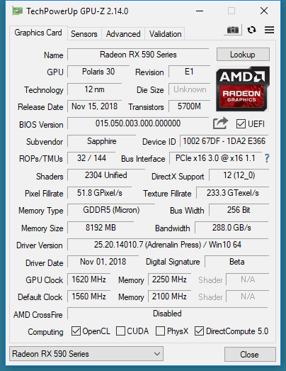 ” This design yields high performance, but the HD 5970 is quite expensive in addition to being big, heavy, and hot.
The GeForce GTX 580 is very much like the GTX 480. The 480 had one of the GF100’s 16 shader modules disabled, which effectively removed 32 of the shader units (nVidia calls them CUDA cores), four of the texture processing units, and one of the geometry processing engines. The new GF110 chip in the GTX 580 is nearly the same, but this time nVidia fully enables all of the chip’s functional units. Note the discrepancy in number of shader units between the AMD and nVidia cards in the chart above; this reflects the fact that the numbers are not directly comparable. Due to the different ways in which the nVidia and AMD chips are designed, a single shader unit in nVidia’s chip can do more work than one in AMD’s chip. It is also larger, which explains why there aren’t as many of them in the GPU.
Don’t miss our review of the nVidia GeForce GTX 580.
Next: GF100 Unleashed
GF100 Unleashed
At the chip level, the GeForce GTX 580 is essentially the same as the GTX 480. The new chip that powers it, called GF110, is made using TSMC’s 40-nanometer manufacturing process. It’s architecturally similar to the GF100, with the same dimensions and the same transistor count. If you were to look at a block diagram of the chip, it would look identical. Features such as cache sizes and the composition of the shader processors are the same. But with the GF110, nVidia fully retooled the chip from the transistor level, fixing many of the problems that make the GF100 hard to manufacture. This enabled the company to release a chip that has all the functional units enabled and yet draws less power and produces less heat than its predecessor. Together with better manufacturing and an enhanced cooling system, the GTX 580 runs the GF110 chip at a somewhat higher clock speed than the GF100 runs in the GTX 480.
There are no major new technologies in the GF110 GPU. It doesn’t have support for new display output types, for instance. Cards will have two dual-link DVI connectors, one mini-HDMI connector, and no DisplayPort. There is no new video decoder unit and no additional render back ends. That’s not to say that nVidia didn’t take the opportunity of remaking the chip to sneak in a few enhancements.
Cooler and quieter: Reworking the GF110 GPU has permitted nVidia to run it at a roughly 10 percent faster clock speed while drawing less wattage (about 20 watts less, in our tests). This is analogous to when a CPU company like Intel produces a new “stepping” of its CPU: The hardware is functionally identical, but it runs cooler. A new vapor-chamber heat spreader and a quieter fan design allow nVidia to cool the GeForce GTX 580 cards more efficiently and quietly, too.
Full-speed FP16 texture filtering: In the GF100, 16-bit floating point textures, often used in high-dynamic-range lighting, were filtered at half speed. Later chips in the Fermi line–for instance, the GF104 that powers the GeForce GTX 460–made some tweaks to filter these textures at full speed. The tweaks were rolled up into the GF110 GPU.
Faster z-culling: Modern graphics chips have a feature called z-culling. With z-culling in place, the graphics chip checks the depth of each part of an object in a scene to see whether something closer to the camera obscures it. If so, the chip rejects that part of the object so that it doesn’t have to do all the work necessary to draw it–you can’t see it anyway. This hardware is slightly improved in the GF110.
Power draw safeguard: The GF100 and nearly every nVidia card made to date will run as fast as possible when it’s in use; and the power draw, heat output, and cooling setups are all geared toward a worst-case scenario in which the GPU is being worked extremely hard. In rare conditions, a GPU may be asked to do too much, may get crazy hot, and may draw too much power from the PCIe power plugs. A perfect example of such conditions is the synthetic FurMark test, which made nVidia graphics cards run unusually hot and draw far more power than they were designed to. A few games have simple 3D rendered menu screens that do not impose an artificial cap on frame rate and can similarly cause too much heat and power draw. The GeForce GTX 580 has a new hardware feature that monitors power draw and will limit the GPU if necessary. This protective mechanism won’t affect performance in regular game situations, but it could affect performance on benchmarks like FurMark, and it should keep the card from getting loud and hot in those odd games that have misbehaving menus.
Next: Impressive Performance
Performance: Synthetic Benchmarks
nVidia promises that this $500 card, its new flagship, will be the fastest GPU that money can buy. That’s hedging a little bit: Technically, the Radeon HD 5970 is a single graphics card, but it uses two GPUs. Still, we think it’s worthwhile to compare the GeForce GTX 580 to the Radeon 5970, if only because the latter is the fastest single graphics card you can buy that uses AMD’s technology; it’s also a longer card that doesn’t easily fit into a midsize desktop PC case. In addition, we’ll compare the GeForce GTX 580 to the Radeon HD 5870 (the fastest single-GPU card that uses AMD’s tech) and to the GeForce GTX 480 (nVidia’s previous best card, which uses a very similar GPU).
We performed all of our benchmarks on a system configured with an Intel Core i7 980X CPU, and 6GB of RAM, and running 64-bit Windows 7.
Let’s start with the Unigine Heaven benchmark, a synthetic test of a real DirectX 11 game engine, currently licensed by a number of smaller games. The test is rather strenuous and forward-looking, featuring high detail levels, dynamic lighting and shadows, and lots of tessellation. We ran the test at the middle “Normal” mode. This geometry-heavy test favors nVidia’s architecture, and the new GTX 580 did great on the measure–around 20 percent faster than the GTX 480 and nearly 80 percent faster than the Radeon HD 5870.
FurMark is a synthetic OpenGL-based test that renders a torus covered in fur. It’s rather simple, but no test we’re aware of stresses a GPU more thoroughly.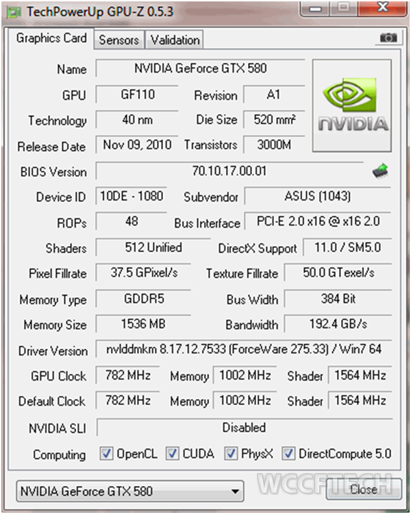 It’s a great way to see just how hot your graphics card will get, and how much power it will use. In the test results, you can see the effect of the new power draw safeguard kicking in. During this test, the GeForce GTX 480 got extremely loud and hot, and drew far more power than it was supposed to. It sounded like a leaf blower, though it also ran very fast. In contrast, the GTX 580 limited the power draw and scaled everything back to a reasonable level. If anything, the power restraint was too aggressive, as the AMD chips significantly outpaced the GTX 580. This test isn’t a very useful example of real-world performance, but it does nicely illustrate the power safeguard in action.
Though it’s getting a little long in the tooth, 3DMark Vantage is a standard still commonly used in synthetic graphics benchmarks. The engine utilizes DirectX 10 only, though a new version of 3DMark geared for DirectX 11 should be coming soon. We present the 3DMark score with standard settings for the “High” and “Extreme” profiles. AMD’s dual-GPU Radeon HD 5970 won this contest, but not by much.For its part, nVidia’s new card ran impressively fast, given that it is equipped with a single GPU. AMD’s best single-GPU card, the Radeon HD 5870, was left far behind.
Next: Real Game Performance
Performance: Games
Synthetic tests can be useful for evaluating features that will be common in tomorrow’s games, but performance in real games is far more important. We tested with five modern games that can push a modern graphics card to the limit.
Codemasters’ rally racer Dirt 2, one of the first DirectX 11 games, features an excellent built-in benchmark. We used the demo version (whose benchmark track differs from the track in the retail game), so you can run the game at home and compare your results. We enabled DirectX 11 and turned all of the detail levels up to full. The GeForce GTX 580 delivered very strong performance here, easily outpacing the Radeon HD 5970 (by 25 to 40 percent) and the Radeon HD 5870 (by as much as 80 percent). The new GTX 580 is about 20 percent faster than the GTX 480.
Tom Clancy’s H.A.W.X. is a graphically rich arcade flight game that uses DirectX 10.1 to enable features such as Screen Space Ambient Occlusion (SSAO), God Rays, and Soft Particles. Again, we turned all of the detail levels up to the maximum for our testing. Historically, AMD’s cards have performed extremely well on this test, and the dual-GPU Radeon HD 5970 outpaced the GeForce GTX 580 as well (though both cards achieved extremely high frame rates). The GTX 580 was about 20 percent faster than the GTX 480 on H.A.W.X., and roughly 30 to 50 percent faster than the Radeon HD 5870.
World in Conflict is aging a bit, but it’s still a beautiful real-time strategy game with a DirectX 10 based graphics engine that can stress all but the most powerful graphics cards when you maximize the detail levels, as we did. This is another game that AMD cards usually handle quite well. In our tests, the GTX 580 ran about 15 percent faster than its top-of-the-line nVidia predecessor, and 25 to 40 percent faster than the Radeon HD 5870. Only the dual-chip 5970 outpaced it.
The S.T.A.L.K.E.R. series has always been on the leading edge of graphics technology. We used the demo benchmark for the Call of Pripyat sequel with DirectX 11 lighting enabled and all detail settings maximized. The scores charted below represent the average of the four tests that the benchmark rans. With antialiasing applied, nVidia’s new card matched the Radeon HD 5970, and it dramatically outperformed the single-GPU Radeon HD 5870.
Last but not least, we used the excellent benchmark built in to Just Cause 2. We maximized graphics settings and ran the Concrete Jungle test, which is the most strenuous of benchmarks. Again the 5970 performed well, thanks to its essentially combining two Radeon HD 5870s on a single long card. The GTX 580 handily beat the solo 5870, especially when we turned on antialiasing. Interestingly, on this game only, the new GTX 580 was no faster than the GTX 480 with antialiasing off. This odd behavior is probably attributable to immature drivers.
Next: Value and Efficiency
Value and Efficiency
Our test lineup consists entirely of high-end graphics cards–products for performance-oriented enthusiasts who aren’t terribly concerned with finding the best bargain available. The GeForce GTX 580 is likely to sell for a suggested price of $500. nVidia tells us that the supply of GTX 580 cards will be small for the first few weeks, so prices may temporarily go a bit higher. The GeForce GTX 480 has dropped to $450, while AMD has adjusted the prices on its high-end cards a little: The Radeon HD 5870 starts at about $340 and the dual-GPU Radeon HD 5970 took a big price cut down to $500 to match nVidia’s latest and greatest.
Nobody wants to spend more than is necessary, and everyone wants to know which product delivers the most bang for the buck. To find out, we averaged the benchmark results for all of our real-world game tests and then divided by the price to arrive at a metric we call dollars per frames per second. On the chart below, lower numbers are better: They signify spending less to get equivalent performance.
Thanks to AMD’s recent price cuts, all four cards deliver fairly similar performance per dollar. Though the Radeon HD 5870 is significantly slower than the other three cards, it is also considerably less expensive. The only clear advantage appears at the very high resolution of 2650 by 1600 with no antialiasing, where AMD’s cards offer more oomph for the money.
nVidia says that it worked hard to optimize power utilization on the GeForce GTX 580, and it shows. Despite running at a higher clock speed, the GTX 580 delivered power reductions of about 20 watts both at idle and under full load. The lower-performing Radeon HD 5870 took the crown for power use here; but among the faster and more-expensive cards, the GTX 580 doesn’t look bad at all. Somewhat surprisingly, it uses more power under load than AMD’s dual-GPU card, but it uses less power at idle.
By dividing the average frames per second for each card on all of our game tests by its power use under load from the previous chart, we arrive at a measure of watts per frames per second. Instead of simply identifying how fast the cards were or how much power they used, this chart calculates their power efficiency. Here again, lower numbers are better.
As you can see, the purple bar is consistently much shorter than the green bar. This indicates how much progress nVidia has made with the GF110 GPU. Despite being the same size as the GF100 and having the same transistor count, the GF110 enabled the GeForce GTX 580 to deliver significantly better performance than the GTX 480 did, while lowering power consumption. It even turned in better performance per watt than the Radeon HD 5870.
Next: The Fastest Graphics Card Around…for Now
The Fastest GPU Around, but No New Features
The GeForce GTX 480 was supposed to be last year’s graphics champ, but it didn’t launch until March of this year. If the new GeForce GTX 580’s quick arrival on the market (only six months after its predecessor) is surprising, that is only because its the GTX 480 was so late.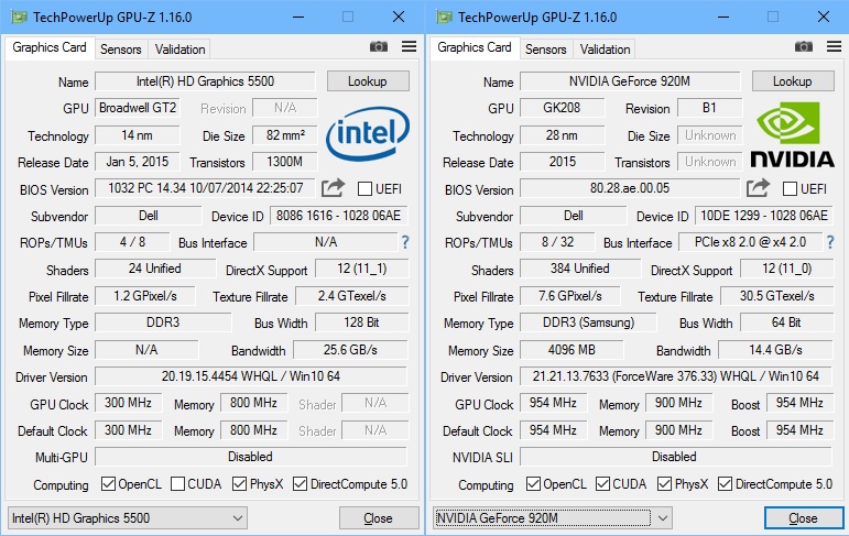 Under the circumstances, it’s hard not to be slightly disappointed by the GeForce GTX 580.
Its performance, mind you, is stellar. Thanks to a reworking of the GF100 GPU, nVidia can finally demonstrate what the architecture can accomplish when the chip is uncrippled and runs at a high clock speed. In our tests, the GTX 580 was roughly 20 to 30 percent faster than the GTX 480 (already quite a fast card) while drawing significantly less power; it’s quieter, too. We couldn’t be happier with its performance, and we can’t wait to see what AMD’s answer will be; the company’s high-end Radeon 6900 series is expected soon.
Our modest disappointment is that the GeForce GTX 580 is little more than a fixed GeForce GTX 480. It’s the graphics card that the GTX 480 should have been. nVidia is behind the curve on what we feel are important display options such as DisplayPort support, and the ability to drive three displays simultaneously from a single graphics card. New high-end products are the obvious place to introduce these types of features. With the exception of a couple tweaks to texture filtering and z-culling, however, the GPU didn’t receive any architectural enhancements at all.
In some ways, it just goes to show how hard it is to bring a 3-billion-transistor, over-500-square-millimeter graphics processor to market. nVidia took six months longer than it expected to get its new design out the door, and another six months to get it right. Now that it has, we have no reservations in recommending the GeForce GTX 580 as an enthusiast-class graphics card for price-be-damned gamers. True, the Radeon HD 5970 is slightly faster on average, but cards that rely on two GPUs carry their own set of drawbacks–for instance, extremely long board length, high idle power use, and the inability to perform as well as they should on games that run in windowed mode (multiple-GPU cards work best in full-screen mode).
Though it took the company a year longer than intended, nVidia has finally released a graphics card that can fully display the Fermi architecture’s capabilities, and they’re impressive. Whatever qualms we may have about its lack of DisplayPort or its inability to drive more than two displays with a single card, the GeForce GTX 580 certainly makes good on nVidia’s promise to deliver the fastest single-GPU graphics card.
Be sure to read our review of the GeForce GTX 580.
GTX 580 benchmark with Ryzen 5 3600 1080p, 1440p, Ultrawide, 4K benchmarks at Ultra Quality
Compare To
Select..AMD Radeon 530 Mobile — $ 636AMD Radeon 540 Mobile — $ 1,086AMD Radeon HD 6850 — $ 199AMD Radeon HD 6870 — $ 199AMD Radeon HD 6950 — $ 250AMD Radeon HD 6970 — $ 299AMD Radeon HD 6990 — $ 699AMD Radeon HD 7750 — $ 140AMD Radeon HD 7750M — $ 858AMD Radeon HD 7790 — $ 149AMD Radeon HD 7850 — $ 249AMD Radeon HD 7850M — $ 964AMD Radeon HD 7950 — $ 149AMD Radeon HD 7950M — $ 1,023AMD Radeon HD 7970 — $ 299AMD Radeon HD 7970 GHz Edition — $ 299AMD Radeon HD 7970M — $ 1,079AMD Radeon HD 7990 — $ 999AMD Radeon Pro WX 7100 Mobile — $ 1,959AMD Radeon R5 — $ 710AMD Radeon R5 — $ 701AMD Radeon R7 250 — $ 95AMD Radeon R7 265 — $ 149AMD Radeon R7 370 — $ 202AMD Radeon R9 270 — $ 275AMD Radeon R9 280 — $ 350AMD Radeon R9 280X — $ 350AMD Radeon R9 285 — $ 380AMD Radeon R9 290 — $ 310AMD Radeon R9 290X — $ 399AMD Radeon R9 295X2 — $ 1,499AMD Radeon R9 380 — $ 299AMD Radeon R9 380X — $ 229AMD Radeon R9 390 — $ 465AMD Radeon R9 390X — $ 495AMD Radeon R9 FURY — $ 549AMD Radeon R9 FURY X — $ 649AMD Radeon R9 M270X — $ 1,016AMD Radeon R9 M280X — $ 1,070AMD Radeon R9 M280X 2GB — $ 1,070AMD Radeon R9 M290X — $ 1,209AMD Radeon R9 M380 — $ 1,074AMD Radeon R9 Nano — $ 1,529AMD Radeon RX 460 — $ 140AMD Radeon RX 470 — $ 342AMD Radeon RX 470 Mobile — $ 1,203AMD Radeon RX 480 — $ 399AMD Radeon RX 480 Mobile — $ 1,275AMD Radeon RX 540 Mobile — $ 645AMD Radeon RX 550 — $ 74AMD Radeon RX 550 Mobile — $ 923AMD Radeon RX 5500 XT 4GB — $ 169AMD Radeon RX 5500 XT 8GB — $ 199AMD Radeon RX 550X Mobile — $ 923AMD Radeon RX 560 — $ 99AMD Radeon RX 560 Mobile — $ 987AMD Radeon RX 5600 XT — $ 279AMD Radeon RX 560X Mobile — $ 641AMD Radeon RX 560X Mobile 2GB — $ 987AMD Radeon RX 570 — $ 123AMD Radeon RX 570 Mobile — $ 1,260AMD Radeon RX 5700 — $ 349AMD Radeon RX 5700 XT — $ 399AMD Radeon RX 580 — $ 151AMD Radeon RX 580 Mobile — $ 1,307AMD Radeon RX 580X Mobile — $ 1,307AMD Radeon RX 590 — $ 214AMD Radeon RX 6600 XT — $ 379AMD Radeon RX 6700 XT — $ 479AMD Radeon RX 6800 — $ 579AMD Radeon RX 6800 XT — $ 649AMD Radeon RX 6900 XT — $ 999AMD Radeon RX VEGA 10 — $ 632AMD Radeon RX VEGA 3 — $ 567AMD Radeon RX VEGA 6 — $ 1,119AMD Radeon RX VEGA 8 — $ 601AMD Radeon RX Vega 56 — $ 269AMD Radeon RX Vega 56 Mobile — $ 1,579AMD Radeon RX Vega 64 — $ 419AMD Radeon VII — $ 664ATI Radeon HD 4870 — $ 299NVIDIA GeForce GT 1030 — $ 79NVIDIA GeForce GT 640 — $ 79NVIDIA GeForce GTS 450 — $ 199NVIDIA GeForce GTX 1050 — $ 129NVIDIA GeForce GTX 1050 Max-Q — $ 1,282NVIDIA GeForce GTX 1050 Mobile — $ 750NVIDIA GeForce GTX 1050 Mobile 2GB — $ 1,062NVIDIA GeForce GTX 1050 Ti — $ 129NVIDIA GeForce GTX 1050 Ti Max-Q — $ 1,270NVIDIA GeForce GTX 1050 Ti Mobile — $ 876NVIDIA GeForce GTX 1060 3GB — $ 170NVIDIA GeForce GTX 1060 6GB — $ 159NVIDIA GeForce GTX 1060 Max-Q — $ 1,185NVIDIA GeForce GTX 1060 Mobile — $ 987NVIDIA GeForce GTX 1070 — $ 329NVIDIA GeForce GTX 1070 Max-Q — $ 1,106NVIDIA GeForce GTX 1070 Mobile — $ 1,559NVIDIA GeForce GTX 1070 Ti — $ 503NVIDIA GeForce GTX 1080 — $ 522NVIDIA GeForce GTX 1080 Max-Q — $ 1,955NVIDIA GeForce GTX 1080 Mobile — $ 1,857NVIDIA GeForce GTX 1080 Ti — $ 807NVIDIA GeForce GTX 1650 — $ 149NVIDIA GeForce GTX 1650 Max-Q — $ 1,239NVIDIA GeForce GTX 1650 Mobile — $ 1,151NVIDIA GeForce GTX 1650 SUPER — $ 160NVIDIA GeForce GTX 1660 — $ 220NVIDIA GeForce GTX 1660 SUPER — $ 229NVIDIA GeForce GTX 1660 Ti — $ 279NVIDIA GeForce GTX 1660 Ti Max-Q — $ 1,185NVIDIA GeForce GTX 1660 Ti Mobile — $ 1,758NVIDIA GeForce GTX 260 — $ 449NVIDIA GeForce GTX 260 Core 216 — $ 299NVIDIA GeForce GTX 280 — $ 649NVIDIA GeForce GTX 285 — $ 249NVIDIA GeForce GTX 470 — $ 299NVIDIA GeForce GTX 480 — $ 499NVIDIA GeForce GTX 550 Ti — $ 199NVIDIA GeForce GTX 560 — $ 153NVIDIA GeForce GTX 560 Ti — $ 220NVIDIA GeForce GTX 570 — $ 349NVIDIA GeForce GTX 590 — $ 699NVIDIA GeForce GTX 650 — $ 49NVIDIA GeForce GTX 650 Ti — $ 64NVIDIA GeForce GTX 650 Ti Boost — $ 169NVIDIA GeForce GTX 660 — $ 79NVIDIA GeForce GTX 660 Ti — $ 299NVIDIA GeForce GTX 660M — $ 987NVIDIA GeForce GTX 670 — $ 79NVIDIA GeForce GTX 670M — $ 1,058NVIDIA GeForce GTX 670MX — $ 1,058NVIDIA GeForce GTX 680 — $ 485NVIDIA GeForce GTX 680M — $ 1,083NVIDIA GeForce GTX 690 — $ 439NVIDIA GeForce GTX 750 Ti — $ 279NVIDIA GeForce GTX 760 — $ 320NVIDIA GeForce GTX 760M — $ 1,036NVIDIA GeForce GTX 770 — $ 179NVIDIA GeForce GTX 770M — $ 1,100NVIDIA GeForce GTX 780 — $ 355NVIDIA GeForce GTX 780 Ti — $ 410NVIDIA GeForce GTX 780M — $ 1,162NVIDIA GeForce GTX 780M — $ 1,162NVIDIA GeForce GTX 950 — $ 89NVIDIA GeForce GTX 960 — $ 89NVIDIA GeForce GTX 960M — $ 1,066NVIDIA GeForce GTX 970 — $ 449NVIDIA GeForce GTX 970M — $ 1,249NVIDIA GeForce GTX 970M 6GB — $ 1,249NVIDIA GeForce GTX 980 — $ 249NVIDIA GeForce GTX 980 Mobile — $ 1,345NVIDIA GeForce GTX 980 Ti — $ 619NVIDIA GeForce GTX 980M — $ 1,345NVIDIA GeForce GTX 980MX — $ 1,345NVIDIA GeForce GTX TITAN — $ 650NVIDIA GeForce GTX TITAN BLACK — $ 999NVIDIA GeForce GTX TITAN X — $ 1,099NVIDIA GeForce RTX 2060 — $ 349NVIDIA GeForce RTX 2060 Mobile — $ 1,104NVIDIA GeForce RTX 2060 SUPER — $ 400NVIDIA GeForce RTX 2070 — $ 469NVIDIA GeForce RTX 2070 Max-Q — $ 1,516NVIDIA GeForce RTX 2070 Mobile — $ 1,724NVIDIA GeForce RTX 2070 SUPER — $ 499NVIDIA GeForce RTX 2080 — $ 693NVIDIA GeForce RTX 2080 Max-Q — $ 1,772NVIDIA GeForce RTX 2080 Mobile — $ 1,942NVIDIA GeForce RTX 2080 SUPER — $ 699NVIDIA GeForce RTX 2080 Ti — $ 1,187NVIDIA GeForce RTX 3050 — $ 200NVIDIA GeForce RTX 3050 Ti — $ 249NVIDIA GeForce RTX 3060 — $ 329NVIDIA GeForce RTX 3060 Ti — $ 399NVIDIA GeForce RTX 3070 — $ 499NVIDIA GeForce RTX 3070 Ti — $ 599NVIDIA GeForce RTX 3080 — $ 699NVIDIA GeForce RTX 3080 Ti — $ 799NVIDIA GeForce RTX 3090 — $ 1,499NVIDIA GeForce RTX 4050 — $ 200NVIDIA GeForce RTX 4060 — $ 329NVIDIA GeForce RTX 4060 Ti — $ 399NVIDIA GeForce RTX 4070 — $ 499NVIDIA GeForce RTX 4080 — $ 699NVIDIA GeForce RTX 4080 Ti — $ 799NVIDIA GeForce RTX 4090 — $ 1,499NVIDIA TITAN RTX — $ 2,499NVIDIA TITAN V — $ 2,999NVIDIA TITAN Xp — $ 1,199
Change CPU To
Select. .AMD Athlon 5000 Dual-Core — $ 100AMD Athlon 5200 Dual-Core — $ 30AMD Athlon 64 X2 Dual Core 4200+ — $ 130AMD Athlon 64 X2 Dual Core 4400+ — $ 60AMD Athlon 64 X2 Dual Core 4600+ — $ 360AMD Athlon 64 X2 Dual Core 4800+ — $ 460AMD Athlon 64 X2 Dual Core 5000+ — $ 331.5AMD Athlon 64 X2 Dual Core 5200+ — $ 53.1AMD Athlon 64 X2 Dual Core 5400+ — $ 53AMD Athlon 64 X2 Dual Core 5600+ — $ 150AMD Athlon 64 X2 Dual Core 5800+ — $ 25AMD Athlon 64 X2 Dual Core 6000+ — $ 46AMD Athlon 64 X2 Dual Core 6400+ — $ 260AMD Athlon 7550 Dual-Core — $ 60AMD Athlon 7750 Dual-Core — $ 148.7AMD Athlon 7850 Dual-Core — $ 209.7AMD Athlon Dual Core 5000B — $ 95AMD Athlon II X2 215 — $ 12AMD Athlon II X2 220 — $ 32.2AMD Athlon II X2 240 — $ 35AMD Athlon II X2 245 — $ 35AMD Athlon II X2 250 — $ 39AMD Athlon II X2 255 — $ 65.2AMD Athlon II X2 260 — $ 20AMD Athlon II X2 265 — $ 82.9AMD Athlon II X2 270 — $ 24AMD Athlon II X2 B22 — $ 36AMD Athlon II X2 B24 — $ 40AMD Athlon II X2 B28 — $ 49.1AMD Athlon II X3 425 — $ 104.
 2AMD Athlon II X3 435 — $ 50AMD Athlon II X3 440 — $ 47AMD Athlon II X3 445 — $ 91AMD Athlon II X3 450 — $ 40AMD Athlon II X3 455 — $ 116.9AMD Athlon II X3 460 — $ 50AMD Athlon II X4 620 — $ 60AMD Athlon II X4 630 — $ 43AMD Athlon II X4 631 Quad-Core — $ 80AMD Athlon II X4 635 — $ 70AMD Athlon II X4 640 — $ 80AMD Athlon II X4 641 Quad-Core — $ 91.5AMD Athlon II X4 645 — $ 50AMD Athlon X4 740 Quad Core — $ 277AMD Athlon X4 760K Quad Core — $ 46AMD Athlon X4 840 — $ 78.7AMD Athlon X4 845 — $ 50AMD Athlon X4 860K — $ 64AMD Athlon X4 870K — $ 80AMD Athlon X4 880K — $ 90AMD Athlon X4 950 — $ 60AMD E2-3200 APU — $ 8AMD FX-4100 Quad-Core — $ 130AMD FX-4130 Quad-Core — $ 76AMD FX-4170 Quad-Core — $ 100AMD FX-4200 Quad-Core — $ 228.2AMD FX-4300 Quad-Core — $ 53.4AMD FX-4350 Quad-Core — $ 130AMD FX-6200 Six-Core — $ 340AMD FX-6300 Six-Core — $ 59AMD FX-6350 Six-Core — $ 130AMD FX-8120 Eight-Core — $ 100AMD FX-8150 Eight-Core — $ 383.5AMD FX-8300 Eight-Core — $ 80.6AMD FX-8320 Eight-Core — $ 79.5AMD FX-8320E Eight-Core — $ 98.
 9AMD FX-8350 Eight-Core — $ 80AMD FX-8370 Eight-Core — $ 135AMD FX-8370E Eight-Core — $ 180AMD FX-9370 Eight-Core — $ 178.9AMD FX-9590 Eight-Core — $ 122AMD Phenom 8250e Triple-Core — $ 47AMD Phenom 8450 Triple-Core — $ 30AMD Phenom 8600 Triple-Core — $ 53AMD Phenom 8600B Triple-Core — $ 53AMD Phenom 8650 Triple-Core — $ 50AMD Phenom 9100e Quad-Core — $ 40AMD Phenom 9150e Quad-Core — $ 40AMD Phenom 9350e Quad-Core — $ 3382.1AMD Phenom 9450e Quad-Core — $ 105AMD Phenom 9500 Quad-Core — $ 60AMD Phenom 9550 Quad-Core — $ 40AMD Phenom 9600 Quad-Core — $ 50AMD Phenom 9600B Quad-Core — $ 147.2AMD Phenom 9650 Quad-Core — $ 55AMD Phenom 9750 Quad-Core — $ 60AMD Phenom 9850 Quad-Core — $ 50AMD Phenom 9950 Quad-Core — $ 180AMD Phenom II X2 545 — $ 44AMD Phenom II X2 550 — $ 50AMD Phenom II X2 555 — $ 142.1AMD Phenom II X2 565 — $ 30AMD Phenom II X2 B55 — $ 48AMD Phenom II X3 705e — $ 152.3AMD Phenom II X3 710 — $ 84.5AMD Phenom II X3 720 — $ 70AMD Phenom II X3 B73 — $ 75AMD Phenom II X4 805 — $ 174AMD Phenom II X4 810 — $ 116AMD Phenom II X4 820 — $ 75AMD Phenom II X4 840 — $ 90AMD Phenom II X4 905e — $ 212.
 4AMD Phenom II X4 910 — $ 100AMD Phenom II X4 910e — $ 157AMD Phenom II X4 920 — $ 67AMD Phenom II X4 925 — $ 160AMD Phenom II X4 940 — $ 120AMD Phenom II X4 945 — $ 50AMD Phenom II X4 955 — $ 130.2AMD Phenom II X4 960T — $ 135AMD Phenom II X4 965 — $ 59.5AMD Phenom II X4 B95 — $ 73AMD Phenom II X4 B97 — $ 90AMD Phenom II X6 1035T — $ 189AMD Phenom II X6 1045T — $ 175AMD Phenom II X6 1055T — $ 185AMD Phenom II X6 1075T — $ 260AMD Phenom II X6 1090T — $ 396.1AMD Phenom II X6 1100T — $ 200AMD Phenom X3 8550 — $ 170AMD Ryzen 3 1200 — $ 95AMD Ryzen 3 1300X — $ 125AMD Ryzen 3 2200G — $ 98AMD Ryzen 3 3100 — $ 90AMD Ryzen 3 3200G — $ 99AMD Ryzen 3 3300X — $ 120AMD Ryzen 5 1400 — $ 134AMD Ryzen 5 1500X — $ 144.9AMD Ryzen 5 1600 — $ 155AMD Ryzen 5 1600X — $ 178.4AMD Ryzen 5 2400G — $ 159AMD Ryzen 5 2600 — $ 150AMD Ryzen 5 2600X — $ 210AMD Ryzen 5 3400G — $ 150AMD Ryzen 5 3500 — $ 148AMD Ryzen 5 3500X — $ 160.5AMD Ryzen 5 3600 — $ 199AMD Ryzen 5 3600X — $ 249AMD Ryzen 5 5500 — $ 160AMD Ryzen 5 5600X — $ 299AMD Ryzen 7 1700 — $ 190AMD Ryzen 7 1700X — $ 200AMD Ryzen 7 1800X — $ 250AMD Ryzen 7 2700 — $ 249.
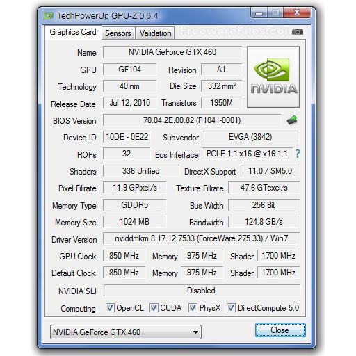 2AMD Ryzen 7 2700X — $ 305AMD Ryzen 7 3700X — $ 330AMD Ryzen 7 3800X — $ 399AMD Ryzen 7 5700X — $ 300AMD Ryzen 7 5800X — $ 399AMD Ryzen 7 5800X3D — $ 450AMD Ryzen 9 3900X — $ 499AMD Ryzen 9 3950X — $ 750AMD Ryzen 9 5900X — $ 499AMD Ryzen 9 5950X — $ 710AMD Ryzen Threadripper 1900X — $ 350AMD Ryzen Threadripper 1920X — $ 420AMD Ryzen Threadripper 1950X — $ 680AMD Ryzen Threadripper 2950X — $ 900AMD Ryzen Threadripper 2990WX — $ 1720Intel Core i3-10100 — $ 122Intel Core i3-10300 — $ 143Intel Core i3-11100 — $ 122Intel Core i3-11300 — $ 143Intel Core i3-12100 — $ 122Intel Core i3-12300 — $ 143Intel Core i3-2100 @ 3.10GHz — $ 60Intel Core i3-2102 @ 3.10GHz — $ 58Intel Core i3-2105 @ 3.10GHz — $ 80Intel Core i3-2120 @ 3.30GHz — $ 30Intel Core i3-2125 @ 3.30GHz — $ 199Intel Core i3-2130 @ 3.40GHz — $ 70Intel Core i3-3210 @ 3.20GHz — $ 100Intel Core i3-3220 @ 3.30GHz — $ 34.9Intel Core i3-3225 @ 3.30GHz — $ 100Intel Core i3-3240 @ 3.40GHz — $ 46Intel Core i3-3245 @ 3.40GHz — $ 80Intel Core i3-3250 @ 3.
 50GHz — $ 95Intel Core i3-4130 @ 3.40GHz — $ 140Intel Core i3-4150 @ 3.50GHz — $ 260Intel Core i3-4160 @ 3.60GHz — $ 140Intel Core i3-4170 @ 3.70GHz — $ 150Intel Core i3-4330 @ 3.50GHz — $ 180Intel Core i3-4340 @ 3.60GHz — $ 170Intel Core i3-4350 @ 3.60GHz — $ 170Intel Core i3-4360 @ 3.70GHz — $ 280Intel Core i3-4370 @ 3.80GHz — $ 450Intel Core i3-530 @ 2.93GHz — $ 20Intel Core i3-540 @ 3.07GHz — $ 21Intel Core i3-550 @ 3.20GHz — $ 180Intel Core i3-560 @ 3.33GHz — $ 30Intel Core i3-6098P @ 3.60GHz — $ 133.7Intel Core i3-6100 @ 3.70GHz — $ 166.1Intel Core i3-6300 @ 3.80GHz — $ 143Intel Core i3-6320 @ 3.90GHz — $ 160Intel Core i3-7100 @ 3.90GHz — $ 170Intel Core i3-7300 @ 4.00GHz — $ 210Intel Core i3-7320 @ 4.10GHz — $ 174.8Intel Core i3-7350K @ 4.20GHz — $ 230Intel Core i3-8100 @ 3.60GHz — $ 130Intel Core i3-8300 @ 3.70GHz — $ 179.4Intel Core i3-8350K @ 4.00GHz — $ 184Intel Core i3-9100 @ 3.60GHz — $ 170Intel Core i3-9100F @ 3.60GHz — $ 105Intel Core i3-9320 @ 3.70GHz — $ 162Intel Core i3-9350KF @ 4.
 00GHz — $ 224Intel Core i5 750S @ 2.40GHz — $ 100Intel Core i5-10400 — $ 182Intel Core i5-10600K — $ 236.8Intel Core i5-11400 — $ 182Intel Core i5-11600K — $ 262Intel Core i5-12400 — $ 143Intel Core i5-12600K — $ 290Intel Core i5-2300 @ 2.80GHz — $ 80Intel Core i5-2310 @ 2.90GHz — $ 80Intel Core i5-2320 @ 3.00GHz — $ 195.3Intel Core i5-2380P @ 3.10GHz — $ 90Intel Core i5-2400 @ 3.10GHz — $ 84Intel Core i5-2400S @ 2.50GHz — $ 65.7Intel Core i5-2405S @ 2.50GHz — $ 164.4Intel Core i5-2450P @ 3.20GHz — $ 90Intel Core i5-2500 @ 3.30GHz — $ 105Intel Core i5-2500K @ 3.30GHz — $ 124Intel Core i5-2500S @ 2.70GHz — $ 75Intel Core i5-2550K @ 3.40GHz — $ 130Intel Core i5-3330 @ 3.00GHz — $ 100Intel Core i5-3330S @ 2.70GHz — $ 95Intel Core i5-3340 @ 3.10GHz — $ 262Intel Core i5-3340S @ 2.80GHz — $ 150Intel Core i5-3350P @ 3.10GHz — $ 170Intel Core i5-3450 @ 3.10GHz — $ 128Intel Core i5-3450S @ 2.80GHz — $ 100Intel Core i5-3470 @ 3.20GHz — $ 125Intel Core i5-3470S @ 2.90GHz — $ 140.1Intel Core i5-3475S @ 2.
 90GHz — $ 143.5Intel Core i5-3550 @ 3.30GHz — $ 330Intel Core i5-3550S @ 3.00GHz — $ 341Intel Core i5-3570 @ 3.40GHz — $ 140Intel Core i5-3570K @ 3.40GHz — $ 144Intel Core i5-3570S @ 3.10GHz — $ 285Intel Core i5-4430 @ 3.00GHz — $ 180Intel Core i5-4430S @ 2.70GHz — $ 160Intel Core i5-4440 @ 3.10GHz — $ 170Intel Core i5-4440S @ 2.80GHz — $ 463Intel Core i5-4460 @ 3.20GHz — $ 170Intel Core i5-4460S @ 2.90GHz — $ 660Intel Core i5-4570 @ 3.20GHz — $ 175Intel Core i5-4570S @ 2.90GHz — $ 221.6Intel Core i5-4590 @ 3.30GHz — $ 185Intel Core i5-4590S @ 3.00GHz — $ 198Intel Core i5-4670 @ 3.40GHz — $ 188Intel Core i5-4670K @ 3.40GHz — $ 250Intel Core i5-4670R @ 3.00GHz — $ 276Intel Core i5-4690 @ 3.50GHz — $ 200Intel Core i5-4690K @ 3.50GHz — $ 200Intel Core i5-4690S @ 3.20GHz — $ 269.9Intel Core i5-5675C @ 3.10GHz — $ 400Intel Core i5-6400 @ 2.70GHz — $ 200Intel Core i5-6402P @ 2.80GHz — $ 190Intel Core i5-650 @ 3.20GHz — $ 100Intel Core i5-6500 @ 3.20GHz — $ 234.4Intel Core i5-655K @ 3.20GHz — $ 60Intel Core i5-660 @ 3.
 33GHz — $ 49Intel Core i5-6600 @ 3.30GHz — $ 220Intel Core i5-6600K @ 3.50GHz — $ 288.9Intel Core i5-661 @ 3.33GHz — $ 100Intel Core i5-670 @ 3.47GHz — $ 90Intel Core i5-680 @ 3.60GHz — $ 90Intel Core i5-7400 @ 3.00GHz — $ 213.5Intel Core i5-750 @ 2.67GHz — $ 160.5Intel Core i5-7500 @ 3.40GHz — $ 210Intel Core i5-760 @ 2.80GHz — $ 100Intel Core i5-7600 @ 3.50GHz — $ 240Intel Core i5-7600K @ 3.80GHz — $ 251Intel Core i5-7640X @ 4.00GHz — $ 250Intel Core i5-8400 @ 2.80GHz — $ 200Intel Core i5-8500 @ 3.00GHz — $ 239Intel Core i5-8600 @ 3.10GHz — $ 244.5Intel Core i5-8600K @ 3.60GHz — $ 377.7Intel Core i5-9400 @ 2.90GHz — $ 170Intel Core i5-9400F @ 2.90GHz — $ 170Intel Core i5-9600K @ 3.70GHz — $ 280Intel Core i5-9600KF @ 3.70GHz — $ 215Intel Core i7-10700K — $ 409.1Intel Core i7-11700K — $ 410Intel Core i7-12700K — $ 470Intel Core i7-2600 @ 3.40GHz — $ 150Intel Core i7-2600K @ 3.40GHz — $ 198Intel Core i7-2600S @ 2.80GHz — $ 200Intel Core i7-2700K @ 3.50GHz — $ 200Intel Core i7-3770 @ 3.40GHz — $ 179Intel Core i7-3770K @ 3.
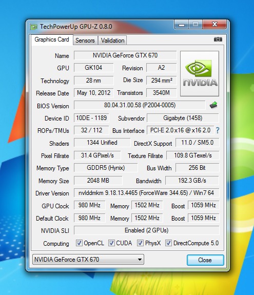 50GHz — $ 249Intel Core i7-3770S @ 3.10GHz — $ 200Intel Core i7-3820 @ 3.60GHz — $ 200Intel Core i7-3930K @ 3.20GHz — $ 399Intel Core i7-3960X @ 3.30GHz — $ 800Intel Core i7-3970X @ 3.50GHz — $ 954Intel Core i7-4770 @ 3.40GHz — $ 240Intel Core i7-4770K @ 3.50GHz — $ 285Intel Core i7-4770S @ 3.10GHz — $ 250Intel Core i7-4771 @ 3.50GHz — $ 300Intel Core i7-4790 @ 3.60GHz — $ 279Intel Core i7-4790K @ 4.00GHz — $ 307Intel Core i7-4790S @ 3.20GHz — $ 342.6Intel Core i7-4820K @ 3.70GHz — $ 500Intel Core i7-4930K @ 3.40GHz — $ 399Intel Core i7-4960X @ 3.60GHz — $ 770Intel Core i7-5775C @ 3.30GHz — $ 450Intel Core i7-5820K @ 3.30GHz — $ 300Intel Core i7-5930K @ 3.50GHz — $ 499Intel Core i7-5960X @ 3.00GHz — $ 770Intel Core i7-6700 @ 3.40GHz — $ 433.7Intel Core i7-6700K @ 4.00GHz — $ 335Intel Core i7-6800K @ 3.40GHz — $ 420Intel Core i7-6850K @ 3.60GHz — $ 550Intel Core i7-6900K @ 3.20GHz — $ 1200Intel Core i7-6950X @ 3.00GHz — $ 1576Intel Core i7-7700 @ 3.60GHz — $ 325.1Intel Core i7-7700K @ 4.
 20GHz — $ 355Intel Core i7-7740X @ 4.30GHz — $ 349Intel Core i7-7800X @ 3.50GHz — $ 370Intel Core i7-7820X @ 3.60GHz — $ 930Intel Core i7-8086K @ 4.00GHz — $ 553Intel Core i7-860 @ 2.80GHz — $ 290Intel Core i7-860S @ 2.53GHz — $ 200Intel Core i7-870 @ 2.93GHz — $ 310Intel Core i7-8700 @ 3.20GHz — $ 454.5Intel Core i7-8700K @ 3.70GHz — $ 369.9Intel Core i7-875K @ 2.93GHz — $ 200Intel Core i7-880 @ 3.07GHz — $ 583Intel Core i7-920 @ 2.67GHz — $ 174Intel Core i7-930 @ 2.80GHz — $ 60Intel Core i7-940 @ 2.93GHz — $ 70.7Intel Core i7-950 @ 3.07GHz — $ 245Intel Core i7-960 @ 3.20GHz — $ 100Intel Core i7-965 @ 3.20GHz — $ 140Intel Core i7-970 @ 3.20GHz — $ 150Intel Core i7-9700 @ 3.00GHz — $ 330Intel Core i7-9700F @ 3.00GHz — $ 368Intel Core i7-9700K @ 3.60GHz — $ 410Intel Core i7-975 @ 3.33GHz — $ 180Intel Core i7-980 @ 3.33GHz — $ 200Intel Core i7-980X @ 3.33GHz — $ 220Intel Core i7-990X @ 3.47GHz — $ 350Intel Core i9-10900K — $ 590Intel Core i9-11900K — $ 488Intel Core i9-12900K — $ 590Intel Core i9-7900X @ 3.
 30GHz — $ 1380Intel Core i9-7920X @ 2.90GHz — $ 1096.7Intel Core i9-7940X @ 3.10GHz — $ 1192.1Intel Core i9-7960X @ 2.80GHz — $ 2000Intel Core i9-7980XE @ 2.60GHz — $ 2005.5Intel Core i9-9900 @ 3.10GHz — $ 440Intel Core i9-9900K @ 3.60GHz — $ 835Intel Core2 Duo E4300 @ 1.80GHz — $ 158Intel Core2 Duo E4400 @ 2.00GHz — $ 9Intel Core2 Duo E4500 @ 2.20GHz — $ 40Intel Core2 Duo E4600 @ 2.40GHz — $ 158Intel Core2 Duo E4700 @ 2.60GHz — $ 100Intel Core2 Duo E6300 @ 1.86GHz — $ 13Intel Core2 Duo E6320 @ 1.86GHz — $ 50Intel Core2 Duo E6400 @ 2.13GHz — $ 20Intel Core2 Duo E6420 @ 2.13GHz — $ 50Intel Core2 Duo E6550 @ 2.33GHz — $ 15Intel Core2 Duo E6600 @ 2.40GHz — $ 15Intel Core2 Duo E6700 @ 2.66GHz — $ 30Intel Core2 Duo E6750 @ 2.66GHz — $ 13Intel Core2 Duo E6850 @ 3.00GHz — $ 50Intel Core2 Duo E7200 @ 2.53GHz — $ 75Intel Core2 Duo E7300 @ 2.66GHz — $ 20Intel Core2 Duo E7400 @ 2.80GHz — $ 29Intel Core2 Duo E7500 @ 2.93GHz — $ 15Intel Core2 Duo E7600 @ 3.06GHz — $ 120Intel Core2 Duo E8200 @ 2.66GHz — $ 50Intel Core2 Duo E8300 @ 2.
 83GHz — $ 20Intel Core2 Duo E8400 @ 3.00GHz — $ 9.8Intel Core2 Duo E8500 @ 3.16GHz — $ 40Intel Core2 Duo E8600 @ 3.33GHz — $ 50Intel Core2 Extreme Q6800 @ 2.93GHz — $ 1125Intel Core2 Extreme Q6850 @ 3.00GHz — $ 1496Intel Core2 Extreme X6800 @ 2.93GHz — $ 263.6Intel Core2 Extreme X9650 @ 3.00GHz — $ 909Intel Core2 Extreme X9770 @ 3.20GHz — $ 1609Intel Core2 Extreme X9775 @ 3.20GHz — $ 1806Intel Core2 Quad Q6600 @ 2.40GHz — $ 40Intel Core2 Quad Q6700 @ 2.66GHz — $ 45Intel Core2 Quad Q8200 @ 2.33GHz — $ 23Intel Core2 Quad Q8300 @ 2.50GHz — $ 50Intel Core2 Quad Q8400 @ 2.66GHz — $ 99.5Intel Core2 Quad Q9300 @ 2.50GHz — $ 50Intel Core2 Quad Q9400 @ 2.66GHz — $ 34Intel Core2 Quad Q9450 @ 2.66GHz — $ 335Intel Core2 Quad Q9500 @ 2.83GHz — $ 35Intel Core2 Quad Q9505 @ 2.83GHz — $ 190Intel Core2 Quad Q9550 @ 2.83GHz — $ 49Intel Core2 Quad Q9650 @ 3.00GHz — $ 69.8Intel Pentium G2010 @ 2.80GHz — $ 34.9Intel Pentium G2020 @ 2.90GHz — $ 32.9Intel Pentium G2030 @ 3.00GHz — $ 41Intel Pentium G2120 @ 3.
 10GHz — $ 46Intel Pentium G2130 @ 3.20GHz — $ 50Intel Pentium G2140 @ 3.30GHz — $ 50Intel Pentium G3220 @ 3.00GHz — $ 120Intel Pentium G3240 @ 3.10GHz — $ 80Intel Pentium G3250 @ 3.20GHz — $ 110Intel Pentium G3258 @ 3.20GHz — $ 178.3Intel Pentium G3260 @ 3.30GHz — $ 105Intel Pentium G3420 @ 3.20GHz — $ 110Intel Pentium G3430 @ 3.30GHz — $ 90Intel Pentium G3440 @ 3.30GHz — $ 159.9Intel Pentium G3450 @ 3.40GHz — $ 100Intel Pentium G3460 @ 3.50GHz — $ 288.2Intel Pentium G3470 @ 3.60GHz — $ 104.3Intel Pentium G4400 @ 3.30GHz — $ 80Intel Pentium G4500 @ 3.50GHz — $ 85.3Intel Pentium G4520 @ 3.60GHz — $ 110.9Intel Pentium G4560 @ 3.50GHz — $ 103.1Intel Pentium G4600 @ 3.60GHz — $ 100Intel Pentium G4620 @ 3.70GHz — $ 105.9Intel Pentium G640 @ 2.80GHz — $ 25Intel Pentium G645 @ 2.90GHz — $ 95Intel Pentium G840 @ 2.80GHz — $ 35Intel Pentium G850 @ 2.90GHz — $ 30Intel Pentium G860 @ 3.00GHz — $ 30Intel Pentium G870 @ 3.10GHz — $ 97Intel Pentium Gold G5400 @ 3.70GHz — $ 123.9Intel Pentium Gold G5500 @ 3.
 80GHz — $ 100.3Intel Pentium Gold G5600 @ 3.90GHz — $ 100.9
Change Variant To
Select..ASUS GTX 580 DirectCU IIASUS ROG Matrix GTX 580ASUS ROG Matrix GTX 580 PlatinumClub 3D GTX 580Colorful GTX 580 OCEVGA GTX 580EVGA GTX 580 3 GBEVGA GTX 580 Batman: Arkham CityEVGA GTX 580 Black OpsEVGA GTX 580 CLASSIFIEDEVGA GTX 580 CLASSIFIED 3 GBEVGA GTX 580 CLASSIFIED Hydro CopperEVGA GTX 580 CLASSIFIED UltraEVGA GTX 580 CLASSIFIED Ultra Hydro CopperEVGA GTX 580 DS SuperclockedEVGA GTX 580 FTW Hydro Copper 2EVGA GTX 580 Hydro Copper 2EVGA GTX 580 SuperclockedEVGA GTX 580 Superclocked+GIGABYTE GTX 580 SOCGainward GTX 580 GSGainward GTX 580 Good EditionGainward GTX 580 PhantomGainward GTX 580 Phantom 3 GBGalaxy GTX 580 MDT X4KFA² GTX 580 MDT X4 EX OCMSI GTX 580 HydroGenMSI GTX 580 LightningMSI GTX 580 Lightning Xtreme EditionMSI GTX 580 OCMSI GTX 580 Twin Frozr II OCMSI GTX 580 Twin Frozr III PE OCPNY GTX 580 XLR8PNY GTX 580 XLR8 Liquid CooledPNY GTX 580 XLR8 OCPalit GTX 580 Dual FanPalit GTX 580 Dual Fan 3 GBSPARKLE Calibre GTX 580SPARKLE Calibre GTX 580 CaptainSPARKLE GTX 580 Thermal GuruZOTAC GTX 580 AMP! EditionZOTAC GTX 580 AMP²! EditionZOTAC GTX 580 Infinity Edition
Desired Quality Setting
Select. .Ultra Quality — MSAA, HBAO, and advanced shadowsHigh Quality — No MSAA, HBAO, or advanced shadowsMedium QualityLow Quality
Inno3D GTX 580 OC | CdrInfo.com
Nvidia has finally released the highly anticipated GeForce GTX 580 graphics card. As card based on a new GPU, the GF110, the GTX 580 comes to replace the GTX 480 and also perform better, as the GF110 is more complete and most importantly, it comes with all its features enabled. Remember that the GTX 480 and GF100 were not exactly the the products that NVIDIA first envisioned. Generally, the GF100 shipped through many Nvidia cards had not all of their SMs enabled.
The new GF110-powered GeForce GTX 580 is using around 3 billion transistors, which is the same as the GF100 featured. However, the GF100 comes with all the available L2 cache, ROPs and all the SMs enabled. These are translated in a 6.6% more shading, texturing, and geometric performance for the GTX 580 compared to the GTX 480 at the same clockspeeds.
With GTX 580 taking the $500 spot , Nvidia’s GTX 480 will retail at around $400-$420, and the GTX 470 is available at $239-$259, still competing with the AMD Radeon HD 6870. Speaking about AMD, the company does not have a direct competitor for the GTX 580 at the moment, besides the Radeon HD 5970. This is expected to change soon as AMD will release its Cayman GPUs by the end of the year.
The GF110 features 512 CUDA Cores divided up among 4 GPCs, and in turn each GPC contains 1 raster engine and 4 SMs. At the SM level each SM contains 32 CUDA cores, 16 load/store units, 4 special function units, 4 texture units, 2 warp schedulers with 1 dispatch unit each, 1 Polymorph unit (containing NVIDIA’s tessellator) and then the 48KB+16KB L1 cache and registers. This architecture is not very different than what we saw with the previous GF100 GPU, at least for the computing side.
The real change comes on the graphics side. GF104’s texture units improved this to 4 samples/clock for 32bit and 64bit, and it’s these texture units that have been brought over for GF110. GF110 can now do 64bit/FP16 filtering at full speed versus half-speed on GF100. In addition, the GF104 doubled up on texture units while only increasing the shader count by 50%.
The card also features a new high-speed 32x anti-aliasing for keeping the rough edges smooth as well as a new tesselation approach.
The result is what Nvidia call’s «the world’s fastest DirectX 11 GPU.»
Beyond the specific architectural improvements for GF110, NVIDIA has also been tinkering with their designs at a lower level to see what they could do to improve their performance. The company looked at GF110 at a transistor level, and determine what they could do to cut power consumption. So the GF110 includes a new type of transistor, which has better characteristics than those used for the GF100. The result was a lower power consumption without sacrificing performance.
Attached to GTX 580 are also a series of power monitoring chips, which monitor the amount of power the card is drawing from the PCIe slot and PCIe power plugs..jpg) By collecting this information NVIDIA’s drivers can determine if the card is drawing too much power, and slow the card down to keep it within spec.
By collecting this information NVIDIA’s drivers can determine if the card is drawing too much power, and slow the card down to keep it within spec.
Nvidia’s new offering also runs quieter with its vapor chamber thermal design. The combination of the new vapor chamber thermal solution and new architectural enhancements make the GTX 580 the fastest and quietest GPU in its class, delivering an increase of up to 35 percent in performance per watt, and performance that is up to 30 percent faster than the original GeForce GTX 480.
It’s time now to see the specifications of the GTX 580. Nvidia released the product with 512 CUDA cores, with a Graphics clock / Processor clock of 772 / 1544 MHz, 1.5GB / 384-bit GDDR5 onboard and a memory speed of 4.0 Gbps:
Here is a comparison among the basic specifications of the latest Nvidia graphics cards:
|
GTX 580 |
GTX 480 |
GTX 460 1GB |
GTX 285 |
|
|
Stream Processors |
512 |
480 |
336 |
240 |
|
Texture Address / Filtering |
64/64 |
60/60 |
56/56 |
80 / 80 |
|
ROPs |
48 |
48 |
32 |
32 |
|
Core Clock |
772MHz |
700MHz |
675MHz |
648MHz |
|
Shader Clock |
1544MHz |
1401MHz |
1350MHz |
1476MHz |
|
Memory Clock |
1002MHz (4008MHz data rate) GDDR5 |
924MHz (3696MHz data rate) GDDR5 |
900Mhz (3. 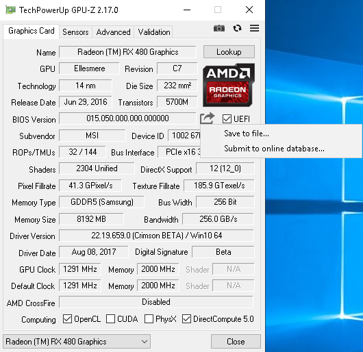 6GHz data rate) GDDR5 6GHz data rate) GDDR5 |
1242MHz (2484MHz data rate) GDDR3 |
|
Memory Bus Width |
384-bit |
384-bit |
256-bit |
512-bit |
|
Frame Buffer |
1.5GB |
1.5GB |
1GB |
1GB |
|
Transistor Count |
3B |
3B |
1.95B |
1.  4B 4B |
|
Manufacturing Process |
TSMC 40nm |
TSMC 40nm |
TSMC 40nm |
TSMC 55nm |
|
Price Point |
$499 |
~$420 |
~$190 |
Features:
Display Support:
| Maximum Digital Resolution | 2560×1600 |
| Maximum VGA Resolution | 2048×1536 |
| Standard Display Connectors | Mini HDMI Two Dual Link DVI |
| Multi Monitor | Yes |
| HDCP | Yes |
| HDMI4 | 1. 4a 4a |
| Audio Input for HDMI | Internal |
Standard Graphics Card Dimensions:
| Height | 4.376 inches (111 mm) |
| Length | 10.5 inches (267 mm) |
| Width | Dual-Slot |
Thermal and Power Specs:
| Maximum GPU Temperature (in C) | 97 C |
| Graphics Card Power (W) | 244 W |
| Minimum Recommended System Power (W) | 600 W |
| Supplementary Power Connectors | One 6-pin and One 8-pin |
Microsoft DirectX 11 Support
DirectX 11 GPU with Shader Model 5. 0 support designed for ultra high performance in the new API’s key graphics feature, GPU-accelerated tessellation.
NIVIDIA PhysX technology
GeForce GPU support for NVI DIA PhysX technology, enabling a totally new class of physical gaming interaction for a more dynamic and realistic experience with GeForce.
NVIDIA 3D Vision Ready
GeForce GPU support for NVIDIA 3D Vision, bringing a stereoscopic 3D experience to the PC. A combination of high-tech wireless glasses and advanced software, 3D Vision transforms hundreds of PC games into full stereoscopic 3D. In addi tion, you can watch 3D movies and 3D digital photographs in crystal-clear quality.
NVIDIA 3D Vision Surround Ready
Expand your games across three displays in full stereoscopic 3D for the ultimate «inside the game» with the power of NVIDIA 3D Vision and SLI technologies. NVIDIA Surround also supports triple screen gaming with non-stereo displays.
NIVIDIA CUDA Technology
CUDA technology unlocks the power of the GPU’s processor cores to accelerate the most demanding systems tasks – such as video transcoding – delivering incredible performance improvements over traditional CPU’s.
NVIDIA SLI Technology
Industry leading NVIDIA SLI technology offers amazing performance scaling for the world’s premier gaming solution.
32x Anti-aliasing Technology
Lightening fast, high-quality anti-aliasing at up to 32x sample rates obliterates jagged edges.
NVIDIA PureVideo HD Technology
The combination of high definition video decode acceleration and post-processing that delivers unprecedented picture clarity, smooth video, accurate colour, and precise image scaling for movies and video.
PCI Express 2.0 Support
Designed for the new PCI Express 2.0 bus architecture offering the highest data transfer speeds for the most bandwidth-hungry games and 3D applications, while maintaining backwards compatibility with existing PCI press motherboards for the broadest support.
Dual-link DVI Support
Able to drive industry’s largest and highest resolutionflat-panel displays up to 2560×1600 and with support for High-Bandwidth Digital Content Protection (HDCP).
HDMI 1.4a Support
Support for HDMI 1.4a including GPU accelerated Blu-ray 3D support, x.v.Color, HDMI Deep Color, and 7.1 digital surround sound.
Meet the Inno 3D GTX 580 OC
We have in our labs Inno3D’s implementation of the GTX 580, the Inno3D GTX 580 OC . As you realize, the card is an overclocked version of Nvidia’s design.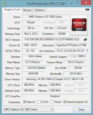 The card’s graphics clock and processor clock is boosted to 820 MHz/ 1640 MHz from the native 772 / 1544 MHz, while the memory runs at 1050 MHz
Here is some more information about the Inno3D GTX 580 OC, as the GPU-Z utility reports:
Nvidia’s GeForce GTX 580 graphics processor
As you may know, the GeForce GTX 480 had a troubled childhood. The GF100 chip that powered it was to be Nvidia’s first DirectX 11-class graphics processor, based on the ambitious new Fermi architecture. But the GF100 was famously tardy, hitting the market over six months after the competition’s Radeon HD 5000-series of DX11-capable chips. When it did arrive aboard the GTX 470 and 480, the GF100 had many of the hallmarks of a shaky semiconductor product: clock speeds weren’t as fast as we’d anticipated, power consumption and heat production were right at the ragged edge of what’s acceptable, and some of chip’s processing units were disabled even on the highest-end products. Like Lindsay Lohan, it wasn’t living up to its potential. When we first tested the GTX 480 and saw that performance wasn’t much better than the smaller, cooler, and cheaper Radeon HD 5870, we were decidedly underwhelmed.
Yet like Miss Lohan, the GF100 had some rather obvious virtues, including formidable geometry processing throughput and, as we learned over time, quite a bit of room for performance increases through driver updates. Not only that, but it soon was joined by a potent younger sibling with a different take on the mix of resources in the Fermi architecture, the GF104 chip inside the very competitive GeForce GTX 460 graphics cards.
Little did we know at the time, but back in February of this year, before the first GF100 chips even shipped in commercial products, the decision had been made in the halls of Nvidia to produce a new spin of the silicon known as GF110. The goal: to reduce power consumption while improving performance. To get there, Nvidia engineers scoured each block of the chip, employing lower-leakage transistors in less timing-sensitive logic and higher-speed transistors in critical paths, better adapting the design to TSMC’s 40-nm fabrication process.
At the same time, they made a few targeted tweaks to the chip’s 3D graphics hardware to further boost performance. The first enhancement was also included in the GF104, a fact we didn’t initially catch. The texturing units can filter 16-bit floating-point textures at full speed, whereas most of today’s GPUs filter this larger format at half their peak speed. The additional filtering oomph should improve frame rates in games where FP16 texture formats are used, most prominently with high-dynamic-range (HDR) lighting algorithms. HDR lighting is fairly widely used these days, so the change is consequential. The caveat is that the GPU must have the bandwidth needed to take advantage of the additional filtering capacity. Of course, the GF110 has gobs of bandwidth compared to most.
The second enhancement is unique to GF110: an improvement in Z-culling efficiency. Z culling is the process of ruling out pixels based on their depth; if a pixel won’t be visible in the final, rendered scene because another pixel is in front of it, the GPU can safely neglect lighting and shading the occluded pixel. More efficient Z culling can boost performance generally, although the Z-cull capabilities of current GPUs are robust enough that the impact of this tweak is likely to be modest.
The third change is pretty subtle. In the Fermi architecture, the shader multiprocessors (SMs) have 64KB of local data storage that can be partitioned either as 16KB of L1 cache and 48KB of shared memory or vice-versa. When the GF100 is in a graphics context, the SM storage is partitioned in a 16KB L1 cache/48KB shared memory configuration. The 48KB/16KB config is only available for GPU computing contexts. The GF110 is capable of running with a 48KB L1 cache/16KB shared memory split for graphics, which Nvidia says “helps certain types of shaders.”
Now, barely nine months since the chip’s specifications were set, the GF110 is ready to roll aboard a brand-new flagship video card, the GeForce GTX 580. GPU core and memory clock speeds are up about 10% compared to the GTX 480the GPU core is 772MHz, shader ALUs are double-clocked to 1544MHz, and the GDDR5 memory now runs at 4. 0 GT/s. All of the chip’s graphics hardware is enabled, and Nvidia claims the GTX 580’s power consumption is lower, too.
|
Peak pixel fill rate (Gpixels/s) |
Peak bilinear FP16 texel |
Peak memory bandwidth (GB/s) |
Peak shader (GFLOPS) |
Peak
rasterization rate (Mtris/s) |
|
| GeForce GTX 460 1GB 810MHz | 25.9 | 47.6 | 124. 8 8 |
1089 | 1620 |
| GeForce GTX 480 | 33.6 | 21.0 | 177.4 | 1345 | 2800 |
| GeForce GTX 580 | 37.1 | 49.4 | 192.0 | 1581 | 3088 |
| Radeon HD 5870 | 27.2 | 34.0 | 153.6 | 2720 | 850 |
| Radeon HD 5970 | 46. 4 4 |
58.0 | 256.0 | 4640 | 1450 |
On paper, the changes give the GTX 580 a modest boost over the GTX 480 in most categories that matter. The gain in FP16 filtering throughput, though, is obviously more prodigious. Add in the impact of the Z-cull improvement, and the real-world performance could rise a little more.
A question of balance
|
ROP pixels/ clock |
Textures
filtered/ clock int/fp16 |
Shader
ALUs |
Rasterized
triangles/ clock |
Memory
interface width (bits) |
|
| GF104 | 32 | 64/64 | 384 | 2 | 256 |
| GF100 | 48 | 64/32 | 512 | 4 | 384 |
| GF110 | 48 | 64/64 | 512 | 4 | 384 |
| Cypress | 32 | 80/40 | 1600 | 1 | 256 |
| Barts | 32 | 56/28 | 1120 | 1 | 256 |
Notably, other than the increase in FP16 filtering rate, the GF110 retains the same basic mix of graphics resources as the GF100.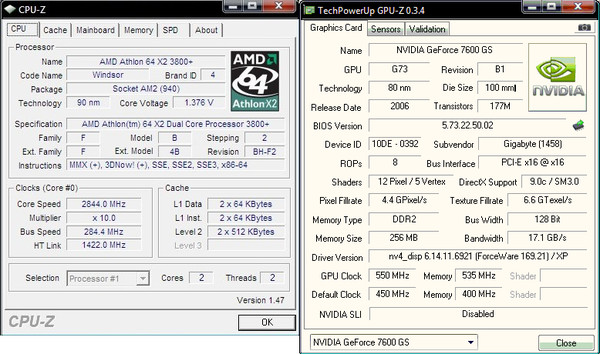 We’ll raise an eyebrow at that fact because the GF104 is arguably more efficient, yet it hits some very different notes. Versus GF100/110, the GF104’s ROP rate, shader ALUs, and memory interface width are lower by a third, the rasterization rate is cut in half, yet the texturing rate remains constant.
Not reflected in the tables above is another element: the so-called polymorph engines in the Fermi architecture, dedicated hardware units that handle a host of pre-rasterization geometry processing chores (including vertex fetch, tessellation/geometry expansion, viewport transform, attribute setup, and stream output). The GF104 has eight such engines, while the GF100/110 have 16. Only 15 of the 16 are enabled on the GTX 480, while the GTX 580 uses them all, so it possesses even more geometry processing capacity than anything to come before. (If you want to more fully understand the configuration of the different units on the chip and their likely impact on performance, we’d refer you to our Fermi graphics architecture overview for the requisite diagrams and such.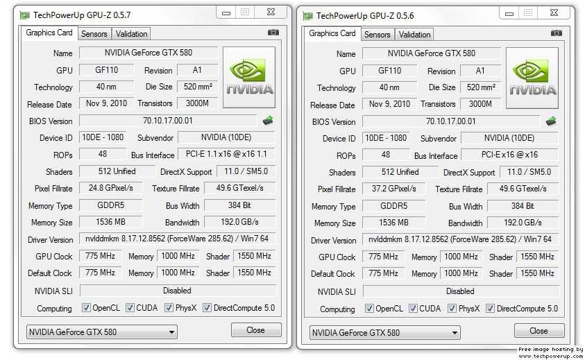 Nearly everything we said about the GF100 still applies to the GF110.)
Also still kicking around inside of the GF110 are the compute-focused features of the GF100, such as ECC protection for on-chip storage and the ability to handle double-precision math at half the rate of single-precision. These things are essentially detritus for real-time graphics, and as a consequence of product positioning decisions, GTX 580’s double-precision rate remains hobbled at one-quarter of the chip’s peak potential.
The GF110 hides under a metal cap that’s annoyingly tough to remove
We detected some trepidation on Nvidia’s part about the reception the GF110 might receive, given these facts. After all, there was a fairly widespread perception that GF100’s troubles were caused at least in part by two things: its apparent dual focus on graphics and GPU computing, and its clear emphasis on geometry processing power for graphics. The GF104’s singular graphics mission and improved efficiency in current games only fed this impression.
Nvidia’s counter-arguments are worth hearing, though. The firm contends that any high-end GPU like this one has plenty of throughput to handle today’s ubiquitous console ports, with their Unreal engine underpinnings and all that entails. The GF110’s relative bias toward geometry processing power is consistent with Nvidia’s vision of where future games based on DirectX 11 should be headedwith more complex models, higher degrees of tessellation, and greater geometric realism. In fact, Drew Henry, who runs Nvidia’s GeForce business, told us point blank that the impetus behind the GF110 project was graphics, not GPU computing products. That’s a credible statement, in our estimation, because the GF100-based Tesla cards have essentially zero competition in their domain, while the GeForces will face a capable foe in AMD’s imminent Cayman GPU.
Our sense is that, to some extent, the GF110’s success will depend on whether game developers and end users are buying what Nvidia is selling: gobs and gobs of polygons. If that’s what folks want, the GF110 will deliver in spades. If not, well, it still has 50% more memory bandwidth, shader power, and ROP throughput than the GF104, making it the biggest, baddest GPU on the planet by nearly any measure, at least for now.
The card and cooler
|
GPU clock (MHz) |
Shader ALUs |
Textures
filtered/ clock |
ROP pixels/ clock |
Memory
transfer rate |
Memory
interface width (bits) |
Peak
power draw |
Suggested
e-tail price |
|
| GeForce GTX 580 | 772 | 512 | 64 | 48 | 4. 0 Gbps 0 Gbps |
384 | 244W | $499.99 |
Amazingly, I’ve put enough information in the tables, pictures, and captions on this page that I barely have to write anything. Crafty, no? We’ve already given you some of the GTX 580’s vitals on the previous page, but the table above fills out the rest, including the $500 price tag. Nvidia expects GTX 580 cards to be selling at online retailers for that price starting today.
Gone are the quad heatpipes and exposed heatsink of the GTX 480 (left),
replaced by a standard cooling shroud on the GTX 580 (right).
Outputs include two dual-link DVI ports and a mini-HDMI connector.
Dual SLI connectors threaten three-way SLI.
The card is 10.5″ long.
Power inputs include one six-pin connector and one eight-pin one.
Although we didn’t find it to be especially loud in a single-card config, the GeForce GTX 480 took some criticisms for the noise and heat it produced.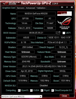 The noise was especially a problem in SLI, when the heat from two cards together had to be dissipated. Nvidia has responded to that criticism by changing its approach on several fronts with the GTX 580. For one, the end of the cooling shroud, pictured above, is angled more steeply in order to allow air into the blower.
Rather than using quad heatpipes, the GTX 580’s heatsink has a vapor chamber in its copper base that is purported to distribute heat more evenly to its aluminum fins. Meanwhile, the blades on the blower have been reinforced with a plastic ring around the outside. Nvidia claims this modification prevents the blades from flexing and causing turbulence that could translate into a rougher sound. The GTX 580 also includes a new adaptive fan speed control algorithm that should reduce its acoustic footprint.
The newest GeForce packs an additional power safeguard, as well. Most GeForces already have temperature-based safeguards that will cause the GPU to slow down if it becames too hot.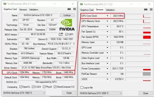 The GTX 580 adds a power monitoring capability. If the video card is drawing too much current through the 12V rails, the GPU will slow down to keep itself within the limits of the PCIe spec. Amusingly, this mechanism seems to be a response to the problems caused almost solely by the FurMark utility. According to Nvidia, outside of a few apps like that one, the GTX 580 should find no reason to throttle itself based on power delivery.
So who’s the competition?
AMD’s decision a couple of years ago to stop making really large GPUs and instead address the high-end video card market with multi-GPU solutions makes sizing up the competition for the GTX 580 a little bit complicated. We have some candidates, though, with various merits.
If you’re insistent on a single-GPU solution, Asus’ Republic of Gamers Matrix 5870 might be your best bet. This card has 2GB of GDDR5 memory, double that of the standard Radeon HD 5870, and runs at 894MHz, or 44MHz higher than AMD’s stock clocks for the Radeon HD 5870. That’s a modest bump in clock frequency, but Asus has given this card a host of overclocking-centric features, so the user can take it up from there. The ROG Matrix 5870 lists for $499.99 at Newegg, although it’s currently out of stock. We’ve included this card in our test results on the following pages, though it’s looking a little dated these days.
AMD’s true high-end solution is the Radeon HD 5970, pictured above. With dual Cypress GPUs, the 5970 is pretty much a performance titan. The 5970 has always been something of a strange specimen, for various reasons, including the fact that it has been incredibly scarce, and thus pricey, for much of the time since its introduction late last year. The card itself is incredibly long at 12.16″, ruling it out of an awful lot of mid-sized PC enclosures. As a dual-GPU solution based on AMD’s CrossFireX technology, the 5970 has the same potential for compatibility headaches and performance scaling pitfalls as a dual-card CrossFireX config. Also, the 5970 isn’t quite as fast as dual Radeon HD 5870s. Instead, it leaves some of its performance potential on the table, because its clock rates have been held down to keep power consumption in check. If your PSU can handle it, though, AMD expects the 5970 to reach dual-5870 clock speeds with the aid of a third-party overclocking tool with voltage control.
Oddly enough, the 5970 emerged from obscurity in the past week, when AMD notified us of the availability of cards like this Sapphire 5970 at Newegg at a new, lower price. Not coincidentally, that price is $499.99just the same as the GeForce GTX 580. There’s a $30 mail-in rebate attached, too, for those who enjoy games of chance. That’s a heckuva welcome for Nvidia’s latest, don’t you think?
We tested the 5970 at it stock speed, and in hindsight, perhaps we should have tested it overclocked to dual 5870 speeds, as well, since that’s part of its appeal. However, we had our eyes set on a third, more interesting option.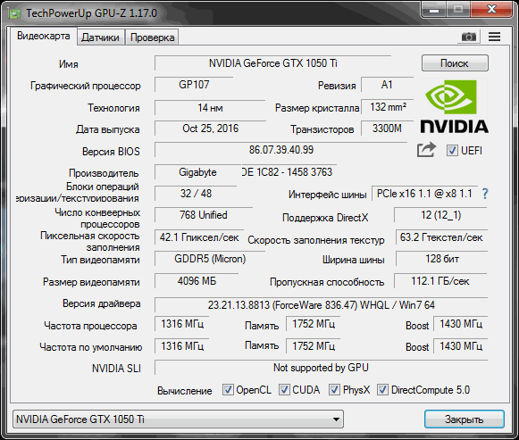
The introduction of the Radeon HD 6870 largely obsoleted the Radeon HD 5870, and we’d argue that a pair of 6870 cards might be AMD’s best current answer to the GTX 580. Gigabyte’s version of the 6870 is going for $244.99 at Newegg. (You can grab a 6870 for $239 if you’re willing to try your luck with PowerColor or HIS.) Two of these cards will set you back about as much as a single GTX 580. If you have the expansion slot real estate and PSU leads to accommodate them, they might be a good pick. Heck, they’re what we chose for the Double-Stuff build in our most recent system guide.
Naturally, we’ve tested both single- and dual-6870 configurations, along with some in-house competition for the GTX 580 in the form of a pair of GeForce GTX 460 1GB cards clocked at over 800MHz. These GTX 460 cards are the most direct competitors for the 6870, as well.
Our testing methods
Many of our performance tests are scripted and repeatable, but for some of the games, including Battlefield: Bad Company 2, we used the Fraps utility to record frame rates while playing a 60-second sequence from the game. Although capturing frame rates while playing isn’t precisely repeatable, we tried to make each run as similar as possible to all of the others. We raised our sample size, testing each FRAPS sequence five times per video card, in order to counteract any variability. We’ve included second-by-second frame rate results from Fraps for those games, and in that case, you’re seeing the results from a single, representative pass through the test sequence.
As ever, we did our best to deliver clean benchmark numbers. Tests were run at least three times, and we’ve reported the median result.
Our test systems were configured like so:
| Processor | Core i7-965 Extreme 3.2GHz |
| Motherboard | Gigabyte EX58-UD5 |
| North bridge | X58 IOH |
| South bridge | ICh20R |
| Memory size | 12GB (6 DIMMs) |
| Memory type | Corsair Dominator CMD12GX3M6A1600C8
DDR3 SDRAM at 1600MHz |
| Memory timings | 8-8-8-24 2T |
| Chipset drivers | INF update 9. 1.1.1025 1.1.1025
Rapid Storage Technology 9.6.0.1014 |
| Audio | Integrated ICh20R/ALC889A
with Realtek R2.51 drivers |
| Graphics | |
| Asus Radeon HD 5870 1GB with Catalyst 10.10c drivers |
|
| Asus ROG Matrix Radeon HD 5870 2GB with Catalyst 10.10c drivers |
|
| Radeon HD 5970 2GB with Catalyst 10.10c drivers |
|
| XFX Radeon HD 6870 1GB with Catalyst 10.10c drivers |
|
| Sapphire Radeon HD 670 1GB + XFX Radeon HD 6870 1GB with Catalyst 10. |
|
| MSI Hawk Talon Attack GeForce GTX 460 1GB 810MHz with ForceWare 260.99 drivers |
|
| MSI Hawk Talon Attack GeForce GTX 460 1GB 810MHz + EVGA GeForce GTX 460 FTW 1GB 850MHz with ForceWare 260.99 drivers |
|
|
Galaxy GeForce GTX 470 1280MB GC
with ForceWare 260.99 drivers |
|
|
GeForce GTX 480 1536MB
with ForceWare 260.99 drivers |
|
|
GeForce GTX 580 1536MB
with ForceWare 262.99 drivers |
|
| Hard drive | WD RE3 WD1002FBYS 1TB SATA |
| Power supply | PC Power & Cooling Silencer 750 Watt |
| OS | Windows 7 Ultimate x64 Edition
DirectX runtime update June 2010 |
 10c drivers
Thanks to Intel, Corsair, Western Digital, Gigabyte, and PC Power & Cooling for helping to outfit our test rigs with some of the finest hardware available. AMD, Nvidia, and the makers of the various products supplied the graphics cards for testing, as well.
Unless otherwise specified, image quality settings for the graphics cards were left at the control panel defaults. Vertical refresh sync (vsync) was disabled for all tests.
We used the following test applications:
- D3D RightMark beta 4
- Unigine Heaven 2.1
- ShaderToyMark 0.1.0
- TessMark 0.2.2.
- 3DMark Vantage 1.0.2
- Aliens vs. Predator benchmark
- Battlefield: Bad Company 2
- HAWX 2
- DiRT 2
- Left 4 Dead 2
- Sid Meier’s Civilization V
- Metro 2033
- StarCraft II
- Fraps 3.2.3
- GPU-Z 0.4.7
Some further notes on our methods:
-
We measured total system power consumption at the wall socket using a Yokogawa WT210 digital power meter. The monitor was plugged into a separate outlet, so its power draw was not part of our measurement.
 The cards were plugged into a motherboard on an open test bench.
The idle measurements were taken at the Windows desktop with the Aero theme enabled. The cards were tested under load running Left 4 Dead 2 at a 1920×1080 resolution with 4X AA and 16X anisotropic filtering. We test power with Left 4 Dead 2 because we’ve found that the Source engine’s fairly simple shaders tend to cause GPUs to draw quite a bit of power, so we think it’s a solidly representative peak gaming workload.
-
We measured noise levels on our test system, sitting on an open test bench, using an Extech 407738 digital sound level meter. The meter was mounted on a tripod approximately 10″ from the test system at a height even with the top of the video card.
You can think of these noise level measurements much like our system power consumption tests, because the entire systems’ noise levels were measured. Of course, noise levels will vary greatly in the real world along with the acoustic properties of the PC enclosure used, whether the enclosure provides adequate cooling to avoid a card’s highest fan speeds, placement of the enclosure in the room, and a whole range of other variables.
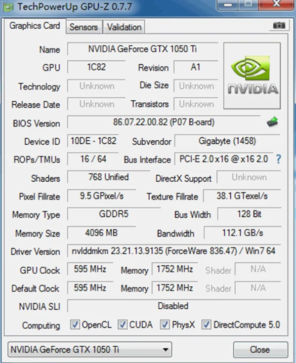 These results should give a reasonably good picture of comparative fan noise, though.
 - We used GPU-Z to log GPU temperatures during our load testing.
The tests and methods we employ are generally publicly available and reproducible. If you have questions about our methods, hit our forums to talk with us about them.
Power consumption
We’ll kick off our testing with power and noise, to see whether the GTX 580 lives up to its promise in these areas. Notice that the cards marked with asterisks in the results below have custom cooling solutions that may perform differently than the GPU maker’s reference solution.
The GTX 580’s power use when idling at the Windows desktop is quite reasonable for such a big chip. Our test system requires 13W less with a GTX 580 than with a GTX 480, a considerable drop. When we fire up Left 4 Dead 2, a game we’ve found causes GPUs to draw quite a bit of power, then the GTX 580 pulls a little more juice than its predecessor.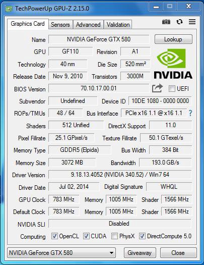 That’s not bad considering the higher clock rates and additional enabled units, but Nvidia claims the GTX 580 draws less power than the 480, even at peak.
When we asked Nvidia what the story was, they suggested we try a DX11-class workload, such as the Unigine Heaven demo, to see the difference between the GTX 480 and GTX 580. So we did:
Peak power draw is lower for both video cards, but the GTX 580 uses substantially less than the 480. Obviously, much depends on the workload involved. We may have to consider using multiple workloads for power testing going forward.
Noise levels and GPU temperatures
In spite of its relatively high peak power draw, the GTX 580 is among the quietest cards we tested. That’s a testament to the effectiveness of this card’s revised cooling design. Our positive impression of the cooler is further cemented by the fact that the GTX 580 runs 10°C cooler than the GTX 480, though its power use is comparable. The Radeon HD 5970 draws slightly less power than the GTX 580 but runs hotter and generates substantially more noise.
We do have some relatively boisterous contestants lined up here. MSI has tuned its dual-fan cooler on the GTX 460 to shoot for very low GPU temperatures, making it rather noisy. That dynamic gets worse when we slap another card next to it in SLI, blocking the intake for both fans. GPU temperatures shoot up to match the rest of the pack, and noise levels climb to a dull roar. Unfortunately, many GTX 460 cards have similar custom coolers that don’t fare well in SLI. The Radeon HD 6870’s blower is a better bet for multi-GPU use, but it’s still rather loud, especially for a single-card config. Cards that draw substantially more power are quieter and run at comparable temperatures.
Pixel fill and texturing performance
|
Peak pixel fill rate (Gpixels/s) |
Peak bilinear integer texel |
Peak bilinear FP16 texel |
Peak memory bandwidth (GB/s) |
|
| GeForce GTX 460 1GB 810MHz | 25. 9 9 |
47.6 | 47.6 | 124.8 |
| GeForce GTX 470 GC | 25.0 | 35.0 | 17.5 | 133.9 |
| GeForce GTX 480 | 33.6 | 42.0 | 21.0 | 177.4 |
| GeForce GTX 580 | 37.1 | 49.4 | 49.4 | 192.0 |
| Radeon HD 5870 | 27. 2 2 |
68.0 | 34.0 | 153.6 |
| Radeon HD 6870 | 28.8 | 50.4 | 25.2 | 134.4 |
| Radeon HD 5970 | 46.4 | 116.0 | 58.0 | 256.0 |
We’ve already looked at some of the theoretical peak numbers above, but we’ve reiterated them here a little more fully. These figures aren’t destiny for a video card. Different GPU architectures will deliver on their potential in different ways, with various levels of efficiency. However, these numbers do matter, especially among chips with similar architectural DNA.
You’d think 3DMark’s color fill rate test would track with the first column of scores above, but it turns out delivered performance is more directly affected by memory bandwidth. That’s why, for instance, the Radeon HD 6870 trails the 5870 here, in spite of a higher ROP rate. The GTX 580 is the fastest single-GPU solution, though it can’t keep up with the similarly priced multi-GPU options.
We’ve shunned 3DMark’s texture fill test recently because it doesn’t involve any sort of texture filtering. That’s tragic and sad, since texture filtering rates are almost certainly more important than sampling rates in the grand scheme of things. Still, this is a decent test of FP16 texture sampling rates, so we’ll use it to consider that aspect of GPU performance. Texture storage is, after all, essentially the way GPUs access memory, and unfiltered access speeds will matter to routines that store data and retrieve it without filtering.
AMD’s samplers are very fast indeed, as the Radeon HD 6870 keeps pace with Nvidia’s biggest, baddest GPU.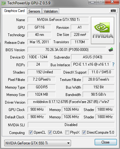 The Radeon HD 5970 is more than twice as fast in this specific case.
Here’s a more proper test of texture filtering, although it’s focused entirely on integer texture formats, not FP16. Texture formats like these are still widely used in games.
AMD’s texture filtering hardware is generally quite a bit faster than Nvidia’s with integer formats. The deficit narrows as we move to higher quality filtering levels, but the year-old Radeon HD 5870 remains faster than the GeForce GTX 580.
Happily, after struggling in the dark for a while, we finally have a proper test of FP16 filtering rates, courtesy of the guys at Beyond3D. Nvidia says the GF104 and GF110 can filter FP16 textures are their full rates rather than half. What kind of performance can they really achieve?
The GTX 580 comes pretty darned close to its theoretical peak rate, and it’s nearly twice the speed of the Radeon HD 5870. That quite the reversal. The GeForce GTX 460 moves up the chart, too, but doesn’t come anywhere near as close as the GTX 580 to reaching its peak potential. The GTX 580’s additional memory bandwidth and larger L2 cache50% better on both frontslikely account for the difference in delivered performance.
Shader performance
Peak shader (GFLOPS) |
Peak
rasterization rate (Mtris/s) |
Peak memory bandwidth (GB/s) |
|
| GeForce GTX 460 1GB 810MHz | 1089 | 1620 | 124.8 |
| GeForce GTX 470 GC | 1120 | 2500 | 133. |
| GeForce GTX 480 | 1345 | 2800 | 177.4 |
| GeForce GTX 580 | 1581 | 3088 | 192.0 |
| Radeon HD 5870 | 2720 | 850 | 153.6 |
| Radeon HD 6870 | 2016 | 900 | 134.4 |
| Radeon HD 5970 | 4640 | 1450 | 256. |
In recent months, our GPU reviews have been missing a rather important element: tests of GPU shader performance or processing power outside of actual games. Although some of today’s games use a fairly rich mix of shader effects, they also stress other parts of the GPU at the same time. We can better understand the strengths and weakeness of current GPU architectures by using some targeted shader benchmarks. The trouble is: what tests are worth using?
Fortunately, we have several answers today thanks to some new entrants. The first of those is ShaderToyMark, a pixel shader test based on six different effects taken from the nifty ShaderToy utility. The pixel shaders used are fascinating abstract effects created by demoscene participants, all of whom are credited on the ShaderToyMark homepage. Running all six of these pixel shaders simultaneously easily stresses today’s fastest GPUs, even at the benchmark’s relatively low 960×540 default resolution.
You may be looking between the peak arithmetic rates in table at the top of the page and the results above and scratching your head, but the outcome will be no surprise to those familiar with these GPU architectures. The vast SIMD arrays on AMD’s chips do indeed have higher peak theoretical rates, but their execution units can’t always be scheduled as efficiently as Nvidia’s. In this case, the GTX 580 easily outperforms the single-GPU competition. Unfortunately, this test isn’t multi-GPU compatible, so we had to leave out those configs.
Incidentally, this gives us our first good look at the shader performance differences between the Radeon HD 5870 and 6870. The 6870 is based on the smaller Barts GPU and performs nearly as well as the 5870 in many games, but it is measurably slower in directed tests, as one might expect.
Up next is a compute shader benchmark built into Civilization V. This test measures the GPU’s ability to decompress textures used for the graphically detailed leader characters depicted in the game. The decompression routine is based on a DirectX 11 compute shader. The benchmark reports individual results for a long list of leaders; we’ve averaged those scores to give you the results you see below.
These results largely mirror what we saw above in terms of relative performance, with the added spice of multi-GPU outcomes. Strangely, the Radeon HD 5970 stumbles a bit here.
Finally, we have the shader tests from 3DMark Vantage.
Clockwise from top left: Parallax occlusion mapping, Perlin noise,
GPU cloth, and GPU particles
These first two tests use pixel shaders to do their work, and the Radeons fare relatively well in both. The Perlin noise test, in particular, is very math intensive, and this looks to be a case in which the Radeons’ stratospheric peak arithmetic rates actually pay off.
These two tests involve simulations of physical phenomena using vertex shaders and the DirectX 10-style stream output capabilities of the GPUs. In both cases, the GeForces are substantially faster, with the GTX 580 again at the top of the heap.
Geometry processing throughput
The most obvious area of divergence between the current GPU architectures from AMD and Nvidia is geometry processing, which has become a point of emphasis with the advent of DirectX 11’s tessellation feature. Both GPU brands support tessellation, which allows for much higher geometric detail than usual to be generated and processed on the GPU. The extent of that support is the hot-button issue. With Fermi, Nvidia built the first truly parallel architecture for geometry processing, taking one of the last portions of the graphics pipeline that was processed serially and distributing it across multiple hardware units. AMD took a more traditional, serial approach with less peak throughput.
We can measure geometry processing speeds pretty straightforwardly with a couple of tools. The first is the Unigine Heaven demo. This demo doesn’t really make good use of additional polygons to increase image quality at its highest tessellation levels, but it does push enough polys to serve as a decent synthetic benchmark.
Notice that the multi-GPU solutions scale nicely in terms of geometry processing power; the alternate-frame rendering method most commonly used for load balancing between GPUs offers nearly perfect scaling on this front. Even so, the GTX 580 is still roughly a third faster than the Radeon HD 5970. Among the AMD solutions, only the dual Radeon HD 6870s can challenge the GTX 580 here, in part because of some tessellation optimizations AMD put into the Barts GPU.
TessMark’s multiple tessellation levels give us the chance to push the envelope even further, down to, well, insanely small polygons, and past the Radeons’ breaking point. This vast difference in performance once polygon counts get to a certain level will help inform our understanding of some important issues ahead. We can already see how Nvidia’s architectural choices have given the GTX 580 a distinct advantage on this front.
HAWX 2
Now we enter into disputed territory, and in doing so, we put some of those architectural differences we’ve discussed into play. The developers of HAWX 2 have made extensive use of DirectX 11 tessellation for the terrain in this brand-new game, and they’ve built a GPU benchmark tool based on the game, as well. HAWX 2 is slated for release this coming Friday, and in advance of that, Nvidia provided us with a stand-alone copy of the benchmark tool. We like to test with new games that take advantage of the latest features, but we’ve been hearing strong objections to the use of this gamefrom none other than AMD. Here’s AMD’s statement on the matter, first released prior to the introduction of the Radeon HD 6800 series and then sent out to us again yesterday:
It has come to our attention that you may have received an early build of a benchmark based on the upcoming Ubisoft title H.A.W.X. 2. I’m sure you are fully aware that the timing of this benchmark is not coincidental and is an attempt by our competitor to negatively influence your reviews of the AMD Radeon HD 6800 series products.
We suggest you do not use this benchmark at present as it has known issues with its implementation of DirectX 11 tessellation and does not serve as a useful indicator of performance for the AMD Radeon HD 6800 series. A quick comparison of the performance data in H.A.W.X. 2, with tessellation on, and that of other games/benchmarks will demonstrate how unrepresentative H.A.W.X. 2 performance is of real world performance.
AMD has demonstrated to Ubisoft tessellation performance improvements that benefit all GPUs, but the developer has chosen not to implement them in the preview benchmark. For that reason, we are working on a driver-based solution in time for the final release of the game that improves performance without sacrificing image quality. In the meantime we recommend you hold off using the benchmark as it will not provide a useful measure of performance relative to other DirectX 11 games using tessellation.
Interesting, no? I don’t need to tell you that Nvidia objects. With six days to produce our Radeon HD 6800 series review, we simply didn’t have time to look at HAWX 2 back then. I’m not sure we can come up with a definitive answer about who’s right, because that would require more knowledge about the way future games will use tessellationand we won’t know that until, you know, later. But we can explore some of the issues briefly.
Without tessellation, the mountains’ silhouettes are simple and straight
With tessellation, they’re much more complex
First, above is a close-up look at the impact of HAWX 2‘s tessellation on some of the mountains over which the entire benchmark scene takes place. This is just a small portion of a higher-resolution screen capture that hasn’t been resized. Clearly, tessellation adds tremendous complexity to the shape of the mountains.
Click the image for a larger version
Above are some images, provided by Nvidia, that reveal the sort of geometric complexity involved in this scene. The lower shot, in wireframe mode, gives us a sense of the polygon sizes. Unfortunately, these images were obviously resized by Nvidia before they came to us, so we can’t really estimate the number of pixels per polygon by looking at them. Still, we have a clear sense that many, many polygons are in usemore than most of today’s games.
Is this an egregious overuse of polygons, as AMD contends? I’m not sure, but I’d say it’s less than optimal, for a few reasons. One oddity is demonstrated, albeit poorly, in the image on the right. Although everything is turned at a nearly 45° angle, what you’re seeing at the center of the picture is something important: essentially flat ground. That flat surface is covered with large number of polygons, all finely subdivided into a complex mesh. A really good dynamic tessellation algorithm wouldn’t find any reason to subdivide a flat area into so many triangles. We’ve seen such routines in operation before, or we wouldn’t know to point this out. And there’s a fair amount of flat ground in the HAWX 2 benchmark map, as shown between the mountains in the image below.
Click the image for the full-sized version
The scene above shows us another potential issue, too, which is especially apparent in the full-resolution screenshot: the silhouettes of the mountains off in the distance appear to be just as jagged and complex as those up close, yet the texture resolution on those distant peaks is greatly reduced. Now, there are reasons to do things this wayincluding, notably, the way light behaves as it’s being filtered through the atmospherebut a more conventional choice would be to use dynamic LOD to reduce both the texture resolution and geometric complexity of the far-away peaks.
Finally, although close-up mountains in HAWX 2 look amazing and darn-near photorealistic, very little effort has been spent on the hostile airplanes in the sky. The models have very low poly counts, with obvious polygon edges visible. The lighting is dead simple, and the surfaces look flat and dull. Again, that’s an odd choice.
For its part, Nvidia freely acknowledged the validity of some of our criticisms claimed the game’s developers had the final say on what went into it. Ubisoft, they said, took some suggestions from both AMD and Nvidia, but refused some suggestions from them both.
On the key issue of whether the polygon counts are excessive, Nvidia contends Ubisoft didn’t sabotage its game’s performance on Radeon hardware. Instead, the developers set their polygon budget to allow playable frame rates on AMD GPUs. In fact, Nvidia estimates HAWX 2 with tessellation averages about 18 pixels per polygon. Interestingly, that’s just above the 16 pixel/polygon limit that AMD Graphics CTO Eric Demers argued, at the Radeon HD 6800 series press day, is the smallest optimal polygon size on any conventional, quad-based GPU architecture.
With all of these considerations in mind, let’s have a look at HAWX 2 performance with DX11 terrain tessellation enabled.
Having seen these tests run, I’d say we’re getting fluid enough frame rates out of all of the cards to keep the game playable. The GeForces are much faster, though, which you might have guessed.
We don’t have any great lessons to draw from all of this controversy, but we hope you understand the issues a little better, at least. We expect to see more skirmishes of this type in the future, especially if AMD’s Cayman GPU doesn’t move decidedly in the direction of higher polygon throughput. We’re also curious to see exactly how AMD addresses this one via its promised “driver-based solution” and whether or not that solution alters the game’s image quality.
Lost Planet 2
Our next stop is another game with a built-in benchmark that makes extensive use of tessellation, believe it or not. We figured this and HAWX 2 would make a nice bridge from our synthetic tessellation benchmark and the rest of our game tests. This one isn’t quite so controversial, thank goodness.
Without tessellation
Without tessellation
With tessellation
With tessellation
Here’s a quick look at the subject of this benchmark, a big, slimy slug/tank character from the game. Like a lot of other current games, LP2 has its DX11 effects tacked on in a few places, mostly in the level-end boss characters like this one. Tessellation adds some detail to the slug thing, mostly apparent in the silhouette of the its tail and its, uh, knees. Whatever they’re doing here works, because wow, that thing is creepy looking. I just don’t understand why the guts don’t ooze out immediately when the guys shoot it.
This benchmark emphasizes the game’s DX11 effects, as the camera spends nearly all of its time locked onto the tessellated giant slug. We tested at two different tessellation levels to see whether it made any notable difference in performance. The difference in image quality between the two is, well, subtle.
The Radeons don’t fare too poorly here, all things considered. The only solution that’s faster than the GeForce GTX 580 is a pair of 6870s in CrossFire, in fact. Unfortunately, the low clock speeds on the 5970’s individual GPUs keep it from performing as well as the 6870s in geometry-limited scenarios.
Civilization V
In addition to the compute shader test we’ve already covered, Civ V has several other built-in benchmarking modes, including two we think are useful for testing video cards. One of them concentrates on the world leaders presented in the game, which is interesting because the game’s developers have spent quite a bit of effort on generating very high quality images in those scenes, complete with some rather convincing material shaders to accent the hair, clothes, and skin of the characters. This benchmark isn’t necessarily representative of Civ V‘s core gameplay, but it does measure performance in one of the most graphically striking parts of the game. As with the earlier compute shader test, we chose to average the results from the individual leaders.
The Radeons pretty much clean up here, quite possibly due to their pixel shading prowess. The GTX 580 only manages to match the Radeon HD 5870.
Another benchmark in Civ V focuses, rightly, on the most taxing part of the core gameplay, when you’re deep into a map and have hundreds of units and structures populating the space. This is when an underpowered GPU can slow down and cause the game to run poorly. Unfortunately, this test doesn’t present its results in terms of frames per second. We can use the scores it produces to compare between video cards, but we can’t really tell whether performance will be competent based on these numbers alone. For what it’s worth, I’m pretty confident most of these cards are capable of producing tolerable frame rates at this very high resolution with 8X multisampling.
In this measure of actual gameplay performance, the GTX 580 comes in just behind the Radeon HD 5970. The only single-GPU solution that comes close is the GTX 480, and it’s more than 10% slower than the 580.
StarCraft II
Up next is a little game you may have heard of called StarCraft II. We tested SC2 by playing back a match from a recent tournament using the game’s replay feature. This particular match was about 10 minutes in duration, and we captured frame rates over that time using the Fraps utility. Thanks to the relatively long time window involved, we decided not to repeat this test multiple times, like we usually do when testing games with Fraps.
We tested at the settings shown above, with the notable exception that we also enabled 4X antialiasing via these cards’ respective driver control panels. SC2 doesn’t support AA natively, but we think this class of card can produce playable frame rates with AA enabledand the game looks better that way.
Once more, the GTX 580 is the fastest single-GPU solution, but it can’t quite catch the dual 6870s or GTX 460s. The Radeon HD 5970 struggles yet again, oddly enough, while the 6870 CrossFireX config performs quite well.
Battlefield: Bad Company 2
BC2 uses DirectX 11, but according to this interview, DX11 is mainly used to speed up soft shadow filtering. The DirectX 10 rendering path produces the same images.
We turned up nearly all of the image quality settings in the game. Our test sessions took place in the first 60 seconds of the “Heart of Darkness” level.
The GTX 480 is in a virtual tie with the Radeon HD 5870, and the GTX 580 breaks that deadlock. Still, all of the dual-GPU solutions are faster, including the Radeon HD 5970.
Metro 2033
This time around, we decided to test Metro 2033 at multiple image quality levels rather than multiple resolutions, because there’s quite a bit of opportunity to burden these GPUs simply using this game’s more complex shader effects. We used three different quality presets built into the game’s benchmark utility, with the performance-destroying advanced depth-of-field shader disabled and tessellation enabled in each case.
Interestingly, the Radeons grow relatively stronger as the complexity of the shader effects rises. By the time we reach the highest quality settings, the 5970 has matched the GTX 580and the dual 6870s are faster still.
Aliens vs. Predator
AvP uses several DirectX 11 features to improve image quality and performance, including tessellation, advanced shadow sampling, and DX11-enhanced multisampled anti-aliasing. Naturally, we were pleased when the game’s developers put together an easily scriptable benchmark tool. This benchmark cycles through a range of scenes in the game, including one spot where a horde of tessellated aliens comes crawling down the floor, ceiling, and walls of a corridor.
For these tests, we turned up all of the image quality options to the max, with two exceptions. We held the line at 2X antialiasing and 8X anisotropic filtering simply to keep frame rates in a playable range with most of these graphics cards.
Once more, the GTX 580 is the fastest single-GPU solution, supplanting the GTX 480 while solidly improving on its performance.
DiRT 2: DX9
This excellent racer packs a scriptable performance test. We tested at DiRT 2‘s “ultra” quality presets in both DirectX 9 and Direct X 11. The big difference between the two is that the DX11 mode includes tessellation on the crowd and water. Otherwise, they’re hardly distinguishable.
DiRT 2: DX11
When DiRT 2 is at its most strenuous, in the last few graphs above, the GTX 580 handily outperforms the GTX 480. This is one of the games where Nvidia says the GF110’s architectural enhancements, particularly the faster FP16 filtering, pay off.
Conclusions
On the whole, the GeForce GTX 580 delivers on much of what it promises. Power draw is reduced versus the GTX 480, at least at idle, and the card runs cooler while generating less noise than its predecessor. Performance is up substantially, between about 10 and 20%, depending on the application, which is more than enough to cement the GTX 580’s position as the fastest single-GPU graphics card on the planet.
We said earlier that the GTX 580’s competitive picture is a bit murky, but our test results have provided some additional clarity. The Radeon HD 5970 is faster than the GTX 580 across most games we tested, but we still don’t like its value proposition for several reasons. One of those reasons is the 5970’s relatively weak performance with high degrees of tessellation, a consequence of its low default clock speeds. The 5970 is also a very long card and relatively noisy.
Most of all, though, we simply prefer the option of grabbing a pair of Radeon HD 6870s. The 6870 CrossFireX setup was easily the best overall performer of any solution we tested across our suite of games. If you’re willing to live with the multi-GPU compatibility issues of the 5970, you might as well step up to two discrete cards for the same price. Heck, even though the 6870’s cooler isn’t very quiet, the dual 6870 config generated less noise under load than the 5970. We’re also much more comfortable with running two 6870s sandwiched together than we are with two of any flavor of GeForce GTX 460 we’ve yet seen. The custom coolers on various GTX 460 cards are often fine for single-card setups, but they mostly don’t play well with SLI.
With that said, we don’t entirely consider any current multi-card solution a truly direct competitor for the GeForce GTX 580. For one thing, the GTX 580 would make a heckuva building block for an SLI setup itself, and that would be one very powerful solution, likely with decent acoustics, too. (Note to self: test ASAP.) For another, we know that AMD’s Cayman GPU is coming very soon, and it should present more formidable competition for Nvidia’s new hotness.
In fact, we don’t yet have enough information to evaluate the GTX 580 properly just yet. This card is a nice advancement over the GTX 480, but is it improved enough to hold off Cayman? If the rumors are true, we may know the answer before the month is out.
Nvidia GTX 580 Overclocking Guide
Every time a new graphics card comes out, especially one based on a new architecture such as Nvidia’s GTX 580, early adopters and overclockers alike have to get over all sort of problems if they want to squeeze the maximum performance possible out of their brand spanking new GPU, so we are going t make this whole process a lot easier for all those of you GTX 580 owners out there that find themselves stuck in such a situation.
All the info that is shared in this article comes from Softpedia’s own experiments with the GTX 580, Nvidia’s graphics card making its way into our test labs just a few days ago.
For now we are going to limit ourselves to this overclocking tutorial as more info about the GTX 580 architecture as well as its performances will be covered in our review, that is bound to hit real soon.
But getting back to the matter at hand, the first thing that I am going to do is to take a quick look at the card’s default clocks to see where we stand.
As you can certainly see for yourself the GTX 580’s default core clock is set at 772MHz, its memory being clocked at 1002MHz (4008MHz data rate) while the shader clock runs at 1544MHz, being set at double the core’s frequency, as its the case with all Fermi based video cards.
As in the GF100, this can’t be altered by itself, so overclocking these cards is a matter of changing only two frequencies as well as the core’s voltage.
And here is where we came into our first hurdle with overclocking the GTX 580, as voltage tuning utilities that support Nvidia’s new GF110 core are really scarce at this time.
As a hardware reviewer, one runs into this sort of situations all the time, limited software support being one of the main reasons why overclocking results are not covered by every single review out there, especially when we are talking about new architectures that usually come with pre-production drivers and the like.
This is what happened to us when we reviewed the GTX 580 as well, and this is where the idea about writing such an GTX 580 overclocking guide came from, as most review sites out there don’t mention what tools they used in order to overclock, leaving early adopters to search for themselves the right tool for the job.
With this in mind, we set up to bring our users a quick guide that will enable them to unlock the full potential of the GTX 580, Nvidia’s card coming with an impressive overclocking headroom for an flagship product as you will most certainly see for yourself.
Pre-requisites
Before we start, the first thing to do is to download a few free tools from the Web, our main goal being to find a way of changing the core’s voltage without resorting to hardware modes and other stuff like that, the GF110 coming with a CHiL 8266 digital PWM controller which decides just how much juice the core needs.
As its the case with many other PWM controllers used in today’s top end graphics cards this can be also controlled via software, MSI Afterburner certainly being one of the most wide known tools available to overclockers worldwide.
Unfortunately, heading over to MSI’s Afterburner website and downloading these tools gets us the 2.0 version, this coming without voltage control support for the GTX 580 as I soon found out for myself when trying to overclock the card for the upcoming review.
There’s no need to worry though, beta versions of this tool are also available and usually come with support for the latest graphics cards out there.
Right now, the latest beta version is Afterburner 2.1 Beta 4, GTX 580 support making its way in the change log.
Another utility that supports the GTX 580 is Nvidia Inspector tool, this utility looking a lot like GPU-Z although it also comes with a really thorough overclocking panel, this being available for download from our website.
I recommend installing both of these tools and see what works best for you, Nvidia Inspector being also a really good alternative to GPU-Z, so you are really hitting two rabbits with one stone by going with this software.
The last tool that you need in your arsenal before getting to see what your GTX 580 is made off is the FurMark stress testing utility, available for download here.
Now that we got a hold of everything we need in order to overclock the GTX 580, its time for a small disclaimer as you need to understand Softpedia can’t be held reliable for what happens to your video card is anything goes wrong.
Furthermore, we do not encourage overclocking if you don’t know what you are doing, so please make sure you understand all the risks involved before getting started.
Another thing that I need to mention is this guide should also work for overclocking other Nvidia video cards, such as the GTX 480 and other Fermi based cards.
The overclocking process
I’ll assume that, by now, you have downloaded and installed all the utilities mentioned in the pre-requisite section, so we are going to get right into the action.
First thing to do now is to unlock voltage control and monitoring in MSI’s Afterburner tool by heading to the Settings tab found in the bottom right corner of the program’s main panel, the two check boxes needed being right under the General tab, in the Safety properties subsection, called Unlock Voltage Control and Unlock Voltage Monitoring, as you can see in the enclosed picture.
After clicking the OK button, you will get a message informing you these changes will be applied after restarting MSI’s utility, so do as informed.
After restarting the utility, check the Core Voltage slider found at the top of the main Afterburner panel, to see if this worked.
If it didn’t, there is another thing you can try as Afterburner saves all its settings in an config file that is found in the installation directory, called MSIAfterburner.cfg, the values that we are interested in being found in the [Settings] section, as UnlockVoltageControl and UnlockVoltageMonitoring.
Change both of these values to 1 and you are all set to go.
After saving the settings and starting Afterburner the Voltage Control slider should be unlocked.
If this is still not the case, you can resort to the Nvidia Inspector tool, this also allowing core voltage to be changed, although the GPU frequency slider was not available to me (if this were to be enabled you can pretty much give up on using Afterburner as this can do exactly the same things as MSI’s tool).
If this still doesn’t work or if, for whatever reason, you don’t want to change the GPU’s voltage, the GTX 580 can also be overclocked without a voltage increase, but you mileage may vary since the core’s frequency will most certainly be limited by the 1. 035V supplied to the GF110 core.
If you don’t seem to find the overclocking panel in Nvidia Inspector that is because there is a Show Overclocking/Hide Overclocking button that needs to be pressed in order to gain access to them.
For whatever reason, during my experiments, Nvidia Inspector and MSI Afterburner had different maximum voltages available, MSI’s tool featuring a whooping 1.3V, although every report out there, as well as Nvidia Inspector, said 1.138V is the maximum core voltage available through software for thr GTX 580.
A few more experiments showed this is indeed the case as raising the voltage over 1.138V in Afterburner had no result on the overclock achieved, Nvidia Inspector also reporting the voltage is set to 1.138V, so it’s safe to assume this is a bug that report the maximum available voltage wrong.
But moving past all that, with two overclocking tools at our disposal it’s time to crank the voltage all the way up to 1.138V and see where this takes us in terms of performance.
To find the maximum overclocking values for the graphics card, start by gradually increasing the core’s frequency (I recommend 25MHz increments if you are an overclocking noob).
After each increase fire up the FurMark stress testing program (I used MSI’s Kombustor utility but it’s basically the same thing as Kombustor is a redesigned FurMark), by just pressing the big GO! Button, the default settings being OK for testing the card’s stability.
I recommend doing this for about half an hour and if everything works well raise the core frequency once again.
You need to repeat these steps until you get artefacts in the rendered image, until Nvidia’s driver crashes or the computer freezes.
When this happens, don’t worry, as this simply means that you have gone too far and you need to take a slight step back.
Restart you computer and fire Nvidia Inspector and MSI Afterburner again, following the same steps as before, but when it comes to setting the core frequency go 10MHz lower than your last attempt and start FurMark yet again to see how things work out know.
If everything goes well for half an hour this means that you have come pretty close to your GTX 580 maximum core frequency (you can further fine tune it if you want), but if it doesn’t decrease the frequency yet again until you find the right value for you.
Now that you found the maximum frequency for your GPU is time to see what the memory chips hold in store, so repeat the whole process yet again, although this time increase your memory frequency instead of the core’s clock.
In my experiments, I managed to hit an impressive 920MHz for the core and 2100MHz for the memory, although I had to give up on raising the memory frequency further because of the limited time that I had at my disposal for this article, but if you have the time, I am sure these can go a lot higher, although is up to you to find just how high they can actually go.
End of it all, this speed increase got me a 10.4% increase in the overall 3DMark Vantage Performance score, a pretty nice boost for the small amount of work involved.
During this whole time, the fan was set to the auto setting, Nvidia’s GTX 580 cooling system being particularly efficient throughout my tests, although the system got pretty noise at times.
This is however a normal thing to happen since it had to blow out an increased amount of heat, the fan reving up just for a few seconds once in a while, quickly returning to its regular ear-friendly ways, something that we’ll cover in more detail in our upcoming review.
Until then I’ll leave you explore your GTX’s 580 overclocking potential, so please drop me a line and let my know how things worked out for you.
could have been better than GECID.com. Page 1
::>Video cards
>2019
> Gameplay testing of the NVIDIA GeForce GTX 580 video card in the realities of 2019: it could be better
09-05-2019
Page 1
Page 2
One page
In March 2010, the GeForce GTX 480 video card debuted, and in November it was replaced by the GeForce GTX 580. There were both external and internal reasons for such a rush. The first ones include the release of a worthy competitive Radeon HD 6800 series. But the main ones were internal problems — high power consumption and heat dissipation of the GTX 480, frequent breakdowns and a low percentage of good chips produced. Initially, the NVIDIA GF100 GPU was supposed to include all 16 SM blocks, but the company decided to lower the bar to 15 in order to sell more GPUs.
In turn, the GeForce GTX 580 received a modified GF110 chip with a full number of SM blocks, CUDA cores and texture modules. It uses the same Fermi microarchitecture, but with minor improvements that along the way made it possible to increase clock speeds by 8-10% and even slightly reduce power consumption. This had a positive effect on the overall level of performance, but the novelty did not bring any radically new technologies. The size of the video buffer at first also did not change, although later 3-gigabyte versions appeared.
We will evaluate the capabilities of this flagship using the MSI GeForce GTX 580 Lightning as an example. At one time we prepared a text review on it, but it did not stay with us. Therefore, we turned to colleagues from the Overclockers.ua website, who kindly provided it to us for testing.
This is the top version, which was also created for overclocking experiments. Therefore, she received a 16-phase power subsystem, overclocking tools for extreme overclocking, an improved element base and an efficient Twin Frozr III cooler. It consists of a massive base, three nickel-plated copper heat pipes, an aluminum heatsink, and two 90mm fans. In games, the GPU temperature did not exceed 63 ° with a critical indicator of 97 ° C.
The first surprise upon reacquaintance was waiting for us in the GPU-Z utility. At first glance, everything is fine: the GPU frequency is 8% higher than the standard, and the memory is 5% higher. But if you look closely, the program indicates the use of 8 PCIe 2. 0 lanes. They checked it on several test systems, but they did not see the required 16 lines.
This may be a GPU-Z glitch. But there was no time or desire to look for another GeForce GTX 580. And according to tests available online, the difference in performance between 8 and 16 lines is only a few percent. Therefore, even if the video card really works in x8 mode, then factory overclocking is enough to cover the difference. Thus, we can assume that we have a reference model on the test.
At one time, the MSI GeForce GTX 580 Lightning outperformed the overclocked GeForce GTX 480 by 10-18%. Let’s see if anything has changed since then and if the possible x8 mode had a big impact?
Rainbow Six: Siege with the medium preset in HD shows that there were no significant changes: the 580th is still 15-18% better than its predecessor. But, of course, it is impossible to judge by one benchmark, so let’s move on to the next one.
In Middle-earth: Shadow of War , the advantage of the GeForce GTX 580 reaches 25-28%. Here, the superiority of the GF110 over the GF100 in terms of the number of structural blocks and clock frequencies is already fully felt.
In The Crew 2 the advantage of the 580th is retained, but it is at the lowest level — 9-11%.
And finally in Far Cry 5 at a low preset, the 480th absolutely could not oppose its successor. Both suffered from a lack of video memory, but the performance of the GTX 580 was 16-20% higher.
Thus, even if this is not a GPU-Z glitch and the video card really worked in x8 mode, it is still 17-18% better than the GeForce GTX 480. Similar results were obtained in 2010, so we can safely move on to familiarization with the test stand and the main game testing.
The following stand was used for testing:
- Intel Core i7-7740X
- Thermaltake Water 3.
0 Riing RGB 240
- ASUS TUF X299 MARK 1
- 2 x 8 GB DDR4-2133 G.SKILL Sniper X
- Apacer PANTHER AS330 240 GB / 960 GB
- Seagate ST2000DX001 2TB
- Seasonic Snow Silent 1050 1050W
- Thermaltake Core P3
- AOC U2879VF
An external system with AVerMedia Live Gamer 4K was used to record gameplay in Full HD resolution, i.e. without loss of performance.
Traditionally, before the main test of a retro video card, we check how it is doing with driver support. The GTX 580 belongs to the Fermi family, so the latest WHQL driver for it was released in March 2018. As for the GeForce GTX 480.
Therefore, almost all the problems that were in the test of its predecessor have been preserved. That is, Battlefied V refused to launch at all, Forza Horizon 4 hurriedly crashed on Windows, there is no support for Vulkan at all, and Quake Champions just issued a warning, but still started. The only difference is that Fallout 4 immediately recognized the graphics card and offered medium graphics settings.
Otherwise there were no problems. This time, just over 20 games take part in the test. To save time, we decided not to launch the simplest ones, such as DOTA 2, Rocket League, Crossout and others. They started without problems on the 480th, so they would have gone with a bang here. And if you want to know their approximate frame rate, then add 16% to past results.
ZOTAC GeForce GTX 580 review and testing GECID.com. Page 1
::>Video cards
>2010
> ZOTAC ZT-50101-10P
11-17-2010
Page 1
Page 2
One page
Not so long ago we tested new models of video cards based on the improved Barts core manufactured by AMD. The Radeon HD 6870 and Radeon HD 6850 graphics processors are representatives of the middle price range of the new 6800 series, but the NVIDIA GeForce GTX 580 is positioned as the most productive single-chip solution. We will try to confirm or refute these lofty «claims» by conducting our own testing of the capabilities of the new video accelerator.
Video cards based on the GPU of the previous series NVIDIA GeForce GTX 480 were the best in performance among single-chip solutions for half a year. Such superiority of NVIDIA’s product over AMD’s Radeon HD 5870 could not be called absolute. In many applications, and especially in scenes requiring processing speed of tessellation algorithms, NVIDIA GeForce GTX 480 really was the leader. However, other parameters, such as power consumption, heat dissipation, price and noise of the video cards based on the NVIDIA GeForce GTX 480 were seriously inferior to the «top» solution Radeon HD 5870 from AMD. It is precisely because of the high power consumption that NVIDIA specialists have not yet been able to release a two-chip video card based on their «top» core based on the Fermi architecture. AMD engineers, having selected crystals with the lowest possible supply voltage, and therefore with minimal power consumption and heat pack, offered the public a dual-chip video card Radeon HD 5970. Even now it can still be called the most productive graphics accelerator.
The two main problems faced by NVIDIA engineers when releasing the GeForce GTX 480 chip are its high power consumption and low percentage of good chips in production. We will not single out one of these reasons as the main one, but as a result, users received a GeForce GTX 480 with an inferior core of the Fermi architecture. One of the 16 streaming multiprocessors (SM — Streaming Multiprocessors) in it was disabled at the factory. Such a move made it possible to increase the percentage of workable, but cut-down chips for GeForce GTX 480 video cards, and it also gave somewhat lower power consumption and reduced chip heating. Even with this cutback, the GeForce GTX 480 delivers performance that, in the vast majority of applications, outperforms its main competitor from AMD, the Radeon HD 5870 accelerator.
Now, after the release of the first accelerators of the new Radeon HD 6800 line and the imminent appearance of the «top» video cards of this series on the «Cayman» core and the two-chip «Antilles» solution, NVIDIA has dealt a preemptive blow to AMD by introducing an even more powerful GeForce solution to the market. GTX 580. In fact, with a few exceptions, the GeForce GTX 580 video card is a modified and improved version of the GeForce GTX 480. It has a full set of streaming multiprocessors (16 pieces), a slightly reduced heat pack and power consumption against the background of increased operating frequencies. This combination of features gives a significant superiority of the new GeForce GTX 580 over its predecessor.
The conquest of the market of «top» solutions by NVIDIA strongly depends on the pricing of products in this niche from AMD’s direct competitor. The GeForce GTX 580 video card is offered for sale at a price of $500, while the cost of the «top» accelerator from AMD Radeon HD 5870 has already dropped to $330. If we talk about our market, then prices can be roughly predicted: AMD Radeon HD 5870 sells for $380 on average, GeForce GTX 580 is expected to cost $600 and AMD Radeon HD 5970 sells for $650 on average. The price ladder is quite consistent with the performance of these video cards and their capabilities.
NVIDIA’s new GF110 core architecture for the GeForce GTX 580
It has already been said that the GF110 has become an improved modification of the GF100, and the number of changes is quite insignificant. Learn more about the architecture of the GeForce GTX 480 in the review of the ZOTAC GeForce GTX 480 video card. The die of both video cards has a 40-nm manufacturing process and contains more than 3 billion transistors.
The main goal in the changes to the GeForce GTX 580 die was to increase its total performance and computing power. Only two features of the core were redesigned — the FP16 filtering speed was doubled and the performance in the Z-cull invisible surface rejection algorithms was increased (new tile formats were introduced).
The GF110 GPU was able to filter the FP16 texture in one cycle, while its predecessor GF100 did it in two cycles. This will give a good boost in applications that are demanding on the texture performance of the accelerator.
The performance gain in hidden object culling will give the GF110 a better performance in overdraw applications and add efficiency to the available video accelerator memory bandwidth. According to NVIDIA, these two improvements will give a total increase in performance per clock, on average, up to 14%.
|
GeForce GTX 460 768MB |
GeForce GTX 460 1024MB |
GeForce GTX 470 |
GeForce GTX 480 |
GeForce GTX 580 |
|
|
GPU manufacturing process, nm |
40 |
||||
|
Graphics processing clusters, pcs. |
2 |
2 |
4 |
||
|
Number of Streaming Multiprocessors |
7 |
7 |
14 |
15 |
16 |
|
Number of CUDA cores |
336 |
336 |
448 |
480 |
512 |
|
Number of texture units |
56 |
56 |
56 |
60 |
64 |
|
Number of ROPs |
24 |
32 |
40 |
48 |
48 |
|
GPU frequency, MHz |
675 |
675 |
607 |
700 |
772 |
|
Frequency of CUDA cores, MHz |
1350 |
1350 |
1215 |
1401 |
1544 |
|
Effective video memory frequency, MHz |
3600 |
3600 |
3348 |
3696 |
4008 |
|
Video memory size, MB |
768 |
1024 |
1280 |
1536 |
1536 |
|
Memory bus width, bits |
192 |
256 |
320 |
384 |
384 |
|
DirectX support |
11 |
||||
|
Maximum TDP, W |
150 |
160 |
215 |
250 |
244 |
|
Recommended PSU power, W |
450 |
450 |
550 |
600 |
600 |
|
GPU temperature limit, °C |
104 |
104 |
105 |
105 |
97 |
|
Estimated cost in stores, $. |
~185 |
~230 |
~350 |
~490 |
over 499 |
The desire to achieve better energy efficiency indicators from the redesigned GF110 chip and increase the yield of working crystals during their production, forced the chip developers to make changes to the new core at the chip level. Various types of transistors were used in the design of the integrated circuit. In places less demanding on performance, transistors with low leakage currents, but with a greater delay, were used, and in other places with increased demands on performance, transistors with high leakage currents, but with increased speed. It was these changes that led to very significant power savings, which made it possible for NVIDIA to increase the core clock speeds by 72 MHz and enable the 16th SM streaming multiprocessor, which was disabled in the GF100 core used in the original GeForce GTX 480 design. One streaming multiprocessor carries 32 CUDA cores, four texture units and one PolyMorph geometry engine, all of which are available in the new edition of the core based on the Fermi design. If we compare the frequency formula of the GeForce GTX 480 (700/ 1401/ 924 MHz) with the GeForce GTX 580, then the latter has raised: the core frequency to 772 MHz, the shader frequency to 1544 MHz and the memory frequency to 1002 MHz, which is an effective frequency of 4008 MHz. Also GF110 now has 512 functional CUDA cores, 64 texture units and 16 PolyMorph engines.
The rest of the core content remained unchanged. There are six Raster Operation Sections (ROPs), each with a 64-bit memory bus, for a total of 384-bit memory bus. Each section computes eight 32-bit integer pixels per clock, for a total of 48 pixels per clock.
After describing the theoretical capabilities of the new GF110 core, let’s move on to the practical part of our review, describe the video card from ZOTAC based on the GeForce GTX 580 video processor that got into our laboratory. GeForce GTX 580 (ZT-50101-10P), presented on the manufacturer’s website:
|
Model |
ZOTAC GeForce GTX 580 (ZT-50101-10P) |
|
Graphics core |
NVIDIA GeForce GTX 580 (GF110-375-A1) |
|
Conveyors |
512 unified flow |
|
Supported APIs |
DirectX 11, OpenGL 4.1 |
|
Core frequency, MHz |
772 |
|
Frequency of unified processors, MHz |
1544 |
|
Memory frequency (effective), MHz |
1002 (4008) |
|
Size (type) of memory, MB |
1536 (GDDR5) |
|
Memory bus bit |
384 |
|
Tire standard |
PCI Express X16 2. |
|
Maximum resolution |
Up to 2560×1600 (Dual-link DVI) or 1920×1200 (Single-link DVI) |
|
Outputs |
2xDVI-I, mini HDMI |
|
HDCP and HD video support |
Yes |
|
Dimensions, mm |
111×267 |
|
Power Supply Power Requirements, Watts |
~600 |
|
Maximum allowable core temperature, ° |
97 |
|
Drivers |
Latest drivers can be downloaded from support page or GPU manufacturer website . |
|
Manufacturer website |
http://www.zotac.com/ |
According to the data in the table, you can see that there are not many differences between the reference solution ZOTAC GeForce GTX 480 and ZOTAC GeForce GTX 580. As already noted, the operating frequencies of the accelerator were changed, the number of stream pipelines became 512, the video card received support for OpenGL 4.1, and its critical operating temperature dropped to 97 °C. The dimensions of the board itself, the rear panel connectors, and the minimum power supply required for this accelerator to operate remain exactly the same as for the GeForce GTX 480. Note that the ZOTAC GeForce GTX 580 video card supports additional NVIDIA PureVideo HD Technology, NVIDIA 3D Vision Surround, NVIDIA PhysX technologies Technology, NVIDIA CUDA Technology and NVIDIA SLI Technology.
We have received a serial ZOTAC GeForce GTX 580 video card with a simple and typical box design for this manufacturer.
The packaging of the video card is black and yellow. On the front side of the cardboard box, the model of the video card, the amount of memory, its type and the bandwidth of the memory bus are indicated. There are also mentions of support for NVIDIA PhysX proprietary technologies and the presence of an HDMI connector. In the upper right corner, the manufacturer draws attention to the support of proprietary technologies: NVIDIA GeForce CUDA, NVIDIA PureVideo HD, NVIDIA SLI.
On the back of the box is a small overview of the capabilities of this video card. The advantages of using technologies are described: NVIDIA 3D Vision Surround and PhysX.
Filling of polygraphy is quite informative, the buyer can immediately learn about all the advantages and characteristics of the product he is purchasing.
The video card itself and additional delivery components are located inside. Together with the graphics accelerator, you can get the following:
-
User’s manual;
-
CD with software and drivers;
-
Disc with licensed version of Prince of Persia: The Forgotten Sands;
-
A sticker explaining how to power up the video card and warning about the accelerator getting too hot under load;
-
Video card power adapter from two 6-pin connectors to one eight-pin PCI Express;
-
Video card power adapter from two MOLEX connectors to one six-pin PCI Express;
-
DVI to VGA adapter;
-
Mini-HDMI to HDMI adapter.
I was a bit puzzled by the sticker with a warning about the hot surface of the video card at the time of its intensive use. It was exactly the same in the GeForce GTX 480 package, but the design of the cooling system of the latter did not cover most of the radiator with a plastic casing, on the surface of which you could really get burned. In the GeForce GTX 580, almost everything is covered with plastic, which protects the user from unpleasant moments of using the accelerator. I would like to note that the power adapters included in the package indicate the need to use a sufficiently powerful power supply, as it was said in the specification of at least 600 watts. This may cause some problems when choosing a configuration. In general, the equipment should fully compensate for all the nuances of installing this video card in a modern system unit.
The ZOTAC GeForce GTX 580 video card itself is made on a dark textolite, the front side of which is closed by a cooling system with a dark plastic casing.
The GeForce GTX 580 graphics card uses a printed circuit board of exactly the same overall dimensions as the GeForce GTX 480 — its length is 267 mm (10.5″), that is, about a centimeter shorter than the accelerators on the Radeon HD 5870, this can help it fit in almost any modern cabinet
Additional power (in addition to the PCI Express bus) requires one 6-pin and one 8-pin plug. NVIDIA claims that this card has a TDP of 244W, which is slightly less than its predecessor GeForce GTX 480 and significantly less than the Radeon HD 5970, which barely fits the PCI-SIG group’s 300W ceiling. Therefore, for the «top» solution, NVIDIA recommends a 600W power supply or higher. Also in the image above you can see two SLI ports. This will allow you to combine several similar video cards into one subsystem.
On the reverse side of the printed circuit board of the video card there is a GPU power system chip — a CHiL Semiconductor CHL8266 PWM controller using six phases. A similar one was used on the GeForce GTX 480 accelerator board.
There are three transistors for each power phase (one in the upper arm and two in the lower one). This approach allows you to better remove heat from the elements of the power subsystem.
The memory is powered by 1+1 phases (1 phase Vdd + 1 phase Vddq), controlled by Anpec APW7088 controller. In the GeForce GTX 580 graphics card, one dual-channel controller controls two video memory voltages Vdd and Vddq. Thus, in total we get a 6 + 2-phase power system for the ZOTAC GeForce GTX 580 video card.
We were a bit surprised by the use of hex star screws to secure the internal aluminum shroud of the graphics card. At the same time, the radiator itself and the plastic outer casing are fastened with ordinary screws for a Phillips screwdriver. Most likely, this was done as an additional protection against removal of the inner casing, which often sits quite firmly on the thermal interface. If it is inaccurately separated from the board, its elements can be damaged.
It is worth noting a fairly large number of tantalum capacitors used in the PCB filling. Particular attention can be paid to the four tantalum capacitors shown in the image above, they improve the GPU power scheme, as a result of which the temperature of the graphics core drops, compared to solutions based on the standard element base used in the GeForce GTX 480.
The board occupies two slots on the rear panel of the case. For a sufficiently voluminous cooling system, the user will have to free up space inside the case.
There are two DVI ports and one mini-HDMI on the interface panel. Plus, the second slot will be completely occupied by the exhaust grill, which blows heated air out of the system unit. Such a set of output interfaces, together with the adapters supplied, will give the user maximum versatility in connecting monitors and other image output devices.
The NVIDIA GeForce GTX 580 GPU installed here is marked GF110-375-A1.
The frequency scheme of the video card and other characteristics look like this: and shader domains at a frequency of 1544 MHz, respectively. Video memory received 1002 MHz real or 4008 MHz effective frequency.
The tested video card uses GDDR5 memory chips manufactured by SAMSUNG with a total capacity of 1536 MB. The K4G10325FE-HC04 marking indicates that these chips provide an access time of 0.4 ns, which corresponds to a real frequency of 1250 MHz or 5000 MHz effective and provides a significant headroom for overclocking.
Cooling system
Let’s take a closer look at the video card’s cooling system. It is completely devoid of heat pipes, which were used in the GeForce GTX 480.
The GeForce GTX 580’s new cooling design uses an evaporation chamber to effectively dissipate heat from the GPU. The heat coming from the GPU is transferred to the copper pad, which is the wall of the sealed compartment, which contains a liquid with a low boiling point. After reaching a certain temperature, the liquid changes its state of aggregation and turns into a gaseous one. Evenly distributed throughout the inner cavity of the pillow, gas molecules transfer heat to all its remote parts. From the copper cushion, heat is transferred to the aluminum radiator of the cooling system. Having lost the heat necessary for the gaseous state, the gas turns into a liquid, condensing on the walls of the pillow, and flows down through special pores in the copper walls to the starting point of evaporation. Then the cycle repeats again. The turbine-type fan installed in the cooling system drives cool air through the heated fins of the aluminum radiator and blows the heat out of the case.
From the GeForce GTX 480 cooling system, only an additional radiator plate remains here. It covers the upper part of the video card board and provides heat dissipation, through a special thermal interface, from the memory chips and transistors of the power system.
To reduce idle power consumption, the GF110 graphics chip is reduced to 50 MHz and the memory frequency to 67.5 MHz. Simultaneously with these actions, there is a decrease in the supply voltage on the GPU to 0.95 V. As a result, it turns out to significantly reduce the level of energy consumption during system inactivity. On our test bench, the power consumption of the ZOTAC GeForce GTX 580 was approximately the same as that of the ZOTAC GeForce GTX 480, i.e. at the level of 145 watts. Of course, it is logical that in terms of power consumption in idle mode, such a powerful video accelerator cannot compete with video cards of the middle or lower class. Therefore, on average, for video cards like the NVIDIA GeForce GTX 460 1GB GDDR5, the powerful NVIDIA GeForce GTX 580 loses about 20 watts.
Cooling Efficiency
At full load on the NVIDIA GeForce GTX 580, the total system power consumption was 445W. To create this stress mode, we used the OCCT GPU utility, rather than the more familiar FurMark . Since when using the latter, after half a minute, a new overload protection was observed, which was introduced by the manufacturer. As a result, system power consumption was reduced from 445W to 340W. Apparently, this technology has not yet been fully developed, since when working in a similar OCCT GPU utility, there was no reduction in power consumption.
Thanks to the unique cooling system with a vapor chamber, the temperature of the ZOTAC GeForce GTX 580 video card was reduced compared to the «reference» design video cards based on the GeForce GTX 480 chip. 100º, then on the GeForce GTX 580 the temperature rises only to 90 º, which already seems to be an achievement. Due to the fact that the efficiency of the new cooler was increased by an order of magnitude, this allowed the fan to operate at lower speeds with less noise. Despite the overall «hot temper» of the video card, the noise level of the ZOTAC GeForce GTX 580, even at maximum load, is not very high, but is in the region of average values. Moreover, in video games that load the graphics card less than the OCCT GPU stress test, the noise level can be completely described as below average. Therefore, for most gamers, the noise of the turbine of the new video card will definitely not cause inconvenience.
Related news «The author of GPU-Z found a way to disable protection against stress tests on the GeForce GTX 580» — NVIDIA WORLD
A way to warm up the video card to full using FurMark.
Fluffy bagels and cubes are now banned.
With the release of the new video card GeForce GTX 580, NVIDIA has joined AMD in the confrontation with utilities that warm up the graphics processor and the video card as a whole to the limit. According to the official statement, special chips are installed on the GeForce GTX 580 video cards that check the consumption currents along the +12 V power lines from the PCI-Express bus slot and power amplifiers. The NVIDIA driver checks the power consumption values and reduces the frequencies by 50% when it detects the launch of potentially dangerous applications, in particular the FurMark and OCCT stress tests, or when a certain power consumption limit is exceeded. This protection should not affect regular games. It is the work of protection that explains the strange readings of preliminary studies of the performance of the GTX 580 in FurMark.
The feasibility of such protection raises many questions. Firstly, studies of real power consumption show that some completely “legitimate” games and applications can cause no less or even more consumption than the same FurMark, for example: PixelShader test from 3DMark 06, Crysis Warhead DX10. Secondly, simply renaming the executable file of the «harmful» program may be enough to bypass the protection in the driver, moreover, it has already been confirmed that the protection does not work for older versions of FurMark. Thirdly, such measures increase the cost of video cards (three monitoring chips + strapping, seats, PCB tracks) and create potential driver stability problems — constant work with the i2c bus can be very expensive, as the authors of third-party utilities like RivaTuner have repeatedly seen.
But what’s done is done, and with the idea of stress testing cards at home, so useful for identifying manufacturing defects, as well as for finding the limits of overclocking, until you have to say goodbye. Undoubtedly, action will generate reaction, for example in the form:
- unofficial driver patches that remove protection, as was the case with SLI and PhysX;
- clever tricks in the next versions of utilities to cheat the driver;
- instructions for hardware «neutralization» of pest chips;
- increased demand for stealing NVIDIA’s internal test called MODS and integrating parts of it into utilities — the company won’t ban itself;
- the emergence of even more «deadly» methods of stress testing, for example, through the CUDA API.
We will cover the further course of the struggle between light and dark forces, and may the most worthy win!
drivermonitoringGeForce GTX 580FurMarkOCCT Perestroïkautilities
comment on similar news
Geeks3D
A new version of a small but informative utility.
New version 0.4.8 of the GPU-Z utility has the following changes:
- Added support for GeForce GTX 580, GT 420, GT440 and future variants based on GF104;
- updated formula for TMU count and scene fill rate with texturing;
- Fixed video memory frequency monitoring for AMD Radeon HD 6850 and 6870 video cards;
- Fixed CrossFire detection when using old ATI drivers;
- added siding for voltage monitoring on AMD graphics cards with non-standard VRM;
- PowerColor manufacturer detection corrected.
You can download the latest version of the program from the official site.
GeForce GTX 580GPU-Zutilities
comment on similar news
The closer the release of the GeForce GTX 580, the more information about its performance (of varying degrees of certainty) leaks to the Web. This time, a volley from four benchmarks at once.
3DMark Vantage, Extreme preset:
12871 points — quite consistent with early reports of 12700 points.
H.A.W.X. 2:
Unigine Heaven:
Here we have the promised advantage over the GeForce GTX 480.
FurMark (temperature range):
Such implausible results can mean one of two things: either NVIDIA also introduced FurMark protection in the driver / hardware, or stock cooling system outperforms the best solutions from Zalman or Thermalright.
RumorsHAWX 23DMarkUnigine HeavenGeForce GTX 580FurMark
comment on related news
Beyond3D
The new version of the GPU-Z utility, number 2.46, received support for new video cards from both AMD and NVIDIA, added support for Alder Lake Mobile integrated graphics, and made numerous fixes to the utility.
See the full list of changes below:
- Added support for AMD Radeon RX 6950 XT, RX 6750 XT, RX 6650 XT.
- Improved support for Intel ARC.
- Added support for NVIDIA GeForce RTX 2050 (GA107), NVIDIA A30.
- The updated driver no longer requires a processor with SSE2 support.
- Fixed 2022 AMD drivers are now tagged as «Crimson».
- Fixed detection of Resizable BAR on systems with AGP video cards.
The new version of the GPU-Z utility, number 2.44, has received changes that relate to informing about the Resizable BAR technology, and also added support for a huge number of video cards, both AMD and NVIDIA.
GPU-Z
The list of changes in GPU-Z 2.44.0 is as follows:
- Improved Resizable BAR detection.
- Resizable BAR is now reported in the advanced panel.
- GPU-Z will report «Vista 64» as operating system, not «Vista64».
- Screenshots are now uploaded via https.
- Added vendor definition for Vastarmor.
- Fixed some GeForce RTX 3060 cards being labeled as LHR.
- Updated AMD Radeon RX 6600 release date.
- Added support for NVIDIA GeForce RTX 3050, RTX 3080 12 GB, RTX 3070 Ti Mobile, RTX 3050 Ti Mobile (GA106), RTX 2060 12 GB, GT 1010, MX550, GTX 1650 Mobile (TU117-B), RTX A2000 (GA106-B), RTX A4500, A10G, A100 80 GB PCIe, CMP170HX, CMP70HX.
- Added support for AMD Radeon RX 6400, RX 6500 XT, RX 6300M, RX 6500M, W6300M, W6500M, W6600M.
- Added support for Non-K Intel Alder Lake, Mobile Alder Lake, and Rocket Lake Xeon processors.
You can download the free GPU-Z utility from our website.
video cardsAMDNVIDIAGPU-Z utilities
comment on related news monitoring its parameters.
The new version of the GPU-Z utility, number 2.43, received only 5 changes, which is not surprising, since only 4 days have passed since the last release. However, the application contains not only bug fixes, but also additions to the database.
GPU-Z
The list of changes in GPU-Z 2.43.0 is as follows:
- It is now possible to read the power consumption limits in NVIDIA Ampere cards for laptops in the Advanced -> NVIDIA BIOS menu.
- Fixed a crash on startup on some older Radeon cards.
- Fixed execution block counter for Intel Rocket Lake.
- Fixed crash function when taking a screenshot under Windows XP.
The bug first appeared in version 2.39.
- Added support for NVIDIA Quadro RTX 3000 (TU106-B).
You can download the free GPU-Z utility from our website.
Rocket LakeGPUvideo cardsAMDNVIDIARadeonGPU-Zutilities
29
TechPowerUp website has prepared another update of its popular GPU-Z utility designed to get all available information about your video card and monitor its parameters. The update was numbered 2.42.0.
In anticipation of the release of a new series of central processors, the release of a fresh version of the utility seems to be quite reasonable. As you might expect, it adds support for Intel Alder Lake-S CPU integrated graphics, as well as several new graphics cards from both NVIDIA and AMD.
GPU-Z 2.42.0
Changes in GPU-Z 2.42.0 are listed below:
- Added support for Intel Alder Lake and Tiger Lake Server.
- Added display for NVIDIA cards with reduced hashrate in the GPU name field, for example, «GA102 (LHR)».
- Added support for RTX 3060 variant based on GA104.
- Added support for detecting Resizable BAR technology in Radeon RX 5000 series cards.
- Added «-log» command line option that sets the name of the sensor log file and starts logging after running the utility.
- Improved read stability for EVGA iCX sensors.
- Radeon HD 5000 Series cards will now display the ATI logo.
- Fixed an issue where DirectX 12 support was not displayed on AMD Navi 2x cards.
- Fixed a crash when taking a screenshot.
- Fixed crash in render test.
- Fixed a crash on some systems when reporting Resizable BAR.
- Fixed memory clock reading on some AMD APUs.
- Added Intel Tiger Lake release date.
- Added support for NVIDIA RTX 3050 Ti Mobile (GA106), T1200 Mobile, GRID K340, GRID M30, Q12U-1.
- Added support for AMD Radeon Pro W6800X, Barco MXRT-8700.
- You can download the free GPU-Z utility from our website.
Tiger LakegpuvideocardinTinvidiagpu-zulytes
Comment similar news
TechPowerUp
TECHPOWERUP Updated the GPU-Z-Z Up to Vyndi-Z, which received the support of Wind Wending Winds. WDDM 3.0 standard driver.
In addition, the utility that gives detailed data about the video card and its modes of operation has received an expansion of the database with new video cards from both AMD and NVIDIA.
GPU-Z 2.41.0
Changes in GPU-Z 2.41.0 are listed below:
- Windows 11 detection added.
- Improved TMU prediction for unknown (future) NVIDIA GPUs.
- Improved frequency reporting on AMD RDNA2 professional cards.
- The installer does not add a version number to the program manager, which improves Winget support.
- Always displays advertised Navi frequencies in the advanced panel, even if some report 0.
- Fixed «BIOS reading not supported on this device» error on some laptops with NVIDIA dGPUs.
- Fixed «Browse» button on ASUS ROG version with non-standard DPI settings.
- Updated Chinese translation.
- Fixed frequency calculation on old ATI Radeon DDR / 7200 DDR cards).
- Added transistor count and core size to AMD Cezanne and ATI R100 & RV100.
- Added support for AMD Radeon RX 6600 XT, Pro W6800, W6600, Radeon HD 7660G (AMD R-464L APU).
- Added support for NVIDIA CMP 90HX, 50HX, 40HX, 30HX, T1000, T400, A100-SXM-80 GB, A10, A5000, A4000, A3000, A2000, RTX 3050 Mobile Series (GA107-B).
You can download GPU-Z v2.41.0 on our website.
Windows 11VideoBIOSvideo cardsAMDNVIDIAGPU-Zutilities
0929
The popular set of utilities for OCCT version 9.0 for stress testing has become even more convenient. It now contains a benchmark tool that allows you to test the processor in single-threaded and multi-threaded mode.
More interestingly, OCCT separates benchmarks for different types of loads. The utility also offers downloading test results online for further comparison.
OCCT 9.0
OCCT 9.0 changelog includes:
- Added benchmark for CPU and memory.
- Added graph column in benchmark to compare results.
- Added tools to graph column for quick situation recognition.
- OCCT now uploads all monitoring data and system information to the database.
- Major changes have been made to the user interface.
- Many bug fixes.
- Shading position corrected.
- Added a scroll bar on the settings screen.
- Tab change is forbidden if the test is running.
- Updated HwInfo to version 7.05.
- Improved parsing of motherboard characteristics.
- «Fixed» stream mode no longer enforces stream affinity.
- Added «—cpu-benchmarks» and «—memory-benchmarks» commands to the command line for running graphed benchmarks.
OCCT V9.0 — Benchmarks & Leaderboard !
testingOCCT Perestroïkabenchmarksutilities
comment on related news
Overclock 3D
A couple of days ago, we reported that the AMD Radeon RX 6600 XT and RX 6600 graphics cards appeared on the ECE website, and now the detailed specifications of these cards have been published on the Web.
Specifications made available by posting screenshots from the GPU-Z utility.
As you can see from the screenshots themselves, the RX 6600 XT accelerator will have a GPU with 2048 stream processors, 128 TMUs, 32 ROPs, and 128-bus memory, which is offered as 8 GB GDDR6.
RX 6600 XT graphics card specification in GPU-Z
As for the RX 6600, it will only have 1792 stream processors, 112 TMUs and also 32 ROPs. The amount and bus of video memory are similar — 128 bits and 8 GB GDDR6.
RX 6600 GPU-Z Specification
Both graphics cards support PCI-Express Gen 4, however, like the RX 5500 XT, Navi 23 uses only 8 lanes. A noteworthy point: the GPU-Z utility has fixed support for ray tracing.
Radeon RX 6600 XTAMDRadeonRX 6600GPU-Z
Comment Related news
TechPowerUp
The GPU-Z utility that displays graphics card information has been updated to version 2.39, which received support for Intel Rocket Lake processors, RDNA 2 mobile graphics cards and new NVIDIA CMP mining accelerators .
Also, the utility has been updated with a database of new video cards, and in addition, a number of errors have been fixed, including very old ones. The full list of changes in GPU-Z 2.39 is below.
GPU-Z
- Added support for Intel Rocket Lake integrated graphics.
- Added support for NVIDIA RTX 3060 Mobile, RTX 3050 Ti Mobile, RTX 3050 Mobile, RTX A5000, T500, CMP 30HX, CMP 40HX, CMP 90HX accelerators.
- Added support for AMD Radeon RX 6900 XTXH, Radeon Pro W5500M, Barco MXRT 4700.
- The integrated screenshot feature now captures the correct window area on Windows 10 (does not capture shadow).
- The VRAM usage sensor has been removed on NVIDIA graphics cards running in TCC mode due to lack of support in the NVIDIA API.
- XML dump now includes BIOSUEFI, WHQL, DriverDate, DXR, DirectML, OpenGL, and ResizableBAR fields.
- Added memory type detection on Intel i740.
- Fixed Resizable BAR detection on some systems.
- Fixed frequency reading on AMD Mobile RDNA2.
- Fixed OpenCL detection on some rare systems.
- Fixed frequency reading on NVIDIA GeForce 6.
- Fixed BIOS update on some legacy ATI cards.
- Fixed release dates for ATI RV200 and NVIDIA NV41M.
Download GPU-Z 2.39.
testing the video card BIOS GPU-Z utility
comment on similar news
The new version of the utility received a database update concerning several new models of video cards, and a number of errors in the utility’s operation have also been fixed.
GPU-Z utility interface
Full list of changes in GPU-Z 2.37.0 is as follows:
- Added memory manufacturer detection on Navi 1x and Navi 2x.
- Added workaround for NVIDIA Ampere PCIe.
- Added filter to bypass misread on EVGA iCX.
- Fixed incorrect detection of some GT218 variants.
- Improved Russian translation.
- Added preliminary support for Radeon RX 6700 and RX 6600.
- Added support for NVIDIA GeForce RTX 3060, RTX 3080 Mobile, RTX 3070 Mobile, RTX 3060 Mobile, RTX A6000, A40, A100-SXM4-40GB, Drive PX2, P106M, Quadro K510M, modified Quadro K6000.
- Added support for additional NVIDIA GTX 1650 Max-Q, Quadro P1000, GTX 650, GT 430 variants.
- Added support for AMD Cezanne, Radeon Pro V520, R9 290X ES, Barco MXRT 2600. Celeron 5205U and i7-10810U).
- Added supplier definition for Yeston.
You can download GPU-Z v2.37.0 on our website.
GeForce RTX 3060MOBILE3070 MOBILE3080 MOBILERADEON RX 67006600GPU-ZUTILITIS
Comment similar news
TechPowerUp
NVIDIA 300 TIs AC AND AND AND AND AND AND AND October 29.
According to these specifications, the video card will receive 4864 CUDA cores and 8 GB of GDDR6 video memory with a 256-bit bus and a bandwidth of 14 Gb / s, which in total will provide a speed of 448 GB / s.
True, the GPU-Z video card page is not complete, and it also contains the wrong number of TMUs, nevertheless, it gives a clear idea of \u200b\u200bthis mid-range accelerator.
NVIDIA RTX 30 lineup
The video card will be based on the GA104 processor, the same model as the RTX 3070, but the lower version will receive 1024 fewer cores. But the memory configuration will be the same as in the older model.
In terms of frequencies, the RTX 3060 Ti will run the processor at a base frequency of 1410 MHz and at a frequency of 1665 MHz in Boost mode.
RTX 3060 Ti GPU-Z Specs
It’s worth noting that while NVIDIA hasn’t said anything about preparing the RTX 3060 Ti, production partners are rumored to be already in full swing preparing this card for release in mid-November. The price for it should be a little lower than $ 400.
RumorsGeForce RTX 3060 TiGPU-Z
video cards
In the new version of the utility, the monitoring capabilities of video cards from Intel and AMD have been improved, bugs in the operation and launch of the utility have been fixed, and a huge number of new models of video cards from both NVIDIA and AMD have been added.
GPU-Z
The full list of changes in GPU-Z v2.31.0 is as follows:
- Fixed DirectML detection on new builds of Windows Insider.
- Added GPU voltage monitoring for Intel integrated graphics.
- The AMD Radeon Pro driver now reports version number information.
- Added command line arguments: -install and -installSilent.
- Replaced installer with InnoSetup.
- Improved driver version detection on some systems with NVIDIA GPUs.
- On the «Advanced» tab, if Vulkan or OpenCL cannot be detected, the message «not supported» is displayed instead of «not found».
- On slow machines, GPU-Z startup has long delays to avoid errors.
- Added support for NVIDIA GeForce RTX 2070 Super Mobile, RTX 2080 Super Mobile, RTX 2060 Max-Q, RTX 2070 Super Max-Q, RTX 2080 Super Max-Q, RTX 2070 Mobile Refresh, RTX 2060 Mobile Refresh, GTX 1650 Mobile, GTX 1650 Ti Mobile, GeForce MX350, GRID RTX T10 (GeForce Now), Quadro RTX 8000, Tesla P40, Quadro 500M, GeForce GTX 1060 (Microsoft), GeForce GT 610 (GF108), GeForce GT 730M.
- Added support for AMD Radeon Pro 580, Radeon Pro V340, Apple 5300M and 5500M.
You can download GPU-Z v2.31.0 on our website.
Video CartoMdintelnvidiRadeonographic processorygpu-zulytes
Comment similar news
TechPowerUp
Famous information utility GPU-Z, providing detailed information about the video card and its operation, received an update to the version 2.30.0.
The new version of the utility fixes bugs in its work, added some new models of video cards.
GPU-Z 2.30.0
The full list of changes is as follows:
- Added extended tab for the GPU hardware acceleration scheduler (Windows 10 20h2).
- Advanced tab now shows WDDM 2.7, Shader Model 6.6, DirectX Mesh Shaders, DirectX Raytracing Tier 1.1.
- Worked to fix a DirectML bug found on Windows 10 19041 Insider.
- The graphics device driver registration path is now located in the Advanced -> General tab.
- NVIDIA VDDC sensor renamed to GPU Voltage.
- AMD GPU only Power Draw sensor renamed to GPU Chip Power Draw for better understanding.
- The Windows Basic Display Driver no longer appears in WHQL/Beta status.
- Updated Renoir 7nm process information.
- Added support for AMD Radeon RX 590 GME, Radeon Pro W5500, Radeon Pro V7350x2, FirePro 2260, Radeon Instinct MI25 MxGPU, AMD MxGPU.
- Added support for Intel UHD Graphics (i5-10210Y).
- Added support for NVIDIA GTS 450 Rev 2.
- Fixed crash when detecting DirectX 12.
You can download GPU-Z v2.30.0 on our website.
testing video cardAMDNVIDIAGPU-Zutilities
comment on similar news29
The well-known information utility GPU-Z, which allows you to get detailed information about the video card and its modes of operation, has been updated to version 2.29.0.
Changed the displayed frequencies for Navi video cards, fixed the utility and added support for new models of video cards from AMD and Intel.
GPU-Z
The full list of changes in GPU-Z 2.29.0 is as follows:
- All AMD RX 5000 (Navi) series cards now display game clocks under GPU Clock instead of base clock.
- Fixed issue where GPU-Z would forget its window position if the OS exited while the application was running.
- Fixed GPU-Z crash when stopping AMD driver (during driver update, etc.).
- Fixed PCIe speed report on Vega.
- Added support for Intel Iris Plus Graphics 645.
- Added support for AMD Radeon RX 5600 and 5600 XT, Renoir APU, Radeon Pro Vega II, Radeon HD 8280E.
Download GPU-Z v2.29.0 is available on our website.
Renoirvideocardi-Cardrix Vegaradeon RX 5600XTGPU-ZUTILITS
Comment similar news
TechPowerUp
The famous information utility GPU-Z, which allows you to get detailed information about the video card and its operation, received the overwhelming of the 2.
28. 0.
The new version of the utility adds support for AMD Radeon RX 5500 XT and Radeon Pro W5700 video cards, as well as new drivers for AMD video cards that have not yet been released. Also improved work with other AMD video cards, including integrated ones.
GPU-Z 2.28.0
Full changelog of GPU-Z 2.28.0 is:
- Added support for AMD Radeon RX 5500 XT, Radeon Pro W
- Added support for upcoming AMD graphics drivers.
- Fixed 4 GB VRAM warning on Navi maps.
- Improved detection of AMD RX 470D, RX 560 Mobile, Picasso, Raven Ridge.
- Fixed frequency reading on old ATI video cards.
- Added report on DirectX support in ATI R 9 GPU0084
You can download GPU-Z v2.28.0 on our website.
Naviamdographic processorrheon RX 5500 XTGPU-ZUTILITS
Comment similar news
TechPowerup
The famous information utility GPU-Z, which allows you to get detailed information about the graphics card and its operation, received reference to version 2.
27 .0.
The new version of the utility fixes some bugs and optimizes performance. The base of video cards has also expanded significantly, which now includes NVIDIA GeForce GTX 1660 Super, TX 1650 Max-Q, GeForce 945A, Tesla V100-SXM2-16GB, Tesla P4, Tesla K8; AMD Radeon Pro Vega 48 and FirePro A300.
GPU-Z
The full list of changes in GPU-Z 2.27.0 is as follows:
- The Advanced tab now shows the location of the device in the PCI bus.
- Fixed a crash on very old processors that did not have SSE support.
- Fixed an issue that caused the EVGA ICX fan speed to not be reported on GeForce 20 graphics cards.
- Fixed sensors displaying «0» on some AMD CrossFire builds.
- Improved default frequency reporting on NVIDIA, even without a driver installed.
- Fixed incorrect memory frequency reporting on NVIDIA when two cards with different memory types are installed.
You can download GPU-Z v2.27.0 on our website.
GPUsGPU-Z utilities
comment on related news
TechPowerUp
TechPowerUp has prepared another update to its popular GPU-Z utility designed to get all the available information about your graphics card and its parameters.
The update was numbered 2.25.0.
The new version boasts the placement of information about supported graphics technologies, improved stability, improved and expanded hardware databases.
GPU-Z
The full list of changes in GPU-Z 2.25.0 is below:
- The first tab now shows the status of Vulkan, DirectX Raytracing, OpenGL and DirectML support.
- Fixed blue screen in QEMU/KVM virtual machines caused by MSR access.
- Improved frequency display for AMD Navi.
- The Advanced tab now displays base, game and boost frequencies in Navi.
- Added an exception for stuck fan frequencies when fan stop is activated on AMD graphics cards.
- Added exception for 65535 rpm fan speed displayed in Navi.
- When the BIOS upload to the site is completed, the message Finished is displayed.
- Added support for NVIDIA Quadro P2200, Quadro RTX 4000 Mobile, Quadro T1000 Mobile.
The latest version received only 5 changes.
It is designed to fix bugs and slightly expands the hardware database.
The list of changes in GPU-Z 2.24.0 is as follows:GPU-Z
- Fixed a digital signature error when running on Windows Vista.
- Added support for NVIDIA GeForce 305M, Quadro P620.
- Added support for Intel HD Graphics (Xeon E3-1265L V2).
- Fixed typos in the Advanced -> Vulkan section.
- Added PCI Vendor ID for Dataland manufacturer.
You can download the GPU-Z 2.24.0 utility from our website.
overclocking GPU-Z utility
comment on related news
TechPowerUp
TechPowerUp has prepared another update of its popular GPU-Z utility designed to get all the available information about your graphics card. The update was numbered 2.22.0.
Given the hot July, filled with many hardware releases, the release of a new version of the utility is not surprising. As expected, the new version received support for AMD Navi graphics cards, the NVIDIA RTX Super series, and the PCIe 4.
0 bus. Moreover, the utility now has the ability to determine the support of a new bus by a video card. In addition, the utility will report if its current version is not able to determine the GPU model.
GPU-Z
Changes in GPU-Z version 22.2.0 are as follows:
- Added preliminary support for Radeon RX 5700 and 5700 XT (Navi).
- If a GPU-Z.ini file exists in the GPU-Z directory, the utility will read and write settings to that file instead of the registry, making GPU-Z completely portable.
- If the utility detects an unknown GPU, GPU-Z will display a notification requiring validation.
- Added support for PCI-Express Gen 4.
- Added support for NVIDIA RTX 2060 Super, RTX 2070 Super, RTX 2080 Super, Tesla T4, Quadro T2000 Mobile.
- Added support for AMD FirePro S7150, ATI FireStream 9250.
- Added support for Intel HD Graphics 620.
- Added temperature sensor for AMD SoC.
You can download the free GPU-Z utility from our website.
Testing-crankcasenaviSHISHISHICHICHICHICHIGEFORCE RTX 2060 SUPER2070 SUPER2080 SUPERGPU-ZUTILITS
Comment similar news
TechPowerup
TechPUWERUP website.
There were quite a few changes. The most important of them is the expansion of the utility base with new video cards, both from NVIDIA and AMD. The rest of the changes relate to the operation of the program and bug fixes.
GPU-Z 2.17.0
Full changelog in GPU-Z 2.17.0:
- Added support for NVIDIA GTX 1660 Ti, Titan RTX, RTX 2080 Mobile, RTX 2070 Mobile, RTX 2060 Mobile, Quadro RTX 4000, GTX 650 (GK106), Quadro P5200.
- Added support for AMD Radeon VII, Radeon HD 8400E.
- Added support for Intel Amber Lake GT2 (Core i7-8500Y).
- Added support for Radeon Adrenalin 2019 version detection.
- Simplified some sensor names: GPU Clock, Memory Clock, Shader Clock.
- Unified sensor names from «Memory Used / Memory Usage» to «Memory Used».
- Improved the crash reporting system, which asks clarifying questions about the problem.
- The drop-down Advanced panel will only show «Memory Timings» if information about it is available.
- OpenCL «Max Packet Size» is now formatted as an inactive value.
- The word «missing» is now displayed instead of empty when there are no supported built-in OpenCL kernels.
- Added support for «missing» in OpenCLDP, SP, Half FP.
- Fixed «file creation error» when running GPU-Z.
- Fixed GPU and memory load monitor in RX 580 2048 SP.
- Fixed missing Boost frequencies in GTX 1660 Ti and some Pascal cards.
- Fixed missing fan sensor on RTX cards without a monitor connected.
- Fixed a crash on startup on Windows XP.
- Fixed a crash when opening a DXVA 2.0 report on Windows XP.
- Fixed power consumption limit report on older NVIDIA cards.
- Fixed crash when saving BIOS on older NVIDIA graphics cards.
- Fixed incorrect VRAM reporting on 16 GB Vega.
- Fixed crashes due to physical memory access.
GPU-Z version 2.16
You can download the GPU-Z utility from our website.
IGPEVGANVIDIAGPUsGeForce RTX 20602080GPU-ZUtilities
Comment on related news
This time only 5 changes have been made. The main one can be considered support for the integrated graphics processor in the Intel Core 9 CPUth generation. Bugs from previous versions have also been fixed.
GPU-Z v.2.14.0
The full list of changes in GPU-Z 2.14.0 is as follows:
- Boost frequencies are used to calculate scene and texture fill rates when possible.
- Fixed lost Intel GPU temperature sensor.
- Fixed incorrect frequency on some Intel IGPs («12750 MHz»).
- The energy sensor is now marked with «W» and «%».
- Added support for Intel Coffee Lake Refresh.
You can download the GPU-Z utility from our website.
Coffee Lake Refreshigpintelnvidiagpu-zulytes
Comment similar news
Techpowerup
Techpowerups updated its information utility, GPU-ZZ, to version 2.
12.0, to version 2.12.0
The release of the latest version of the popular monitoring utility is mainly dedicated to the new NVIDIA Turing architecture. All but one of the changes relate to support for the new hardware capabilities of NVIDIA 20xx-series video cards. Another change concerns a lot of old accelerators, and it’s quite interesting. Now the GPU-Z utility can detect fakes of old video cards.
GPU-Z detected a fake video card
The list of changes in GPU-Z v2.12.0 is as follows:
- Added detection of fake video cards using old rebranded NVIDIA GPUs (G84, G86, G92, G94, G96, GT215, GT216, GT218, GF108 , GF106, GF114, GF116, GF119, GK106).
- Added ability to save BIOS for NVIDIA Turing graphics cards.
- Added monitoring of several fans on the Turing.
- Added fan percentage monitoring on Turing.
- Added information about HDMI and DisplayPort to the Advanced tab.
- Power consumption of NVIDIA graphics cards is now displayed in both TDP percentages and watts.
- Fixed a hang caused by Valve’s anti-cheat system.
- Turing bandwidth fix with GDDR6 memory.
- Fixed tips for using the system memory sensor.
- Fixed broken monitoring of Radeon RX 400 GPU usage on new drivers.
Just before the New Year, Nvidia’s graphics partner EVGA surprised many with the introduction of the GeForce GTX 580 Classified Ultra. The video card was developed together with professional overclockers Vince «k|ngp|n» Lucido and Ilya «TiN» Tsemenko, as a result we should get one of the fastest models on the market. The team really managed to introduce a new «monster» with a 14+3-phase power system, high-quality components such as Super Low ESR SP-Cap and NEC Proadlizer capacitors, as well as high-frequency coils, and various overclocking technologies. We note the support of Evbot, a special BIOS version and the presence of contact points for direct voltage measurement. Finally, the video card uses a powerful and expensive cooling system with an 80mm fan.
But that’s not all. To ensure that sufficient power is supplied in extreme cold conditions, the EVGA graphics card contains two 8-pin PCI Express power connectors and another 6-pin. Together with 75 watts supplied via the PCIe x16 interface, a high-end graphics card can draw up to 450 watts from the power supply. If you’re planning on doing some extreme overclocking with liquid nitrogen (LN2) for example, then you don’t have to think about supplying additional power — two professional overclockers really did their best in this regard. Among other things, with EVGA GeForce GTX 580 graphics cards, you can assemble the fastest 4-Way SLI configuration.
As you might expect, video cards are already factory overclocked. The California based company is targeting 772/1544/1002 MHz for its single GPU flagship, but EVGA has bumped the clock speeds to an amazing 900/1800/1053 MHz — we got over 145 MHz boost for the GPU. As is usually the case with models of this level, the amount of memory has been doubled to 3072 MB.
How much will such pleasure cost? Almost 540 euros.
» Photostrecke
GPU of the new EVGA GeForce GTX 580 Ultra Classified, like all modern chips from the Californian manufacturer, is manufactured using a 40-nm process technology at TSMC factories. The transition to a more modern 28nm process is expected only with the upcoming generation of «Kepler» GPUs. The announcement is rumored to take place in April 2012. Therefore, the GeForce GTX 580 is still the fastest graphics card with a single Nvidia GPU with 512 «Fermi» architecture stream processors. The GPU contains 16 Stream Multiprocessors (SMs), each consisting of 32 ALUs (Stream Processors). Four TMUs are connected to each SM, for a total of 64 texture units.
Compared to the previous flagship of the line, there were no changes in the memory configuration. Nvidia still used GDDR5 memory chips connected via six 64-bit controllers — they gave a total of 384-bit memory bus width. As usual, eight ROPs are connected to each memory controller, for a total of 48 ROPs.
Initially, the NVIDIA GeForce GTX 580 graphics card came out with 1.5 GB of memory, but a few weeks later the Californian company introduced a new computing card that had twice the amount of memory. And in our case, we got 3072 MB of memory, which should be enough for almost any task.
EVGA didn’t want to be left behind either, as Nvidia chose 772/1544/2004 MHz for its flagship single-GPU graphics card. In the case of the EVGA GeForce GTX 580 Ultra Classified, we get very decent frequencies of 900/1800/1053 MHz. Such frequencies became possible thanks to a modified board layout and an improved cooling system.
Whether EVGA’s efforts were justified, we’ll find out in the benchmarks section.
But first, let me give you the key specifications:
Manufacturer and model EVGA GeForce GTX 580 Classified Ultra Retail price 540 euro Manufacturer website http://www. evga.com/
Technical specifications GPU GF110 Process 40 nm Number of transistors 3.0 billion GPU clock speed 900 MHz Memory clock 2106 MHz Memory type GDDR5 Memory capacity 3072 MB Memory interface 384 bit Memory bandwidth 202.2 GB/s Shader Model Version 5.0 Number of stream processors 512 (1D) Stream processor frequency 1800 MHz Texture blocks 64 ROP 48 Pixel fill rate 28.8 Gpixel/s SLI/CrossFire SLI Thanks to the high clock speeds, we get higher memory bandwidth and pixel fill rate than the reference model.
Namely, 202.2 GB / s and 28.8 Gpixel / s.
An updated power system, powerful cooling system, high-quality components and higher clock speeds make the EVGA GeForce GTX 580 Classified Ultra the fastest graphics card in its category. Whether this will be the case in practice remains to be seen.
<>Test & Review: EVGA GeForce GTX 580 Classified Ultra
Impressions I149-215-002 GeForce 500-Series NVIDIA GeForce GTX 580 | Junk
-
Description
-
Technical condition
-
Equipment
Buy as a legal entity
Delivery methods
after placing an order
Pick up from warehouse at
_Sheremetyevo-1
,
Lobnya MO, st.Sports, 1A
Pick up from a mobile pickup point in Moscow
timetable
Ask seller a question
PCIe 2.0 / GDDR5 / 1.5GB / 384 bit / 244 W / 6-pin+8-pin
More
-
Description
-
Technical condition
-
Equipment
Used video card GAINWARD DUAL GeForce® GTX 580 1.
5GB / NE5X580010CB-1100F
The video card was removed from the system unit used in the organization’s office for 8 years.
>>>Cooling system:
2×FAN 80mm
2×HeadSink (Aluminum Heat Sink with Copper Tubes)>>>Video Card: GAINWARD DUAL GeForce® GTX 580 1.5GB / NE5X580010CB-1100F
1×FAN — OK
2×DVI-D — OK
1×HDMI — not tested
1×DP — not tested
Driver installation — OK
Auxiliary power supply 6-Pin+8-Pin — OK
OCCT 3D 1366×720 — OK>>>FurMark Benchmark test data:
Max. temp. — 78°C
Resolution : 1366×720
Configuration : Standard HD with 4x anti-aliasing
Min. FPS — 32
Max FPS — 34
Average FPS — 32
(see photo)Technical condition
Power on test:
Checked. Works. Ready for use.
Package
- Composition
-
one
×
GeForce 500 Series
GTX 580 1.5GB
MSI
DUAL NE5X580010CB-1100F / 1.5GB / 783 MHz / 384 bit / PCI Express 2.0 16x / 2xFan / GDDR5 / 1xHDMI / 1xDP/ 2xDVI-D
Power on test:
Checked. Works. Ready for use.
- Composition
-
one
×
GeForce 500 Series
GTX 580 1.5GB
MSI
DUAL NE5X580010CB-1100F / 1.5GB / 783 MHz / 384 bit / PCI Express 2.0 16x / 2xFan / GDDR5 / 1xHDMI / 1xDP/ 2xDVI-D
Description
Video card used GAINWARD DUAL GeForce® GTX 580 1.5GB / NE5X580010CB-1100F
The video card was removed from the system unit used in the organization’s office for 8 years.
>>>Cooling system:
2×FAN 80mm
2×HeadSink (Aluminum Heat Sink with Copper Tubes)>>>Video Card: GAINWARD DUAL GeForce® GTX 580 1.5GB / NE5X580010CB-1100F
1×FAN — OK
2×DVI-D — OK
1×HDMI — not tested
1×DP — not tested
Driver installation — OK
Auxiliary power supply 6-Pin+8-Pin — OK
OCCT 3D 1366×720 — OK>>>FurMark Benchmark test data:
Max.temp. — 78°C
Resolution : 1366×720
Configuration : Standard HD with 4x anti-aliasing
Min. FPS — 32
Max FPS — 34
Average FPS — 32
(see photo)Technical condition
Power on test:
Checked. Works. Ready for use.
Equipment
- Composition
-
one
×
GeForce 500 Series
GTX 580 1.5GB
MSI
DUAL NE5X580010CB-1100F / 1.5GB / 783 MHz / 384 bit / PCI Express 2.0 16x / 2xFan / GDDR5 / 1xHDMI / 1xDP/ 2xDVI-D
0001
Each new generation of graphics accelerators pursues the same goal — to be as fast as possible before the previous one. While the next series of chips from NVIDIA has not yet been released, I suggest you plunge a little into the past and compare two single-chip tops. In the ring Leadtek GeForce GTX 580 and Point Of View GeForce GTX 480 . In order not to make allowances for the difference in nominal frequencies, the cards, in addition to the nominal, were tested at equal frequencies of the graphics core, and here another intrigue arises: can an overclocked GeForce GTX 480 reach the nominal GeForce GTX 580?
Theoretical research on the Fermi architecture has already been carried out on our portal — I recommend reading the article “NVIDIA GTX 480 Review and Testing” by ALSTER.
The map from Point Of View also appeared in our reviews: Best of the Best. Review Point Of View GeForce GTX 480 TGT Tuning
A brief review of the appearance of the video card from Leadtek. It comes in traditional, if not unique, packaging. The box is still the same supercar, only the names and indices of video cards are different.
The reverse side of the box, as usual, is reserved for a brief description of the card’s features.
The graphics card is packed securely in polyurethane foam. The accelerator is rigidly fixed and even covered from above with a thin plate of protective material. Leadtek has taken very serious safety precautions and damage in transit is almost impossible. The package includes two power adapters, a DVI-VGA adapter and a driver disk.
Reference design and branded sticker — no wiring or cooling features observed. The most reliable and surest way not to spoil the opening is to release a reference — I fully support Leadtek’s undertaking.
Here are both cards before the “battle”. The GeForce GTX 480 looks slightly longer due to the non-reference cooling system.
Characteristics of video cards can be evaluated and compared by the screenshots of the GPU-Z program (I used the ROG Edition just for the love of red and black colors).
Test bench and test method:
Processor
Intel Core i7 990X (3.46 GHz) + Noctua NH-C14
Motherboard
EVGA Classified E760, BIOS 83
Video card
Leadtek GeForce GTX 580 and Point Of View GeForce GTX 480 RAM
ADATA Plus series DDR3-1866 3*2048Mb Power supply
Enermax Revolution 85+ 1020W
Hard disk
Intel SSD 510 series 250 Gb Housing
Dimastech Benchtable
Monitor
Philips 244E 1920*1080
Keyboard
Logitech Illuminated Keyboard
Mouse
Logitech MX518
Operating system
Windows 7 Home Premium 32-bit
Driver version
GeForce ForceWare 280.
26
Additional software
MSI Afterburner 2.2.0 beta 8 Additional software
CPU-Z 1.58 ROG Edition, GPU-Z 0.5.5 ROG Edition Test kit
Synthetics:
- 3D Mark 11
- 3D Mark Vantage
- Unigine Heaven
Game Tests:
- Aliens vs Predator
- Metro 2033
- Street Fighter IV
- Just Cause 2
- Lost Planet 2
- Mafia 2
- Dirt3
- World In Conflict
As I said in the introduction, testing was carried out for each card in the nominal and overclocked modes. Overclocking on the graphics core was 900 MHz. It is worth noting that for the GTX 480 this is a very good result and it cannot be argued that every copy will reach such frequencies. The percentage increase was 14% for the Leadtek GeForce GTX 580 and 15% for the Point Of View GeForce GTX 480.
Let’s start the debriefing. Synthetic 3D Mark gave victory to the overclocked GeForce GTX 580 in all presets, though the advantage decreased as the task became more difficult. When overclocked, the GeForce GTX 480 was able to bypass its older sister in the nominal mode in all presets, but at the same time, the noise during operation became unbearable, all three fans rotated at 100%.
The second synthetic test turned out to be less favorable to the outgoing generation. Probably it’s also in the optimization of drivers, this was observed for NVIDIA earlier.
The game Aliens vs Predator demonstrates that the “old man” is ready to overclock the current flagship, but just by a little bit.
A new test in our reviews — here the gaps are more impressive, but the general order is preserved.
The distance of 13 frames between the nominal and the overclocked state is typical for both cards, but with this comparison, 7 frames of separation in favor of the GeForce GTX 580
Lost Planet 2 confirms the trend — the GeForce GTX 480 in overclocking can only overtake and catch up with the nominal GeForce GTX 580, but nothing more.
Mafia II — the picture is the same, there is not even much to comment on
Scanty gaps in absolute terms become logical when it comes to percentage gains and gaps.
And here, on the contrary, the performance is too high, it seems that the ceiling of the processor has been reached.
A synthetic benchmark from Russian programmers shows us that even with Russian code nothing can be done about the alignment of world forces.
World in Conlict is not so obvious, but confirms the outline of the test — the positions remain the same.
Conclusion
What we got as a result: overclocked by 15% (from 763 to 900 MHz) GeForce GTX 480 catches up with the nominal Leadtek GeForce GTX 580 video card. So the upgrade is justified if the increase is such a significant figure. With regard to Leadtek products, we can say the following:
managed to keep all the good things in the reference cards. When choosing from such samples, the decisive factor will certainly be the warranty period and price.