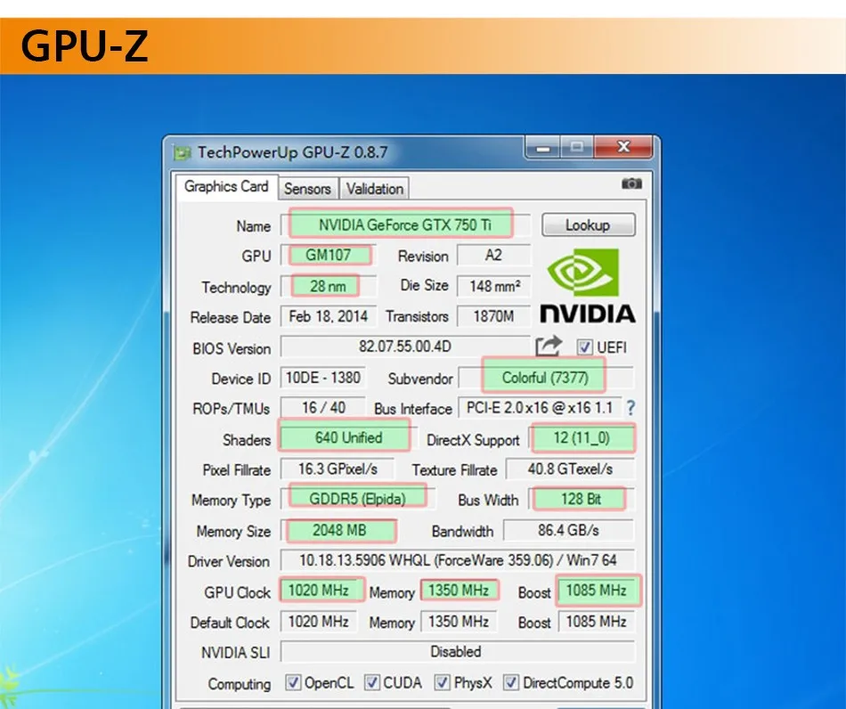
NVIDIA GeForce GTX 750 Ti Graphics Card
NVIDIA GeForce GTX 750 Ti Specifications
View full specs of NVIDIA GeForce GTX 750 Ti at VideoCardz.net
Card Status
Official
Manufacturer
NVIDIA
Release Date
18th February, 2014
Launch Price
$149 USD
Board Model
NVIDIA P2010
GPU
28nm GM107-400
Cores : TMUs : ROPs
640 : 40 : 16
Base Clock
1020 MHz
Boost Clock
1085 MHz
Effective Memory Clock
5400 Mbps
Max Computing Pwr (FP32)
1.39 TFLOPS
Memory Size
2048 MB GDDR5
Memory Bus Width
128-bit
Memory Bandwidth
86.4 GB/s
Interface
PCI-Express 3.0 x16
Thermal Design Power
60 W
News
2014-08-06 10:51
Galaxy to launch GeForce GTX 750 Ti HOF
News
2014-07-15 13:29
ASUS preps GeForce GTX 750 Ti STRIX
News
2014-06-04 08:09
Galaxy shows off GeForce GTX 750 Ti with DarbeeVision chip
News
2014-06-04 06:50
ASUS announces GeForce GTX 750 Ti STRIX Edition
News
2014-05-15 15:19
GeForce Black Edition just got smaller, thanks to Gigabyte
News
2014-03-31 19:21
Leadtek introduces GTX 750 Ti OC and GTX 750 OC
News
2014-03-11 20:00
Gigabyte to launch second factory-overclocked GeForce GTX 750 TI
News
2014-02-19 09:17
ZOTAC launches GeForce GTX 750 series with completely new design in China
News
2014-02-18 13:21
ZOTAC launches GTX 750 series and TITAN BLACK
News
2014-02-17 09:21
Galaxy GeForce GTX 750 Ti exposed, can be overclocked to 1.
35 GHz
News
2014-02-16 22:21
Colorful GeForce GTX 750 series detailed
News
2014-02-16 12:18
NVIDIA GeForce GTX 750 (Ti), official specifications and performance
News
2014-02-14 21:13
NVIDIA GeForce GTX 750 Ti and GTX 750 final specifications
News
2014-02-12 19:14
Exclusive: NVIDIA Maxwell GM107 architecture unveiled
News
2014-02-12 15:58
ASUS GeForce GTX 750 series detailed, plus the real specs of GM107!
News
2014-02-10 21:05
MSI GeForce GTX 750 (Ti) Maxwell Series detailed
News
2014-02-10 21:02
Gigabyte GeForce GTX 750 Ti and GTX 750 pictured and detailed
News
2014-02-05 20:43
NVIDIA Maxwell GM107 GPU pictured and detailed
News
2014-02-05 09:45
NVIDIA GeForce GTX 750 and GTX 750 Ti preview leaks out
News
2014-01-29 19:18
NVIDIA GeForce GTX 750 detailed
News
2014-01-27 11:33
TechPowerUP GPU-Z 0.
 7.6 adds support for GeForce GTX TITAN BLACK and GTX 750 (TI) series
News
2014-01-24 15:55
NVIDIA GeForce GTX 750 Ti specifications and benchmarks leaked
News
2014-01-21 07:36
ASUS GeForce GTX 750 Ti listed, coming mid-February?
News
2014-01-19 11:52
NVIDIA GeForce GTX 750 TI is 15% slower than GTX 660?
News
2014-01-16 13:36
NVIDIA GeForce GTX 750 Ti with Maxwell GPU in February
News
2013-10-03 09:59
NVIDIA GeForce GTX 750 Ti pictured and detailed
News
2013-09-09 10:11
NVIDIA To Launch GeForce GTX 750 Ti
News
2011-12-17 14:03
No NVIDIA 600 Series? Leaked GTX 780 (Kepler) Benchmark
NVIDIA GeForce GTX 750 Ti and GTX 750 Previewed
NVIDIA’s upcoming Maxwell based GeForce GTX 750 Ti and GeForce GTX 750 have been leaked and previewed by custom PC site, UKGamingComputers (via Videocardz). The surprising thing is that this is the second leak regarding the cards that is from a PC builder since the Chinese leak we saw earlier was also a custom gaming PC listing which included the GeForce GTX 750.
As expected, Maxwell is headed to consumers soon and will bring new levels of power efficiency, something that NVIDIA has strive to deliver with their Kepler generation of graphics processing units. Maxwell will have approximately three Tiers basically, Tier One will consist of 200W+ Discrete GPUs. The lowest tier will have 2W and 3W SoC Tegra Parts and ultra low voltage gpus. The middle tier will cover everything in between. The first GPU will ofcourse be the GM107 and will come in both Desktop and Mobile parts. The GeForce 800M lineup got announced a while back so it will be interesting to see some entry-level chips featuring the new core. The specs for both cards are detailed below:
NVIDIA GeForce GTX 750 Ti
The NVIDIA GeForce GTX 750 Ti will be the top most GM107 graphics card featuring 640 CUDA Cores, 40 TMUs, 16 ROPs and a 2 GB GDDR5 memory operating along a 128-bit interface. The clock speeds would be maintained at 1085 MHz for core, 1163 MHz boost and 1375 MHz memory clock though these might not be the reference clocks since we have noticed a lower clocked variant of the GeForce GTX 750 Ti in the past. The GeForce GTX 750 Ti would launch on 18th February 2014 for a price around $129-$139 US.
NVIDIA GeForce GTX 750
The NVIDIA GeForce GTX 750 (Non-Ti) is also based on the GM107 core architecture featuring 512 CUDA Cores, 32 TMUs, 16 ROPs and a 1 GB GDDR5 memory interface. The clock speeds for this graphics card are configured at the same 1085 MHz core and 1163 MHz boost but the memory runs slower at 5.1 GHz effective clock speed (1275 MHz QDR). Its safe to assume that these are factory overclocked models since we have already seen the previously listed GTX 750 with lower clock speeds of 1020 MHz core. The GeForce GTX 750 is also planned for launch on 18th February and would stick close to the $100 US price range.
NVIDIA GeForce GTX 750 and GeForce GTX 750 Ti Specifications:
| NVIDIA GeForce GTX 750 Ti | NVIDIA GeForce GTX 650 Ti | NVIDIA GeForce GTX 750 | NVIDIA GeForce GTX 650 | |
| GPU Codename | Maxwell GM107-400 | Kepler GK106 | Maxwell GM107-300 | Kepler GK107 |
| GPU Process | 28nm 148mm2 |
28nm 221mm2 |
28nm 148mm2 |
28nm 118mm2 |
| Cores | 640 | 768 | 512 | 384 |
| Core Clock | 1085 MHz | 928 MHz | 1085 MHz | 1058 MHz |
| Boost Clock | 1163 MHz | — | 1163 MHz | — |
| Memory | 2 GB GDDR5 | 1 GB GDDR5 | 1-2 GB GDDR5 | 1 GB GDDR5 |
| Memory Clock | 5400 MHz | 5400 MHz | 5100 MHz | 5000 MHz |
| Launch | February 2014 | 2013 | February 2014 | 2013 |
| Launch Price | $129 -$139 US? | $149 US | $119 US? | $119 US |
*Note — The clock speeds are not confirmed since these are factory overclocked variants.
Update — Videocardz has managed to get die shots of the Maxwell GM107 GPUs. The GeForce GTX 750 Ti is based on the GM107-400 core while the GeForce GTX 750 is based on the GM107-300 core. The GM107 measure exact 156mm2 and the power consumption for the GeForce GTX 750 Ti is rated at around 75W.
Previous and latest performance numbers leaked show the GeForce GTX 750 Ti rushing past the Radeon R7 260X and the GeForce GTX 750 competing against the Radeon R7 260. As i had already stated, NVIDIA could stir up some competition in this already heated sub-$150 market with these new arrivals. Their GeForce GTX 650 Ti boost is a well competitor and the Radeon R7 260X doesn’t show a good value against the Radeon HD 7850 2 GB models. AMD might answer with a price drop on their GPUs once the Maxwell GPUs are out. The GeForce GTX 750 Ti is confirmed to launch on 18th February, the GeForce GTX 750 is also expected to launch around the same date.
The numbers for UKGamingComputers show the GeForce GTX 750 faster than its predecessor, the GTX 650 and the GeForce GTX 750 Ti faster than the GeForce GTX 650 Ti.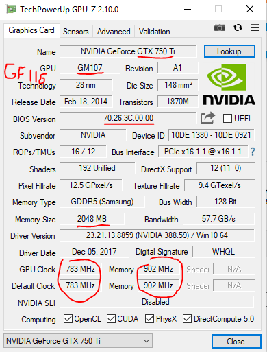 Comparison with GeForce GTX 660 was pointless since the card is set in a totally different price category. AMD is preparing their Radeon R7 250X as a response to the Maxwell cards but the specifications for that part are an unknown at the moment.
Share this story
GeForce GTX 750 Ti
Review NVIDIA today introduced the GeForce GTX 750 Ti and GeForce GTX 750 , which are the first carriers of the updated Maxwell graphics architecture. An important task in the development of new solutions was a fundamental improvement in the energy efficiency of devices. As a result, we have entry-level gaming graphics cards with a TDP of 60W, which do not require additional power, and only a 300W PSU is enough to run the system. Let’s figure out how the developers managed to achieve such a result. 92 calculators. At the same time, one control unit is used for such a numerous array of cores. Developing solutions for completely different categories of devices, ranging from computers for supercomputers to SoCs for tablets and smartphones, the company’s engineers gained certain knowledge to further improve the energy efficiency of the devices being developed.
The new first-generation Maxwell architecture uses the same functional APIs as Kepler, but involves a major redesign of the streaming multiprocessor internals. Now each SMM includes 4 independent computing units with 32 cores, which have their own instruction buffer and scheduler. Each such block also has 8 modules for loading and storing data (LD / ST), and the same number of nodes for performing special functions (Special Function Units, SFU). All structural modules have been redesigned, the control logic has been improved, and load balancing has been improved. The increased discreteness of modules allows more flexible and efficient use of GPU resources. Significantly increased the amount of cache memory in the second level. If the GK107 chips had a L2 capacity of 256 KB, then the GM107 received 2 MB of cache, which is even more than the top GK110 chip (1536 KB). Increasing the buffer allows you to partially reduce the impact of memory bandwidth and reduce the number of accesses to local RAM, thereby reducing the power consumption of the adapter.
According to the company, various changes have increased the performance of computing cores by 35%. Staying within the same process technology (28nm), NVIDIA managed to almost double the performance per watt of energy expended, as well as improve the performance per diem area ratio.
One of Kepler’s key innovations was the introduction of a hardware block for encoding/decoding H.264 video — NVENC. Using this module, these operations were performed much faster than using CUDA calculations, besides, these operations consumed noticeably less energy.
It was thanks to the advent of NVENC that the developers managed to implement the GeForce ShadowPlay technology, which allows recording a 1080p video stream in real time during the game with virtually no performance loss. It is also possible to organize the broadcast of video on Twitch. Note that in the latest version of GeForce Experience, it became possible to adjust the resolution of the video stream, change the frame rate (30 and 60), as well as the bit rate (10-50 Mb / s).
Within Maxwell, the NVENC block has been improved. If solutions based on Kepler could encode video at a speed of about 4 times faster than real time, then adapters based on Maxwell could encode video at 6–8 times faster. Video decoding capabilities have also been improved.
During video playback, Maxwell GPUs may enter the new GC5 mode. In this state, some units go into sleep mode without requiring additional power.
NVIDIA emphasizes that the presented solutions have the first generation Maxwell architecture, which is optimized for energy efficient solutions. Enthusiast devices will be based on second generation (2.0) Maxwell chips, but will be available at a later date. Obviously, the manufacturer’s desire to use graphics processors for top-end adapters made using a 20-nanometer process technology. Because these devices still have to wait.
GeForce GTX 750 Ti and GeForce GTX 750
The GeForce GTX 750 Ti and GeForce GTX 750 are the first graphics cards to feature NVIDIA Maxwell architecture graphics chips. Both are based on 28nm GM107 GPUs. The area of the crystal is 148 mm2, on which 1.87 billion transistors are placed.
The GeForce GTX 750 Ti uses the full weight version of the GM107. One computing cluster (GPC) in this case includes 5 SMM streaming multiprocessors, while the total number of CUDA computers is 640. The chip has 40 texture units and 16 rasterization modules. The base frequency of the GPU is set at 1020 MHz, while the average dynamic acceleration thanks to GPU Boost 2.0 is 1085 MHz.
GeForce GTX 750 Ti will often be offered with 2GB of GDDR5 memory, but 1GB RAM options are also acceptable. The nominal memory frequency is 5400 MHz. It is connected to the GPU via a 128-bit bus (2 × 64 bits), so the memory-GPU bandwidth is 86.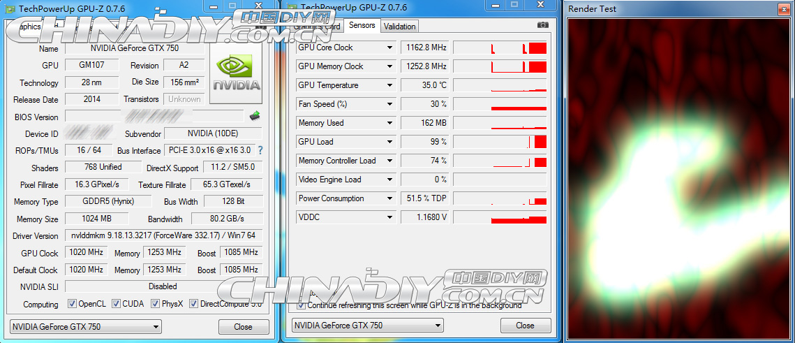 4 GB.
4 GB.
The reference adapter is very compact. The length of the PCB is only about 145mm. To cool the GPU, a cooler of very modest size and design is used. A small aluminum radiator is blown by a 60 mm axial fan.
The board layout is very simple. The power subsystem is made according to a 3-phase scheme (2+1). Four memory chips are placed in an L-shaped fashion next to the GPU. There is a place on the PCB for connecting a 6-pin connector, but the connector itself is not soldered. Given the declared TDP level of 60 W, the capabilities of the PCI Express x16 slot (75 W) will be enough for the full operation of the video card. For a system with a GeForce GTX 750 Ti, the manufacturer recommends using a PSU with a power of 300 W or more.
The interface panel of the reference model has three video outputs — a pair of DVI (DVI-D and DVI-I), as well as mini-HDMI. Despite the single-slot mounting plate, the video card will require two slots to install in the system.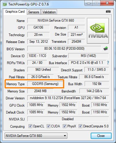
The GeForce GTX 750 uses a similar hardware platform, with the only difference that the GM107 GPU in this variant has 4 streaming multiprocessors. Accordingly, the number of processing cores has been reduced from 640 to 512, the number of texture units has been reduced to 32, the number of rasterizers has remained at the same level — 16. Frequency formula GM107 uses the same frequency formula as 1020/1085 MHz. The memory also runs at 5400 MHz and is connected to the chip via a 128-bit bus. The GeForce GTX 750 has a TDP of 55W.
Video card manufacturers have introduced original versions of adapters. In terms of layout and cooling systems, NVIDIA does not limit developers. As expected, with the announcement of the first solutions at Maxwell, variants with significantly increased clock frequencies, completely redesigned printed circuit boards, and exclusive cooling systems are presented. Moreover, some manufacturers offer GTX 750 Ti models equipped with additional power connectors. Such modifications should work well during overclocking.
Positioning
As for the positioning of new video cards, the GeForce GTX 750 Ti and GeForce GTX 750 models occupy the GeForce GTX 650 Ti niche in the current line of NVIDIA solutions. At the same time, the GTX 650 is still in service. The position above the GTX 750 Ti is occupied by the GeForce GTX 660. On the presented graph, there was no place for the GeForce GTX 650 Ti BOOST, which have now practically disappeared from sale. Probably, the GTX 750 Ti should partly insure this model as well.
NVIDIA also offers to consider video cards based on Maxwell architecture as an upgrade for solutions from previous generations. In particular, the GeForce GTX 750 Ti could be a replacement for the GeForce GTX 550 Ti. Despite the fact that the latter was introduced in early 2011, according to Steam statistics, it is still among the top five most popular video cards among active users of this service. The novelty should provide twice the number of frames / s, while the declared power consumption of the GTX 750 Ti is also almost 2 times lower (60 W vs.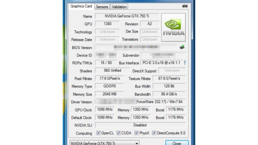 116 W). This means that the performance / watt ratio of a Maxwell GPU device is about 4 times higher than that of a device of the same class on Fermi.
Price
The recommended price for the GeForce GTX 750 Ti for the US market is $149 (excluding tax) for the 2 GB version. Model GeForce GTX 750 is estimated by the manufacturer at $119. In Ukraine, the expected prices are between UAH 1290 and UAH 1090, respectively. Recall that a few days ago, AMD presented its solutions in this price category. Thus, the Radeon R7 265, which is actually an analogue of the Radeon HD 7850, will be offered for the same $149, while the price of the Radeon R7 260X has been reduced from $139.up to $119. Against the background of the current cost of the Radeon line, such information looks very optimistic, for conclusions it is necessary to wait for devices to appear in retail at this price.
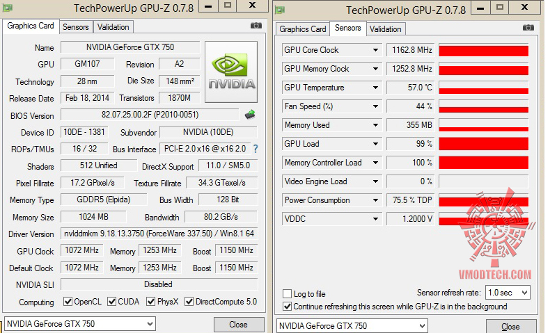
GeForce GTX 750 Ti Express Test
We’ve done a quick test of the GeForce GTX 750 Ti reference model and are ready to share the first results.
Note that under load the temperature of the GM107 processor increased to 65 C. Despite the dimensions, the fan noise level was minimal. In games, the clock frequency of the chip, thanks to GPU Boost 2.0, increased automatically to 1150 MHz. Given that the temperature of the chip was at an acceptable level, its frequency did not actually decrease.
For the initial evaluation of the performance of the new NVIDIA solution, we included the GeForce GTX 650 Ti, as well as classmates from AMD — the Radeon R7 260X and R7 260. At the time of the tests, we had adapters with only 1 GB of memory. Obviously, 2-gigabyte versions would show great results in some cases, but would not fundamentally change the overall picture.
The first tests show that the performance of the GeForce GTX 750 Ti in some cases is 20-30% higher than that of the GTX 650 Ti. In some cases, the results are more modest (12%), while in real games the advantage can reach an impressive 36% (Bioshock Infinite).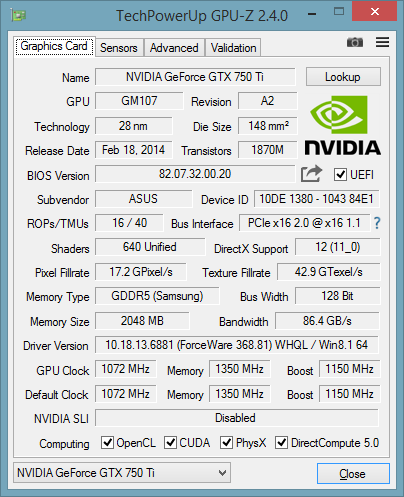 Note that the GeForce GTX 650 Ti TDP is 110W, while the GTX 750 Ti is 60W. Comparing the performance results, one can only wonder how NVIDIA managed to improve the power efficiency of its solutions so dramatically.
Insufficient data available for comparison with competing AMD devices. We can only state that the GeForce GTX 750 Ti is noticeably more productive than the Radeon R7 260X, but for a more detailed assessment, additional tests are needed, which we will conduct in the near future. We will also take a closer look at the actual power consumption and overclocking capabilities of new devices equipped with Maxwell architecture GPUs.
UPD. 02/26/2014 — GeForce GTX 750 Ti: overclocking, performance and power consumption
Why is Nvidia GeForce GTX 750 better than Nvidia GeForce GTX 750 Ti?
- 5W below TDP?
55W vs 60W
Why is Nvidia GeForce GTX 750 Ti better than Nvidia GeForce GTX 750?
- 0.
 26 TFLOPS above FLOPS?
1.31 TFLOPS vs 1.04 TFLOPS - 100MHz faster memory speed?
1350MHz vs 1250MHz - 1GB more VRAM?
2GB vs 1GB - 400MHz higher effective clock frequency?
5400MHz vs 5000MHz - 8.2 GTexels/s higher number of textured pixels? more memory bandwidth?
86.4GB/s vs 80GB/s - 128 more stream processors?
640 vs 512 - 8 more texture units (TMUs)?
40 vs 32
Which comparisons are the most popular?
Nvidia GeForce GTX 750
vs
Nvidia GeForce GT 1030 DDR4
Nvidia GeForce GTX 750 Ti
vs
AMD Radeon RX 550
Nvidia GeForce GTX 750
vs
Nvidia GeForce GTX 1050
Nvidia GeForce GTX 750 Ti
vs
MSI Radeon RX 580
Nvidia GeForce GTX 750
vs
Nvidia GeForce GTX 1060
Nvidia GeForce GTX 750 Ti
vs
Nvidia GeForce GT 1030 DDR4
Nvidia GeForce GTX 750
vs
AMD Radeon RX Vega 8
Nvidia GeForce GTX 750 Ti
vs
Nvidia GeForce GTX 1650
NVIDIA GEFORCE GTX 7500003
vs
Nvidia GeForce GTX 550 Ti
Nvidia GeForce GTX 750 Ti
vs
AMD Radeon RX 580
Nvidia GeForce GTX 750
vs
AMD Radeon RX 560
Nvidia GeForce GTX 750 Ti
vs
NVIDIA GeForce GTX 960
NVIDIA GEFORCE GTX 7500003
10. 0 /10
0 /10
2 reviews of users
Functions
Price and quality ratio
10.0 /10
1 votes
10.0 /10 9000
2 Votes
933 /10
1 Votes
8.5 /10
2 Votes
performance
/10
1 Votes
7.5 /10
2 Votes
Sundance of work
6.0 /10
1 Votes
5.5 /10
2 Votes
Reliability
4444 /10 9000 9000 9000 1 VOTES
.0.00
2 votes
Performance
GPU clock speed
1020MHz
1020MHz
The graphics processing unit (GPU) has a higher clock speed.
Turbo GPU
1085MHz
1085MHz
When the GPU is running below its limits, it can jump to a higher clock speed to increase performance.
pixel rate
16. 3 GPixel/s
16.3 GPixel/s
The number of pixels that can be displayed on the screen every second.
FLOPS
1.04 TFLOPS
1.31 TFLOPS
FLOPS is a measure of GPU processing power.
texture size
32.6 GTexels/s
40.8 GTexels/s
Number of textured pixels that can be displayed on the screen every second.
GPU memory speed
1250MHz
1350MHz
Memory speed is one aspect that determines memory bandwidth.
Shading patterns
Shading units (or stream processors) are small processors in a graphics card that are responsible for processing various aspects of an image.
texture units (TMUs)
TMUs take texture units and map them to the geometric layout of the 3D scene. More TMUs generally means texture information is processed faster.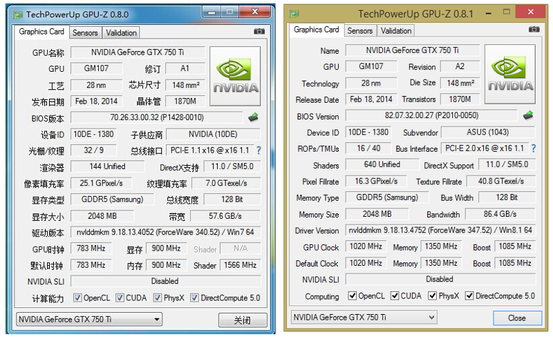
ROPs
ROPs are responsible for some of the final steps of the rendering process, such as writing the final pixel data to memory and for performing other tasks such as anti-aliasing to improve the appearance of graphics.
Memory
effective memory speed
5000MHz
5400MHz
The effective memory clock is calculated from the size and data transfer rate of the memory. A higher clock speed can give better performance in games and other applications.
maximum memory bandwidth
80GB/s
86.4GB/s
This is the maximum rate at which data can be read from or stored in memory.
VRAM (video RAM) is the dedicated memory of the graphics card. More VRAM usually allows you to run games at higher settings, especially for things like texture resolution.
memory bus width
128bit
128bit
A wider memory bus means it can carry more data per cycle.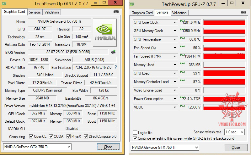 This is an important factor in memory performance, and therefore the overall performance of the graphics card.
GDDR memory version
Later versions of GDDR memory offer improvements such as higher data transfer rates, which improve performance.
Supports memory troubleshooting code
✖Nvidia GeForce GTX 750
✖Nvidia GeForce GTX 750 Ti
Memory troubleshooting code can detect and repair data corruption. It is used when necessary to avoid distortion, such as in scientific computing or when starting a server.
Functions
DirectX version
DirectX is used in games with a new version that supports better graphics.
OpenGL version
The newer the OpenGL version, the better graphics quality in games.
version of OpenCL
Some applications use OpenCL to use the power of the graphics processing unit (GPU) for non-graphical computing. Newer versions are more functional and better quality.
Supports multi-monitor technology
✔Nvidia GeForce GTX 750
✔Nvidia GeForce GTX 750 Ti
The video card has the ability to connect multiple screens. This allows you to set up multiple monitors at the same time to create a more immersive gaming experience, such as a wider field of view.
GPU boot temperature
Unknown. Help us offer a price. (Nvidia GeForce GTX 750)
Lower boot temperature means the card generates less heat and the cooling system works better.
supports ray tracing
✖Nvidia GeForce GTX 750
✖Nvidia GeForce GTX 750 Ti
Ray tracing is an advanced light rendering technique that provides more realistic lighting, shadows and reflections in games.
Supports 3D
✔Nvidia GeForce GTX 750
✔Nvidia GeForce GTX 750 Ti
Allows you to view in 3D (if you have a 3D screen and glasses).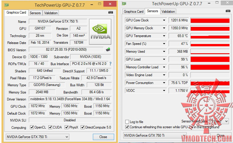
supports DLSS
✖Nvidia GeForce GTX 750
✖Nvidia GeForce GTX 750 Ti
DLSS (Deep Learning Super Sampling) is an AI based scaling technology. This allows the graphics card to render games at lower resolutions and upscale them to higher resolutions with near-native visual quality and improved performance. DLSS is only available in some games.
PassMark (G3D) result
Unknown. Help us offer a price. (Nvidia GeForce GTX 750)
This test measures the graphics performance of a graphics card. Source: Pass Mark.
Ports
has HDMI output
✔Nvidia GeForce GTX 750
✔Nvidia GeForce GTX 750 Ti
Devices with HDMI or mini HDMI ports can stream HD video and audio to an attached display.
HDMI connectors
Unknown. Help us offer a price. (Nvidia GeForce GTX 750)
More HDMI connectors allow you to connect multiple devices such as game consoles and TVs at the same time.