An easy to build MCS-48 (8748 / 8749 / 8741 / 8742 / 8048 / 8049 / 8050 / 8755) Programmer / Reader – Matt’s Tech Pages
Recently I was repairing an old piece of equipment which was based on Intel’s first microcontroller: The MCS-48.
The nice thing about the MCS-48 is that it largely predates the concept of code security. With the exception of some newer dated parts, usually 8042 / 8049, if you’ve got the thing, you can steal the code from it, disassemble it, and learn lots about the equipment it’s fitted to.
In the past I have built a series of Arduino shields for programming old UV erasable devices for which programming hardware is difficult to come by (read more here). This is not so much the case for MCS-48 as hardware can be obtained for a hundred dollars or so, however, I wasn’t going to pass up on the opportunity to build another one of these, and, mine can be built for less money plus it has the ability to read mask ROMs.
At the same time as I designed the shield, I also built an entirely new project based on one of these. More about that here.
Programming and reading the list of devices mentioned in the title requires quite a range of different voltages including 5V, 12V, 18V, 21V, 23V and 25V. This programmer can generate all of them and software select between them as needed.
Supported devices
Regular UV erasable MCS-48
Parts 8748 and 8749. Vpp = 21V.
These were made also made under license by NEC. This programmer supports both NEC and Intel parts.
UV erasable UPI-41/42
Parts 8741 and 8742. Vpp = 21V for 8742. Vpp = 25V for 8741.
As with above, NEC parts also supported.
Mask ROM MCS-48
Read code only. Parts 8048, 8049 and 8050. EA = 12V. Note that not all MCS-48 mask ROM parts will allow the code to be read out.
8755A
An adapter is required to program the 8755A. There is a little bit of backstory about it here.
Build resources are linked to at the end of the page.
Warning to those building other designs
All home-brew MCS-48 programmers have pin drivers resembling the above, mine differs in that it uses a P-Ch FET and a 2K2 “pull-down” is also present to keep fall times within specification (< 2μS).
This is particularly important when programming CMOS parts, otherwise the timings specified in Intel datasheets cannot be achieved, instead arbitrary delays would have to be inserted throughout the programming algorithm to allow charge to bleed away from these inputs, as is frequently seen in other efforts.
The most important difference however, is the 220Ω resistor. Some batches (particularly 8742’s and some 8749’s) are very sensitive to over-current on the PROG pin. I purchased about 50 MCS-48 samples when designing my programmer, and blew a quarter of them discovering this.
This value was chosen because it reliably programs the earliest 1K NMOS parts, which require more current on this pin, and don’t appear to have this problem, while not destroying sensitive 2K parts.
Host software / firmware
Please see the main project page for more information.
Schematic
- Can be downloaded from here.
Gerbers
There are two versions of the gerbers. A “Long” version which has the exact dimensions of an Arduino Mega. Choose this if your PCB house doesn’t charge extra for exceeding 100x100mm dimensions. Total size is 101.5mm x 53.5mm.
The “Short” version has the tab at the end clipped to keep it under 100mm. Total size is 99.95mm x 53.5mm.
- “Long” gerber download
- “Short” gerber download
BOM
Can be downloaded from here (or here – CSV).
8755A Adapter
- Download schematic
- Download gerbers (PCB size is 67.31mm x 45.08mm)
The 8755A adapter only has 3 parts:
- 0.1uF (or whatever) bypass capacitor.
- Samtec APA-640-T-A 40 position IC plug. These are a little difficult to come by. Instead have a search around for “male IC pins” there are various snap off types available. I wouldn’t recommend using regular 2.54″ pin headers as they’ll potentially damage the socket in the base unit.
- 3M 240-3346 40 pin IC socket (anything roughly this form factor will do).
The Intel 8048 and 8748 – EEJournal
Intel announced the first commercially successful microprocessor, the 4004, in late 1971. By 1974 Intel had introduced four microprocessors: the 4-bit, “low-end” 4004 and the upgraded 4040, and the 8-bit 8008 and 8080. Intel’s 4-bit 4004 and 4040 microprocessors were used primarily for embedded control applications where I/O capabilities and performance and lower part cost outweighed the superior processing performance of 8-bit devices. However, Intel no longer had the microprocessor market to itself. Several other semiconductor vendors had introduced competing microprocessors by 1974, notably the 4-bit Rockwell PPS4, the 8-bit Motorola 6800, the multichip Fairchild F8, and National Semiconductor’s 16-bit, multichip IMP-16. Toshiba had designed, built, and delivered the 12-bit TLCS-12 microprocessor specifically as an engine controller for Ford, and many more microprocessors were on the way.
Even worse, the 4-bit TMS1000 microcontroller family, introduced by Texas Instruments (TI) in 1974, put a 4-bit CPU, RAM, ROM, and I/O circuitry on one chip, which simplified system design and cut the cost of processor-based control significantly. The introduction of TI’s TMS1000 family certainly got the attention of several prospective customers (and several semiconductor makers). Intel, under siege, was starting to lose embedded system designs to microprocessor and microcontroller competitors in the embedded market. That had to stop. Intel needed to respond, and the company knew it.
When Henry Blume Jr. arrived at Intel in October 1974, there was already an internal agreement that the company would develop a microcontroller. Intel was already making microprocessors, RAM chips, ROMs, and UV-erasable EPROMs and had the process technologies to make these parts in house. The main decision yet to be made was whether the microcontroller would have a 4-bit CPU, like the TMS1000, or an 8-bit CPU. According to an oral history panel conducted by the Computer History Museum (CHM) in 2008 with many of the people responsible for developing the 8048, Ed Gelbach, Intel’s Senior Vice President of Corporate Marketing, made the decision. Intel’s microcontroller would have an 8-bit CPU because a 4-bit CPU didn’t have enough sex appeal. (Note: The 8048 oral history in the reference section contains several references to sex appeal, not in a sexual context, which seems to have been used as a frequent figure of merit at Intel during those times.)
Although the 8048 is the generic name that’s traditionally used for Intel’s first microcontroller – the actual family name is MCS-48 – the oral history makes it clear that the 8748 EPROM version appeared first. That’s because the 8748 could be used immediately for software development and early prototyping and it would take a year or two for customers to develop their software to the point where they could order ROM-based 8048 devices. The 8748 would also be a more difficult device to manufacture because Intel’s EPROM process technology was quite different from the company’s other process technologies, so it made sense to have that device ready first, and then take the next year to design the ROM-based 8048. Finally, Intel could and would charge a lot more money for a reusable 8748, which meant the company could collect more revenue, sooner.
David Stamm joined Intel in January 1974, and initially worked on fixing bugs with the 4004 and 4040 microprocessors, which were in production at the time. He then designed the Intel 4308, a support chip for the Intel 4040 that combined a 1-Kbyte ROM with some I/O ports. The 4308 combined the functions of four Intel 4001 chips that combined a 256-bit ROM with an I/O port, so the 4308 contained about half a microcontroller, lacking a CPU and RAM. After designing the 4308, Stamm was assigned to the 8048 project. He states in the 8048 oral history that he was single at the time and so he “lived and breathed the 8048 for two-plus years, night and day.”
Stamm’s first responsibility was to develop the microcontroller’s instruction set. It would be all new, to suit an 8-bit microcontroller instead of the microprocessors that Intel was already making. In the oral history, Stamm recalls:
“There were three of us who were full-time on the project: myself, I was in charge of the instruction set and the logic design and the overall chip schedule; David Buddy, who was in charge of the complex tasks associated with integrating the EPROM technology and all of the EPROM programming logic and the sensing logic for the EPROM components, as well as most of the circuit design; and then Dwayne Hook who was responsible for all of the layout of the chip…
“The first phase was really the instruction set design. So here I am, I’m out of college a year, had a Bachelor’s degree, thinking to myself what business do I have developing the next generation instruction set for these components? And really, nobody was looking that carefully over my shoulder, but I said, okay, fine I’ll go for it. Luckily, in college I had taken assembly language programming in a language called COMPASS, which was part of CDC, which is no more.
“But I learned a lot about assembly language programming there, and then I’d worked on the 4040 and I looked at all the other instruction sets in order to try to come up with what kind of instruction set might make sense. The challenge was [that] you had to consider the instruction set in terms of how much complexity in die-cost it would be.
“So, for example, subtractions and compares would be really valuable instructions, but they added dramatically in additional chip area. So, I decided we really couldn’t afford those, especially since we were going to go into an 8-bit design. I had been a big proponent of 8-bit. One of the counter arguments was cost and die-size. So, during these design steps I did everything I could to jettison features and functions that I thought was going to add extra die-size. Looking back at it now, I think I probably went a bit overboard — although at the time it would’ve been difficult to have made that conclusion.”
At one point in the oral history, Blume interjects:
“I also want to point out Dave’s two famous – or his favorite instructions were SEX and SIN, which stood for set external mode and set internal mode. And then when the people in systems took over, they removed SEX and SIN… they renamed them.”
Limitations in the 8048’s design, made to ensure that the chip could be manufactured with the available process technology, were not restricted to the instruction set. Memory-space limitations were another important restriction. The original 8048 had a 4-Kbyte address space limit for program memory, but it was really split into two 2-Kbyte banks. The 8048’s program counter ostensibly had 12 bits, but the most significant bit came from a separate register that could be used for bank switching. Initially, the 8048 incorporated a 1-Kbyte program memory, so this decision didn’t pinch at first. Eventually, it would. Stamm explains, “…there were lots and lots of limitations that existed, primarily in order to keep the die-size down.”
Intel had no simulation software in those early days, so the design team built a breadboard instead. Stamm recalls:
“So, we built this large breadboard, which in and of itself was yet a whole other design project, using the same type of combinatorial logic that we were hoping to eliminate through the development of the 8048… we were using TTL and DTL devices, and the breadboard was huge as I recall. It was probably five foot tall by two or three feet wide, just completely covered with wiring on the back.”
Such was the state of the art for chip design in those days.
Before releasing the new microcontroller to production, the design team had to meet with the Intel executives – Andy Grove, Gordon Moore, and Lex Vadasz – and convince them that the 8748 was ready to enter the market. A demo was in order, and Stamm decided to write a blackjack program. Stamm loved to gamble and frequented Lake Tahoe casinos. The programmed 8748 would drive a dumb terminal, presumably through an RS-232 voltage translator. Stamm recalls that he discovered the limitations of his own microcontroller instruction set while writing the blackjack program. He also filled the 8748’s program memory and did not have room to add a double-down feature to the blackjack game. The very first application program written for the 8048 immediately brought its main limitations to light.
To add sex appeal to the demo, the team decided to power the 8748 with a battery made from strips of copper and zinc stuck into a lemon or an orange. At least that’s how it’s described in the oral history. The 8748 needs 5 volts at 100 milliamps to run, and a copper-zinc battery made from one orange generates a volt or less, so either more than one orange was used to power this demo or the story is apocryphal. It’s a great story though.
Intel announced the MCS-48 microcontroller family, which included the 8048 and 8748, in late 1976, with the goal of shipping 1000 revenue units, all 8748 devices, in the first quarter of 1977. Blume recalls that the actual number of revenue units shipped was 770, which everyone considered a success and is no doubt the result of a lot of pre-selling. The Intel 8748 was a hit. Product manager Howard Raphael recalls early customers including Gilbarco (gasoline pumps), Tektronix, and Chrysler.
Magnavox based its Odyssey2 video game console on an 8048. The 8048 was used extensively to power a variety of analog music synthesizer keyboards including the Korg Trident series, the Korg Poly-61, the Roland Jupiter-4, and the Roland ProMars.
Like many analog music synthesizers, the Roland Jupiter-4 used an Intel 8048 as a controller. Image credit: Raymangold22, Wikimedia Commons
The Sinclair QL personal computer used an Intel 8049 (an 8048 with a 2-Kbyte ROM) to manage its keyboard, joystick ports, RS-232 inputs, and audio output.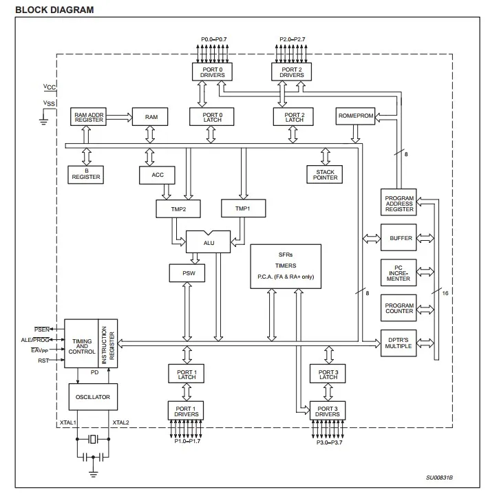 Nintendo used the ROM-less 8035 microcontroller (quite possibly an 8748 with a bad EPROM) in its original Donkey Kong arcade game to generate the game’s music. My friend and colleague Wally Wahlen incorporated an Intel 8048 as a controller into his design of the Hewlett-Packard 9876 thermal page printer, which was introduced in 1979.
Nintendo used an 8035 (a ROM-less 8048) to generate music in its Donkey Kong video game arcade console. Image credit: Rob Boudon, New York City, USA, Wikimedia Commons
Eventually, the IBM PC would use an Intel 8048 as a keyboard controller. However, the IBM PC was not the first computer to use the 8048 this way. That milestone belongs to the Tandy TRS-80 Model II, which used a cost-reduced, 28-pin version of the 8048 called the 8021 to manage its detachable keyboard and scan the keys.
The Tandy Model II personal computer used an 8048 as a keyboard controller. Image credit: Piergiovanna Grossi, Wikimedia Commons
The Intel 8048 family became a huge success for Intel, but its design limitations surfaced almost immediately. The limitation on program address space began to noticeably pinch customers by 1977, and, by the fourth quarter of that year, just a year after its introduction, Intel started to define the 8048’s successor, which would be called the 8051. It would become an even bigger success and could easily be called the microcontroller that would not die, at least not yet. However, that story must wait its turn.
References
Oral History Panel on the Development and Promotion of the Intel 8048 Microcontroller, Computer History Museum, July 30, 2008
Retro-development for the first portable console from the distant 1979 / Sudo Null IT News
In 1974, Texas Instruments releases the first 4-bit microcontrollers of the TMS1000 family, and in 1976 Intel begins production of 8-bit microcontrollers of its famous MCS-48 series. And then it began.
Due to the cheapness and self-sufficiency of microcontrollers (then they were called directly — a single-chip microcomputer), consumer electronic devices have grown dramatically smarter, and their number has grown like never before. With the advent of microcontrollers, such a class of devices as portable electronic games arose, the scale of the “disaster” can be estimated at this link. Among all this variety of early games, one that stood out, which I will talk about in this post, is Milton Bradley Microvision, the first portable electronic game with replaceable cartridges that used both of the microcontrollers mentioned above. I will also try to elaborate on the specifics of development for this console.
General description
Microvision was released in the USA almost forty years ago, in 1979. In total, 12 cartridges with games were sold for it, among which were the Block Buster (analogue of Breakout) that came with the console, sports games — Bowling and Baseball, an electronic version of the famous board game Connect Four, Pinball and others. Most of the games can be evaluated on the MVEM emulator, which was made on the basis of an interesting series of publications, from which I also learned a lot of useful things. Here I will not dwell on the description of the original games of the console, but will immediately move on to its inner world.
An important feature of the console is a 2-inch LCD display with a resolution of 16×16 pixels. Pretty primitive by today’s standards, but compared to the LED assemblies and vacuum fluorescent indicators used then in portable games, the dot-matrix LCD screen was a fairly progressive step. In addition to Microvision, in the same year, a series of Mego Mini-Vid electronic games with a similar screen, though 13×20, went on sale. Apparently, at that time, these were the only devices in wide sale with matrix LCDs of this resolution.
Display driven by Hughes chip SCUS0488 is a dot matrix LCD driver. The driver is powered by a negative voltage stabilizer UA79MG with a piping of a pair of capacitors and resistors — that’s the whole simple element base.
The body of the console also houses the controls — a 4×3 button matrix and a 10 kOhm variable resistor as a paddle. There is a piezo speaker for sound reproduction.
The most important reason why Microvision went down in history, and everyone forgot about the Mini-Vid mentioned above, is the use of replaceable cartridges.
Externally, the cartridge was a detachable upper part of the housing. In the center of the cartridge there was a plastic window covering the screen, on which colored game elements and inscriptions individual for each game were applied. Below were the holes for the buttons, covered at the back with a thin film on which the signatures were applied, and for each game, holes were made only for the buttons used. Probably, such a layout of the cartridge, as conceived by the authors, made it possible to maximally adapt the console to a specific game.
Block Buster game board, in the case and on the reverse side
The electronic part of the cartridge was built on one of two microcontrollers — TMS1100 or Intel 8021 with the necessary binding. Placing the «brain» of the console in a cartridge may seem like a bit of an odd decision, but it allowed for only two chips per game. In addition, it also added versatility. At the same time, the price of the cartridge, due to the presence of a microcontroller, apparently did not increase much (for example, the cost of 8021 in large lots of 1976 was about $3).
All this was fed by one or two crowns connected in parallel (8021 was rather voracious). Moreover, in later versions, the contacts for the second battery were removed, and the remaining space was recommended to be used for a spare battery. Apparently, this was due to the fact that users often confused the polarity, getting a rather dangerous short circuit.
Tie
I bought this ancient console with the aim of writing some game for it and making a cartridge, and copying the element base of the original as much as possible.
But there is one significant problem here — that TMS1100, that Intel 8021 had a masked ROM, i. e. programmed at the factory during the manufacturing process. There is a way out for the Intel microcontroller: 8021 is a stripped-down version of 8048, which also had a mask ROM, but Intel released an analogue of 8048 with a programmable ROM — 8748, both in the version with ultraviolet erasure and cheaper one-time programmable.
For the TMS1100, the situation, unfortunately, is much worse — there was a debug version of the chip that worked with an external ROM — TMS1098, but it is very difficult to buy it now, if possible. In addition, the microcircuit was made in a DIP-64 package, which itself is huge and will not fit into the cartridge in length, and a rather big ROM is also needed.
In general, UV-erasable 8748 is the way to go, and the final cartridge can be made on a non-erasable version.
Top one-time programmable P8748H and bottom UV-erase D8748H
Intel 8021
Below I will give a brief description of exactly 8021, and not 8748, because I will use only the truncated features of 8021 in order to have only the resources originally laid down by the console developers.
The memory subsystem, like the entire MCS-48 family, is based on a modified Harvard architecture. Program memory — internal ROM with a capacity of 1024 bytes, data memory — 64 bytes of dynamic RAM.
The organization of the RAM is shown in the following figure:
Cells 0-7 occupy directly addressable working registers R0-R7, and R0 and R1 can be used as pointers for indirect access to all RAM cells. Cells 8-23 are used for the 8-level call stack, although they can also be used via R0-R1.
The microcontroller has a built-in clock generator, the reference frequency is set by an external crystal, RC circuit or LC circuit. The machine cycle lasts 10 cycles, and each cycle takes 3 cycles of the reference frequency. The maximum frequency is 3.58 MHz, while the machine cycle lasts 8.38 µs. The minimum frequency is limited by the specifics of DRAM operation and is 600 kHz.
8021 contains two 8-bit ports and one 4-bit port, which can also be used to connect an I / O port expander, IC 8243. All ports are quasi-bidirectional.
In addition, the microcontroller has a built-in eight-digit timer/counter. In timer mode, counter T is incremented by 1 every 32 machine cycles. When T overflows, the TF flag is set. In the counter mode, the pulses received at the test input T1 are counted.
The instruction set contains 64 instructions, of which 36 are executed in one cycle, and 28 in two. Most instructions are single byte.
List of instructions with short descriptions
Preparation
There were no problems with the purchase of 8748, the main thing to pay attention to is that microcircuits were produced using different technologies. The earliest NMOPs required 25V for firmware and were labeled D8748. By the end of the 70s, these microcontrollers began to be built using HMOP-E technology (an improved version of NMOP from Intel), were marked D8748H and required 21V. The same voltage was required by a later clone from NEC (mPD8748H). The one time programmable version was marked P8748H.
The simplest and cheapest Chinese UV eraser was bought with a mechanical timer, which, as practice has shown, copes with its task perfectly (although the accuracy of the timer at short intervals is no). It reliably erases the ROM of microcircuits in ~ 2.5 minutes. Later, I bought a ZAX Quick-EII eraser for a symbolic price from Japanese hands, I don’t even know what year it is, it looks like the beginning of the 90s. It uses a xenon flash and erases 8748 in 3(!) seconds, literally. A video (not mine) with a demonstration of work can be viewed here.
The programmer turned out to be the main problem. Support for this outdated Intel family in modern programmers is available only at a cost of $ 300. Although, there is a relatively cheap amateur Willem, which can work with the MCS-48 through an adapter, but it needs an LPT, which did not suit me at all. I had to solder myself. I am, let’s say, a beginner radio amateur, so I spent about a week with him, killing one of the two 8748s that had arrived by that time (although I amuse myself with the thought that it was originally like that). I took the circuit published here as a basis, only adapted it for Atmega and a more convenient 24V power supply. All soldered on a breadboard:
It turned out, of course, rather clumsy, and one of the mosfets works at the limit (even a little beyond), but, in the end, the programmer did its job and served me well.
So, everything is ready, the test firmware flashes cheerfully with the LED, it’s time to make the cartridge.
Cartridge
The bulk of the cartridges worked on the TMS1100, because Signetics, which produced the 8021 under license from Intel, could not provide the required MB of chip shipments. Even some games that were already written for the 8021 had to be ported to the TMS1100. This, by the way, made it possible to abandon the dangerous bundle of two batteries, because the consumption of the microcontroller from TI was only 0. 1W versus 1W from Intel. Out of 6 cartridges, I have only one with 8021, this is the Connect Four game, and it was taken as a basis.
I tried to make the board as close to the original as possible, but of course I had to make changes. First, the chip size (DIP-40 vs DIP-28) and different pinouts. Secondly, I had to change the ratings in the oscillatory circuit that sets the clock frequency, because. the machine cycle for the HMOS versions of the chips is 15 cycles, and for the MOS versions that were used in the original cartridges, 30 cycles. Therefore, for complete authenticity, my cartridge will operate at 1.25 MHz against the original 2.5 MHz, while still providing the same performance.
In the photo above, finished printed circuit boards ordered in China, and while they were going, I drew and etched the board and assembled such a “debugging complex”:
Finally, the hardware part is ready and you can start programming.
Display
First of all, it was necessary to deal with the output to the LCD display. As I wrote above, it was controlled by the Hughes 0488 driver using multiplexing (an interesting article about this LCD control method was recently published on Habré). It is a driver, not a controller, so you can’t just turn on some pixel and go about your business, you need to constantly update the screen contents with a frequency of 30-50Hz with low-level commands.
Connection scheme is as follows:
Wiping H0488:
VDD -Power (3-8V)
R1-R16 -Line Control Departments
C1-C16 -Stage Management Expits
DATA0 DATA -DATA3 — Data bus
!Data Clk — Clock signal input for data recording
Latch Pulse — Signal for fixing the status of pins R0-R15, C0-C15
The meaning of the microcircuit is as follows:
Through 4 information lines, the required state of all 32 microcircuit outputs is sequentially set (16 per row and per column). Those. we indicate the state of the outputs in 4-bit chunks for rows 1-4, then 5-8, 9-12 and finally for 13-16, and also 4 times 4 bits we indicate the state of the columns. Each new piece of data is clocked by a pulse on the !DATA CLK line. After we have sent all 8 portions of data, we set the specified state of the outputs R1-R16, C1-C16 with an impulse along the Latch Pulse line, which will be held until the next impulse along this line.
Naturally, in one such cycle we cannot specify the state of each individual pixel independently of the others, we can only 16 (by the number of intersections of rows with columns). Therefore, to independently update the state of each pixel, it will take 256/16 = 16 cycles.
In addition, it is our responsibility to switch the polarity to eliminate the constant voltage of the LCD electrodes, otherwise the display will quickly degrade. Polarity switching occurs on the trailing edge of the Latch Pulse signal when the !Data Clock input is low. Polarity is recommended to be switched with screen refresh rate.
The above is illustrated by the following timing diagram from the datasheet:
All this, implemented in 8021 assembler (which, by the way, is significantly reduced compared to the assembler of the rest of the family, for the same authenticity I used only instructions supported by 8021), can look like this:
mov R0, #32 ;Pointer to image in RAM.mov r1, #10000000b ;Set bit position in r1-r2 mov r2, #00000000b ; defines the current line. mov r4, #00000010b ;We will pull the second bit !DATA CLK. mov r3, #11110000b clr c loop: ;Set the values of pins r1-r16 for the current line. mov a, r1 ;High nibble of register r1 loadNibble ;Set levels for pins R1-R4. mov a, r1 ; Take lower 4 bits of register r1 rrc a ; and shift to prepare it for the next iteration, xch a, r1 ;and use the current content now. swap a loadNibble ;Set the levels for pins R5-R8. mov a, r2 ;High nibble of register r2 loadNibble ;set levels for R9 pins-R12. mov a, r2 ;Get low 4 bits of register r2 rrc a ; and move it to prepare it for the next iteration, at the same time xch a, r2 ;Set the C flag if we have the last line. swap a loadNibble ;Set levels for pins R13-R16 ;Set the values of pins C1-C16 for the columns on the current line. mov a, @R0 ;Get the byte containing the left half of the output string loadNibble ; and high bits set the levels for outputs C1-C4.
mov a, @R0 swap a ;Now we need the lower 4 bits. loadNibble ;Set the levels for outputs C4-C8 with them. inc R0 ;Go to the second byte of the string mov a, @R0 ;Get the byte containing the right half of the string, loadNibble ; now only the high 4 bits are needed from it. mov a, @R0 swap a ;Now we need the lower 4 bits. loadNibble ;Set them to levels for C9 outputs-C12. inc R0 ;Go to the next line inc a ;Fix the state of outputs R0-R15 and C0-C15, outl p1, a ; by raising the logic 1 to Latch Pulse. jnc loop ;Go to a new line if not the last one. clr a ; outl p1, a ; Change the polarity. inc a ; outl p1, a ; loadNibble macro anl a, r3 ;We only need the high nibble. outl p1, a ; Send it to the port. orl a, r4 outl p1, a ; Pull !DATA CLK. endm
This is my fastest version of the subroutine that displays the image stored in RAM. It takes 1152 machine cycles (which in our case is ~12 µs).
The maximum screen refresh rate is about 70 frames per second (if the microcontroller does nothing else), which is redundant in principle, therefore, in order to save registers and ROM, I used other routines in practice — slower and more suitable for specific tasks . But, at such a frequency, taking into account the high inertia of this display, you can display pictures with 4 gray levels (like niblonog on KPDV), quickly changing frames. Or even short four-color animations:
As you can see, the contrast leaves much to be desired, it is especially striking when all rows and columns are involved, but there is nothing to be done here — the costs of multiplex control.
Keyboard
Everything is much simpler here. The buttons are grouped in a matrix of 4 rows and 3 columns. Rows are connected to pins P0.4-P0.7, columns to P0.0-P0.2.
As I noted above, the ports of the 8021 are quasi-bidirectional, therefore, in order to find out the status of the pins, you must first send units to them. Those. when data is entered, a conjunction occurs between the input signals and the contents of the buffer, which corresponds to the last data output to the port. The keyboard poll looks something like this:
mov a, #01111111b ;Send 0 to first row and 1 to all columns, outl p0, a ; in order to be able to read their state.in a, p0 ; Read port, 0 on one of the three least significant bits ;matches the pressed button in the scanned line
Paddle
Or, in Russian, the manipulator wheel, installed at the bottom of the console, is a 10kΩ variable resistor with a decorative knob, by turning which you can control something in the game. Of course, there was no ADC either in 8021 or in TMS1100. The angle of rotation was determined by the charge rate of the capacitor, which was prudently soldered on the console board.
It all works as follows: while the pins P2.2-P2.3 are high, the capacitor is discharged and the tested input T1 is a logical unit. After we set the pins P2.2-P2.3 to a low level, the capacitor will start charging and after a while, exponentially depending on the resistance of the variable resistor, the voltage drop across it will become such that T1 will be set to 0. It remains only to detect the time until zero appears on T1, which will be proportional to the angle of rotation of the paddle (More and more interesting about such schemes can be found in DI HALT’a). In code it might look like this:0005
 clr a
mov r1, a
outl p2, a ;send 0 to P2.2-P2.3
loop:
inc r1 ;increment r1
jt1 loop ;while T1 is one
mov a, #00110000b ;sending 1 to P2.2-P2.3
outl p2, a ;preparing the capacitor for the next read
Sound
It’s quite simple here, a piezo speaker is connected to the two lines of the port P2.0 and P2.1, all we need is to alternately jerk the legs at the desired frequency.
What happened
I ended up writing two games — Tetris and something like Flappy Bird. For debugging I used Intel D8748H and clone NEC D8749HD differing only in ROM size. I used the 8048 Integrated Development Environment as an assembler and debugger. In the process, I got an unforgettable experience — constant poking of microcontrollers from the console to the eraser, from the eraser to the programmer, and from there back to the console, and all this is accompanied by a hospital smell of ultraviolet ionized air . ..
..
Ready-made programs were written into one-time programmable Intel P8748H, which I unsoldered on printed circuit boards that had arrived by that time.
Comparison with the original boards, from left to right: Block Buster, My version, Connect Four
I had to use the original one as the case, just one of the two available Block Buster game cartridges turned out to be inoperative.
The case was not enough for the second game:
Conclusion
MB Microvision was released until 1981, and although sales were quite successful at the start, a small number of games (13 cartridges were released in total) and quality problems are usually cited as the reasons for the decline in sales. I would add to this an overly large size, especially compared to the Nintendo Game & Watch series that appeared then and became a hit.
Source codes and diagrams are published on GitHub
Members of the MCS-48 family
Microcontrollers of this family were one of the first representatives of single-chip computers —
microcontrollers. Initially, Intel developed the 8048 chip, based on
modifications of which the entire family of microcontrollers was built. In the structure of this microcontroller, it is clearly
the legacy from the microprocessor 8085 (domestic analogue 1821VM85) is traced. Domestic industry too
produced microcontrollers of this family. The production of the 8048 microcontroller was carried out in Novosibirsk (KR1816BE48,
KR1816BE49, KR1816BE35, 1850BE49). Table 1 shows the parameters of these microcircuits.
Table 1 . ICs included in the MCS-48 family
|
Microcontroller |
RAM |
ROM |
Timer |
Ft |
ports |
system bus |
| 8048 | 64 bytes | 1K bytes | 1 | 6 | 2 | yes |
| 8049 | 128 bytes | 2K bytes | 1 | 11 | 2 | yes |
| 8035 | 64 bytes | — | 1 | 11/6 | 2 | yes |
|
KR1816BE48 |
64 bytes |
1K bytes |
1 |
6 |
2 |
yes |
|
KR1816BE49 |
128 bytes |
2K bytes |
1 |
11 |
2 |
yes |
|
KR1816BE35 |
64 bytes |
— |
1 |
11/6 |
2 |
yes |
|
KR1850BE49 |
256 bytes |
2K bytes |
1 |
11 |
2 |
yes |
Good range of peripherals, flexible choice of external or internal program memory and
reasonable price ensured the popularity of this microcontroller success.