Intel Atom E620 processor review: CPU specs, performance benchmarks
Buy on Amazon
Atom E620 processor released by Intel; release date: September 2010. The processor is designed for embedded-computers and based on Tunnel Creek microarchitecture.
CPU is locked to prevent overclocking. Total number of cores — 1, threads — 2. Maximum CPU clock speed — 0 GHz. Maximum operating temperature — 90°C. Manufacturing process technology — 45 nm. Cache size: L1 — 64 KB (per core), L2 — 512 KB (per core).
Supported memory types: DDR2 800. Maximum memory size: 2 GB.
Supported socket types: FCBGA676. Maximum number of processors in a configuration — 1. Power consumption (TDP): 3.3 Watt.
The processor has integrated graphics Integrated.
| Architecture codename | Tunnel Creek |
| Launch date | September 2010 |
| Place in performance rating | not rated |
| Processor Number | E620 |
| Series | Legacy Intel Atom® Processors |
| Status | Launched |
| Vertical segment | Embedded |
| Base frequency | 600 MHz |
| Bus Speed | 2500 MHz PCIE |
| Die size | 26 mm |
| L1 cache | 64 KB (per core) |
| L2 cache | 512 KB (per core) |
| Manufacturing process technology | 45 nm |
| Maximum core temperature | 90°C |
| Maximum frequency | 0 GHz |
| Number of cores | 1 |
| Number of threads | 2 |
| Transistor count | 47 million |
| VID voltage range | VCC (0. |
|
|
|
| Max memory channels | 1 |
| Maximum memory size | 2 GB |
| Supported memory types | DDR2 800 |
| Graphics base frequency | 320 MHz |
| Processor graphics | Integrated |
| Low Halogen Options Available | |
| Max number of CPUs in a configuration | 1 |
| Package Size | 22mm x 22mm |
| Sockets supported | FCBGA676 |
| Thermal Design Power (TDP) | 3. 3 Watt 3 Watt |
| Max number of PCIe lanes | 4 |
| PCI Express revision | 1.0a |
| PCIe configurations | x1, root complex only |
| Execute Disable Bit (EDB) | |
| Intel® Trusted Execution technology (TXT) | |
| Enhanced Intel SpeedStep® technology | |
| FSB parity | |
| Idle States | |
| Intel 64 | |
| Intel® Demand Based Switching | |
| Intel® Hyper-Threading technology | |
| Intel® Turbo Boost technology | |
| Thermal Monitoring | |
| Intel® Virtualization Technology (VT-x) | |
| Intel® Virtualization Technology for Directed I/O (VT-d) | |
Navigation
Choose a CPU
Compare processors
Compare Intel Atom E620 with others
Intel
Atom E620
vs
Intel
Atom E640T
Intel
Atom E620
vs
Intel
Atom E640
Intel
Atom E620
vs
Intel
Atom E620T
Atom E620 — Technical City
Intel
Atom E620
Buy
- Interface
- Core clock speed
- Max video memory
- Memory type
- Memory clock speed
- Maximum resolution
Summary
Intel started Intel Atom E620 sales 14 September 2010. This is Tunnel Creek architecture notebook processor primarily aimed at home systems. It has 1 core and 2 threads, and is based on 45 nm manufacturing technology, with a maximum frequency of 600 MHz and a locked multiplier.
Compatibility-wise, this is
Intel BGA 676
processor with a TDP of 3 Watt. It supports DDR2 memory.
We have no data on Atom E620 benchmark results.
General info
Atom E620 processor market type (desktop or notebook), architecture, sales start time and pricing.
| Place in performance rating | not rated | |
| Market segment | Laptop | |
| Architecture codename | Tunnel Creek (2010) | |
| Release date | 14 September 2010 (12 years ago) | |
| Current price | $17.75 | of 18494 (Xeon Platinum 8280M) |
Technical specs
Basic microprocessor parameters such as number of cores, number of threads, base frequency and turbo boost clock, lithography, cache size and multiplier lock state. These parameters can generally indicate CPU performance, but to be more precise you have to review its test results.
| Physical cores | 1 (Single-Core) | |
| Threads | 2 | |
| Boost clock speed | 0.6 GHz | of 5.8 (Core i9-13900K) |
| L1 cache | 64 KB (per core) | of 1536 (EPYC Embedded 3401) |
| L2 cache | 512 KB (per core) | of 12288 (Core 2 Quad Q9550) |
| L3 cache | 0 KB | of 32768 (Ryzen Threadripper 1998) |
| Chip lithography | 45 nm | of 5 (Apple M1) |
| Die size | 26 mm2 | |
| Number of transistors | 47 million | of 9900000 (Ryzen 9 7950X) |
| 64 bit support | — | |
| Windows 11 compatibility | — | |
| Unlocked multiplier | — |
Compatibility
Information on Atom E620 compatibility with other computer components and devices: motherboard (look for socket type), power supply unit (look for power consumption) etc. Useful when planning a future computer configuration or upgrading an existing one.
Note that power consumption of some processors can well exceed their nominal TDP, even without overclocking. Some can even double their declared thermals given that the motherboard allows to tune the CPU power parameters.
| Number of CPUs in a configuration | 1 | of 8 (Opteron 842) |
| Socket | Intel BGA 676 | |
| Thermal design power (TDP) | 3 Watt | of 400 (Xeon Platinum 9282) |
Technologies and extensions
Technological capabilities and additional instructions supported by Atom E620. You’ll probably need this information if you require some particular technology.
| Enhanced SpeedStep (EIST) | + | |
| Hyper-Threading Technology | + |
Memory specs
Types, maximum amount and channel number of RAM supported by Atom E620’s memory controller. Depending on the motherboard, higher memory frequency may be supported.
| Supported memory types | DDR2 | of 5200 (Ryzen 5 7600X) |
Graphics specifications
General parameters of GPU integrated into Atom E620.
| Integrated graphics card | Intel GMA 600 |
Benchmark performance
Single-core and multi-core benchmark results of Atom E620. Overall benchmark performance is measured in points in 0-100 range, higher is better.
We have no data on Atom E620 benchmark results.
Here is our recommendation of several processors that are more or less close in performance to the one reviewed.
User rating
Here is the rating given to the reviewed processor by our users. Let others know your opinion by rating it yourself.
Questions and comments
Here you can ask a question about Atom E620, agree or disagree with our judgements, or report an error or mismatch.
Please enable JavaScript to view the comments powered by Disqus.
Processor Atom E620 — Technical City
Intel
Atom E620
- Interface
- Core frequency
- Video memory size
- Memory type
- Memory frequency
- Maximum resolution
Description
Intel started Intel Atom E620 sales 14 September 2010. This is Tunnel Creek architecture notebook processor primarily aimed at home systems. It has 1 core and 2 threads and is manufactured using 45 nm process technology, the maximum frequency is 600 MHz, the multiplier is locked.
In terms of compatibility, this is a socket processor
Intel BGA 676
with TDP 3W. It supports DDR2 memory.
We don’t have any test results for the Atom E620.
General
Information about the type (desktop or laptop) and architecture of Atom E620, as well as when sales started and cost at that time.
| Place in the performance rating | does not participate |
Features
Atom E620 quantitative parameters such as number of cores and threads, clock speeds, manufacturing process, cache size and multiplier lock state. They indirectly speak about the performance of the processor, but for an accurate assessment, you need to consider the results of the tests.
| 1 | |||
| Flowers | 2 | ||
| cache 3rd level | 0 KB | of 32768 (Ryzen ThreadRipper 1998) | |
| Crystal size | 26 mm 2 | ||
| Transistors | of 9
0 (RYZENEN0037 RAM types |
DDR2 | of 5200 (Ryzen 5 7600X) |
Integrated video specifications
General parameters of the video card built into Atom E620.
| GPU | Intel GMA 600 |
Benchmark tests
1
These are the results of the Atom E620 performance tests in non-gaming benchmarks. The total score is set from 0 to 100, where 100 corresponds to the fastest processor at the moment.
We don’t have any test results for the Atom E620.
Here we recommend several processors that are more or less similar in performance to the one considered.
User rating
Here you can see the evaluation of the processor by users, as well as put your own rating.
Tips and comments
Here you can ask a question about the Atom E620 processor, agree or disagree with our judgements, or report errors or inaccuracies on the site.
Please enable JavaScript to view the comments powered by Disqus.
Everything you wanted to know but couldn’t find
Part 1: Background, Theory, Core, Power
Before the Atom
Intel has long been paying close attention to the mobile consumer sector and releasing products focused on it.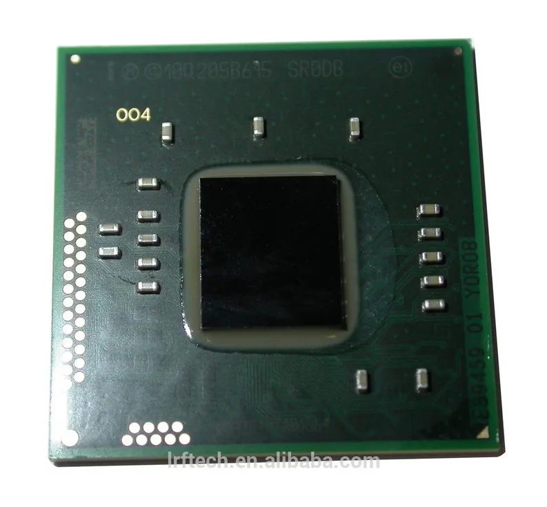 At first, these were processors selected for low power consumption, other things being equal (except that the frequencies are lower, and the case is smaller). Then they began to produce CPUs specially modified for such applications. The story can start with the i80386SL chip, which first appeared SMM (System Management Mode — system management mode), the dynamic core was replaced with a static one (i.e., to save energy, the frequency can drop to zero), and cache, memory and ISA and PI (Peripheral Interface) buses. All these changes tripled the number of transistors (from 275,000 for a regular 386SX/DX to 855,000), but the engineers felt that such a budget was justified. In addition, there were also i386CX and i386EX versions without built-in peripherals with three power saving modes.
A lot of water has flowed under the bridge, each next CPU (except for server ones) was produced both in a regular and in a mobile (sometimes even embedded) version, but all the manipulations basically consisted in adding power-saving modes to the core and selecting chips that can work on undervoltage at low frequencies.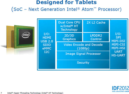 Meanwhile, competition from architectures designed specifically for mobile devices intensified: the 1990s brought PDAs (beginning with the Apple Newton MessagePad), and the 2000s brought communicators, Internet tablets (MID), and ultra mobile PCs (UMPCs). ). On top of that, it turned out that the main tasks for the user of such devices have small computing needs, so almost any CPU released after 2000 already had the necessary power for mobile applications, except, perhaps, modern games (for which just then came mobile consoles with 3D graphics).
There is a need to make a special architecture for a compact mobile device, where the main thing is not speed, but energy efficiency. In Intel, this task was taken over by the Israeli branch of the company, which had previously created a very successful family of Pentium M mobile processors (Banias and Dothan cores). In these CPUs, energy-saving principles were put at the forefront from the very beginning of development, so the dynamic shutdown of the blocks depending on their load and the smooth change in voltage and frequency became the key to the economy of the series. Pentium M looked especially bright against the background of the Pentium 4 produced at the same time, which in comparison with them seemed like hot frying pans. Moreover, operating at the same frequency, the Pentium M outperformed the «fours» in terms of performance, which is the first time in the practice of processor building — usually a mobile computer pays for its compactness with all other characteristics. However, the Pentium 4 itself was, let’s say, not very good as a universal CPU …
The success of the platform has shown that not everyone needs such a high speed, but it would be nice to save more energy. At that time (mid-2007), Intel released the «father» of our today’s heroes — the A100 and A110 processors (the Stealey core). These are 1-core 90-nm Pentium Ms with a quarter of the L2 cache (512 KB in total), greatly reduced frequencies (600 and 800 MHz) and consumption of 0.4–3 W. For comparison, standard Dothan at frequencies of 1400-2266 MHz have an energy consumption of 7. 5-21 W, low-voltage (LV subseries) — 1400-1600 MHz and 7.5-10 W, and the first introduced ultra-low voltage (ULV) — 1000-1300 MHz and 3–5 W. Reasonably believing that a modern computer spends most of its time waiting for the next keystroke or mouse shift by one more pixel, the main difference between the A100 / A110 and the ULV subseries, Intel made the ability to fall asleep very deeply when it is not necessary to count at all, due to which consumption during idle time drops in order. And the greatly reduced cache (large L2 at such frequencies is not really needed) helped to reduce the size of the chip, which made it cheaper. The size of the processor package has decreased by five times, and the total area of the CPU and chipset has been reduced by three times. As we will see later, such techniques were also used in the Atom series.
Despite the fundamentally correct goal setting, the A100/A110 remained little in demand on the market. Either 600–800 MHz turned out to be still not enough even for a simple Internet tablet, or just two chips (which is even difficult to call a model range) from the very beginning were an experimental product for testing the technology, or the processor was simply not promoted by marketers, knowing that it is being replaced by something much more advanced. .. Less than six months after the release of the A100/A110, on October 26, 2007, Intel announced the imminent release of new mobile CPUs codenamed Silverthorne and Diamondville with the Bonnell core, the future Atoms. By the way, the name Bonnell comes from the name of a hillock 240 m high in the vicinity of Austin (Texas), where a small group of Atom developers was located in the local Intel development center. “Whatever you call a yacht, so it will float.” ©Captain Vrungel
In 2004, after the cancellation of the Tejas project (the successor to the Pentium 4) it led, this group received the exact opposite task — the Snocone project to develop an extremely low-power x86 core, dozens of which will be combined into a super-efficient chip with a consumption of 100–150 W ( the future Larrabee, recently upgraded to «demonstration prototype» status). The group included several microelectronic architects from other companies, including the «sworn friend» AMD, and its head Belli Kuttanna worked at Sun and Motorola. The engineers quickly found that the various architectures available did not suit their needs, and while thinking further, at the end of the year, Intel CEO Paul Otellini told them that the same CPU would also be 1-2-core for mobile devices. Then it was hard to imagine exactly how and with what requirements such a processor would be used after the 3 years allotted for development — the management pointed to handhelds and 0.5 W of power with a high degree of risk. History has shown that almost everything was predicted correctly.
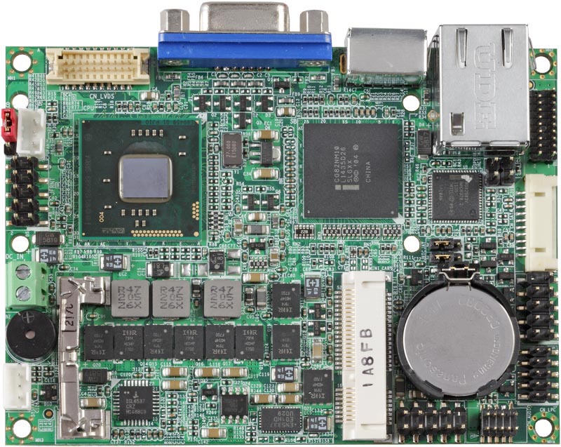
CE4100 device
Interestingly, following the Atom, in the summer of 2008, EP80579 (Tolapai) was released for embedded applications with a Pentium M core, 256 KB L2, 64-bit memory channel, a full set of peripheral controllers, frequencies of 600– 1200 MHz and consumption of 11-21 watts. And almost immediately after it — the Media Processor CE3100 (Canmore) model for digital home and entertainment: Pentium M architecture, 800 MHz frequency, 256 KB L2, three 32-bit memory controller channels, 250 MHz RISC video coprocessor and two 340 MHz DSP cores (digital signal processor) for audio. How these things were bought is not clear, because after the announcement, nothing was heard about them, including from Intel. Apparently, not very … Already after the heyday of the Atom, in September 2009th, Intel tried again and released the CE4100, CE4130 and CE4150 (Sodaville) already on the «atomic» core with a frequency of 1200 MHz, two 32-bit DDR3 channels, updated peripherals and 45 nm technology. Again, little has been heard of these highly integrated systems-on-a-chip (SOC) since then. Maybe the market is not ready to meet the hero?
CE4100 on the left, CE3100 on the right
Atom Theory
First, let’s look at the main characteristics of the processor from the consumer’s point of view. There are three of them: speed, energy efficiency, price. (True, energy efficiency is not a very “consumer” characteristic, but, nevertheless, it is the easiest way to judge some important parameters of the final device from it.) Next, we recall that an ideal CMOS microcircuit (all modern digital chips) power consumption is proportional to the frequency and the square of the supply voltage, and the peak frequency is linearly dependent on the voltage.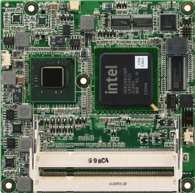 As a result, by halving the frequency, we can halve the voltage, which in theory will reduce energy consumption by 8 times (in practice, by 4–5 times). Thus, the mobile processor must be low-frequency and low-voltage. How then can he be fast? To do this, it needs to execute as many instructions as possible for each clock cycle, which most often means an increase in the number of pipelines (the degree of superscalarity) and / or the number of cores. But this leads to a sharp increase in the transistor budget, which increases the area of the chip, and hence its cost.
Thus, even theoretically it will not be possible to win on all three points (which explains the presence of such a variety of processor architectures on the market). Therefore, somewhere you have to give up positions. The historical digression says that it is necessary to pass in speed, which will make it possible to make the CPU core as simple as possible. It was on this path that the engineers from Austin went. After considering the options, they decided to return to the 15-year-old architecture, the first and last time (among Intel processors) used in the first Pentiums. Namely: the processor remains superscalar (i.e., we will have 2 instructions per cycle — but not 3-4, as in Atom’s contemporaries), loses the mechanism for shuffling instructions before execution (OoO), but acquires something that the Pentium did not have — hyperthreading technology (HT), which allows emulating the presence of two logical ones for the OS and software on the basis of one physical core. In order to explain why this choice was made, the reader is advised to first recall all the possible ways to increase CPU performance. Now let’s evaluate them in terms of energy consumption and transistor costs.
Using a multi-processor configuration in a pocket or knee device is unacceptable, but multi-core is fine if the speed of one core is not enough. At first, Intel did it in the same way as in the first 2-core Pentium 4 — by placing a pair of identical 1-core chips on a common substrate and a common bus to the chipset. Of the other shared resources, there is only a supply voltage, which is selected from a maximum of two requests. That is, the nuclei can change their frequencies separately, but fall asleep and wake up synchronously. December 2009d. Intel released the first integrated versions of Atoms, where there are 1-2 cores and a northbridge on a single chip. The southbridge remained on the board, connected to the CPU by the DMI bus, which is a little faster and more economical than the previous combination. More than two cores will not be offered to us soon, so the main high-speed emphasis is placed on their insides.
The question of increasing the frequency ceiling of Intel engineers at this stage was also not very worried, although no one was going to abandon the principle of pipeline and decoding x86 commands into internal micro-operations (mop) — this would be too radical a step back. But transition predictors, data preloaders and other auxiliary systems for filling the pipeline have become very important, because an idle pipeline that cannot execute other commands bypassing the stuck one means precious watts thrown to the ground — and Atom has all the necessary “props” made a little worse than the Pentium M and more modern Core 2, except that the buffer sizes are smaller (again, for the sake of economy).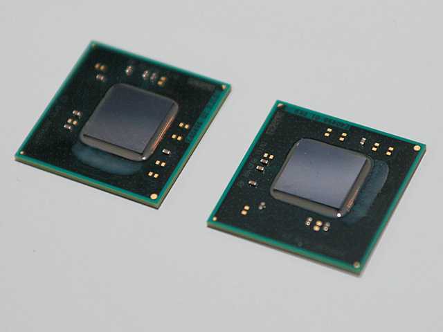 As a result, the main battle is played around the performance per clock.
Having examined the diagram of CPU acceleration options, we see that among the qualitative ways to increase performance is to increase the bit depth of scalar and vector operations, as well as complicating the instruction system with various additions with specialized instructions that perform more operations on arguments. All this is in Atom — and the latest SSSE3 instruction set at the time of development and even the 64-bit x86-64 extension. So there is enough action for the command. The whole essence of the Atom is in the number of commands per clock, i.e. in the IPC indicator.
An extensive (quantitative) way would be to increase the number of pipelines and the sizes of different caches and buffers. Obviously, starting from a certain point, it is too expensive for the transistor budget, bringing less and less acceleration from the next addition. Therefore, Intel decided to stop only at the necessary minimum. As for qualitative measures, the question is more complicated. Of the possible options, only the abundant use of mOP microfusion does not raise questions — it is necessary that as few instructions as possible generate more than one mop during decoding, occupying both pipelines and preventing the execution of two instructions per clock. Macro-merge is not implemented either because of its low efficiency (if we take the implementation in Core 2 as an example), or because of a 50% chance of triggering (because the first command to be merged must go to the first decoder, and the second to the second, and not otherwise). With a decrease in the number of cycles for executing commands, we will figure it out later.
There are technologies for maximizing the filling of conveyors. Using them at the same time will be a bit fat, so you will have to choose one thing — either the command shuffling that has been familiar to everyone for 15 years, or the younger HT, which appeared at Intel only in the latest Pentium 4 models. First of all, it should be said that when using modern compilers ( but without manual optimization) the number of consecutive instructions in the program that can be executed in parallel fluctuates around two. That is, for a 2-way (2-way) pipeline, the shuffling of commands does not seem to be needed. In addition, the pipeline can be partially filled or even completely stopped not only by the impossibility of simultaneously executing uops, but also by a particularly long cache miss or mispredicted branch. It turns out that the option of using HT as an alternative to OoO looks reasonable, although unusual for classical schemes.
Let’s also add that the so-called «reorder buffer» and «reservation stations» are rather resource-intensive blocks that have to solve the difficult task of determining free resources and interdependencies in commands that claim to be executed. The only way to do this in 1 cycle is to trade computational complexity for redundancy. For 3-4-way pipelines, this is done with hundreds and thousands of comparators that fire every cycle and check all possible combinations of uop triggers. Which, of course, requires a considerable area and a fair amount of energy. Hyperthreading, on the other hand, requires only additional buffers to store the second state of the pipeline (for the “other” thread), a duplicate register file and relatively simple logic that matches and switches flows, and the rest of the resources are shared.
The question immediately arises: if HT is such a great thing, why isn’t it implemented everywhere? Firstly, for a 3-4-thread superscalar with OoO, the average pipeline load is such that the second thread of commands will increase the speed by only 10 percent. After all, its execution also needs free resources, and if both programs stumble over the same thing (for example, , lack of cache), nothing will help them. Secondly, a single-threaded application cannot be accelerated this way, although the overall system responsiveness will improve. That is, the overall acceleration will greatly depend on the selection of a pair of running programs (here we assume everywhere that “hyper-” means “two-”). However, for the small price paid in transistors, this is quite good. Intel, however, gives other figures, focusing on savings: by increasing consumption by 20%, turning on HT gives an acceleration of as much as 30–50% (let’s leave these figures, especially the second one, on the conscience of the applicant).
Atom’s Core
Having done the necessary theoretical preparation, we finally got to the actual architecture. Its strong simplification made it possible to reduce the number of transistors in the CPU to 47 million (of which 13.8 million per core, including both L1 caches), and the area to 26 mm² (a 45-nanometer process technology is used with 9 layers of copper tracks, metal gates and gate dielectrics with high permeability). For comparison, the 90-nanometer Pentium M occupied 84 mm², but there is four times the L2 cache. The Pentium M core occupies approximately 35 million transistors, and Core 2 — 50 million. Although, of course, the atom cannot stand comparison with the first Pentium (3. 3 million), it cannot be called quite simple either, which is indirectly seen from the size of the article . 🙂
The Atom is most simply described as a very heavily modernized Pentium, but that can be said about almost any modern processor. Most of all, he has in common with the 15-year-old old man 2-way superscalarity and the absence of OoO (the first drafts of Atom were 1-way at all, like 486), but almost everything else distinguishes him. First of all, the “atomic conveyor” has as many as 16 stages. For comparison, the first Pentium has 5 of them (8 for the real part), the Pentium M and Core Solo/Duo have 14, and the Core 2 has 16 (measured when the pipeline was dropped). Why so many? A long conveyor allows you to raise the frequency ceiling, but here it is not necessary at all. There are 3 stages for accessing the L1D cache, and all commands go through them, including those that do not go «out» — this solution greatly simplifies pipeline management and is used in all «ordered» (in-order) architectures. It is also possible to turn off stages in more detail with their simple to save energy and «thin» switching between streams (with HT on) individual stages and their small groups. However, the gain in watts and instructions executed is easily offset by a longer delay when the pipeline is reset due to a mispredicted branch.
Therefore, the transition predictor, from which the pipeline begins, is only slightly inferior to its “colleagues”. This is a 2-level adaptive predictor with a global navigation history table (GBHT) at 4096 cells and 12-bit indexing. The jump address buffer (BTB) has only 128 cells, organized as 32 4-way sets (tens of times smaller than modern desktop and even «classic» mobile CPUs). There is no special predictor for loops or indirect jumps. Like all modern kernels, there is a stack of return addresses from subroutines for 8 cells (plus 2 buffer cells in the predictor). Reduced size tables save space, but trip up programs with a large number of jumps, even well-predicted ones or even unconditional ones (including subroutine calls). Moreover, switching to the second stream may not help, because both streams share these buffers and tables. The prediction occurs with the tempo 1 time in 2 bars, but if it turns out to be wrong, the penalty will be 13 bars. If the prediction of the behavior is correct, but the address has already been squeezed out of the tiny BTB, you have to wait 7 cycles.
Instructions are loaded in 8-byte chunks from the L1I cache into the predecoder’s double buffer, 16 bytes per stream, and in 1-stream mode, both buffers can serve a single stream, subject to alignment rules, reaching a maximum rate of 10–11 bytes/clock. This figure is somewhat redundant, because even for their 4-way superscalars (and even with macro-fusion, which occasionally allows decoding the 5th instruction), Intel still uses a 16-byte load — although the average instruction length (especially in 64-bit mode and with abundant use of various SSEs) is about to exceed 4 bytes.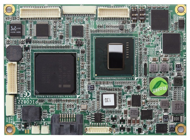
Manufacturers stuffed modern x86 CPUs with a cumbersome command system with an extremely complex decoding scheme, so decoders are forced to spend a large number of transistors and energy even on such a seemingly elementary operation as determining the instruction length (more precisely, this is done by a separate stage — the predecoder length gauge or ILD ) because you need to process commands with multiple prefixes. For Atom, the number of prefixes greater than three will cause a serious delay. That is, for commands of the SSE2 / 3 set (1-2 prefixes) in 64-bit mode (1 more) this is enough, but for the more recent SSSE3 (or some version of SSE4, if Intel wants to add it to Atom) — not anymore.
To speed up length measurements, a pre-decode tag buffer is associated with L1I, where the marking of command boundaries is stored. This solution is justified to save energy when executing code that has already been encountered and is similar to that used in AMD K7-K10 cores, where ILD works when reading from L2 to L1I — however, this scheme is designed to speed up the main decoding. But in Atom, markup bits are determined and sent to the buffer only at the first execution of the cached code, which happens at a speed of 3 cycles / byte (for AMD — 4 bytes / cycle). The reason for this sluggishness is a very simple sequential length gauge. At the same time, all teams always go through the ILD stage, just those that met earlier, having read the finished markup, go through it “throughout”, without straining the transistors — and again, savings leads to an extension of the pipeline.
Commands are decoded by two simple translators and one microsequencer. This is somewhat different from the usual scheme, where one of the translators is complex, because it generates more than one uop per cycle (usually 3-4, according to the number of pipelines). All translators decode one instruction per clock. The microsequencer issues several uops (for the Atom, of course, no more than two), but within a few cycles and only for particularly complex commands that require microcode. However, according to Intel, only 4% of commands will require more than 1 uop — 16% of commands undergo microfusion, including such relatively complex ones as Load-Op-Store (with a modifier in memory), which previously required 2-3 uop (from other x86 architectures, only AMD K10 can do this). That is, for the Atom, microfusion reduced the number of microcode accesses by a factor of five. Thus, the desire to split commands into simple RISC operations to speed up execution, which is obvious today and 15 years ago (this is what P6, aka Pentium Pro, differed from P5), in this case has reversed — for lack of the ability to shuffle commands, it is extremely wasteful to score the entire conveyor with mops (especially since it is already very narrow) — and the speed is enough without it.
The output of the decoder is connected to a 32 mop queue, which is statically divided in two when HT is enabled. The entire front-end (the “head of the pipeline” from the predictor to the queue of uops) can work in isolation from the back-end (executive “tail”) in case of data delays or the execution of a long command, filling the queue with uops in reserve.
The Power of the Atom
So, how does Atom process data so that it is very economical, low on transistors and not very slow? Execution begins with the fact that from the queue of uops 1-2, commands are transferred to two execution clusters — a scalar integer (general purpose) and a vector-real one (a scheme more similar to the design of AMD K7-K10 cores). Exchange between clusters (for example, when converting formats) requires 4–5 delay cycles. The L1D cache is connected to the common cluster, so the communication with the memory for the second cluster is longer. Each cluster can execute two commands per cycle, but no more than two in total, since cluster launch ports are closely connected.
Both ports can execute the most common commands — copying between registers of the same type and simple integer operations in the ALU (including vector ones). But only port 0 can perform memory exchange, shifts, shuffles and repacks, multiplications, divisions, and other complex arithmetic. Port 1 exclusively got transitions and real additions (including vector additions). Among other things, this means that the already familiar 2-port access to L1D, even in an abbreviated form (write + read), is absent — the cache is strictly one-port, which was last used in Intel 486.
Since there is no shuffling of instructions before execution, programmers (and compilers) will have to learn the rules for instruction pairing. However, they differ significantly from those available in the Pentium:
- A launched pair of uops always belongs to the same thread. It will not work to launch one “own” and one “alien” one.
- Two instructions must go in the code in a row — except for the permissible case when the first is a branch instruction pointing to the second.
- The second (in the course of the program) instruction cannot read the register modified by the first one — except for the conditional jump, which can be the second one, since it can read the flags changed in the same cycle by the first mop.
- Commands must not write to the same register (except for flags) — even if it is completely overwritten.
- Commands must use different ports.
- Commands that load the functional units (FU) of both ports are not paired. For example, real-time memory addition uses port 0 for address computation and memory access, and port 1 for addition itself.
- Two scalar real instructions for the x87 stack not only do not pair (even on different ports), they also give an additional delay of 1 cycle — even a couple of FNOPs that do nothing.
From this essentially devastating list of forbidding conditions, it becomes clear that the Atom’s superscalarity is not exactly nominal, but even «pretentiously curved.» It is unlikely that Intel’s microarchitects have become drastically stupid, but the pursuit of extreme simplicity and energy efficiency has brought the architecture to the point of absurdity, when one of the two pipelines will often be idle due to too strict pairing rules. Some relief is that running commands with different execution durations does not result in penalties. Similarly — processing data of a different type (for vector commands). For example, you can use the MOVAPS instruction for integers.
The most common stumbling block for in-order architectures is a cache miss, which can take 10-200 cycles to service. In case of a miss, such a CPU simply waits (at best, suspending clocking to save money), and the architecture with OoO executes commands accumulated in the shuffle buffer and data-independent from the result of the problematic command. The situation is so common that having no shuffling mechanism at all seemed unjustified to Intel engineers — and they came up with an additive called Safe Instruction Recognition (safe command recognition). It still gives the processor some freedom in handling commands, allowing them to be executed out of order, and in fact it is an OoO mechanism that works on the scale of only two instructions, one of which must be real, and the second must be integer.