with 4nm, 3nm, 20A and 18A?!
In today’s Intel Accelerated event, the company is driving a stake into the ground regarding where it wants to be by 2025. CEO Pat Gelsinger earlier this year stated that Intel would be returning to product leadership in 2025, but hasn’t yet explained how this is coming about – that is until today, where Intel has disclosed its roadmap for its next five generations of process node technology leading to 2025. Intel believes it can follow an aggressive strategy to match and pass its foundry rivals, while at the same time developing new packaging offerings and starting a foundry business for external customers. On top of all this, Intel has renamed its process nodes.
The Short Answer:
If you only take one thing away from this article, I’m going to put it here front and center. Here is what we’re seeing for Intel’s roadmaps, based on their disclosures today.
As always, there is a difference between when a technology ramps for production and comes to retail; Intel spoke about some technologies as ‘being ready’, while others were ‘ramping’, so this timeline is simply those dates as mentioned. As you might imagine, each process node is likely to exist for several years, this graph is simply showcasing the leading technology from Intel at any given time.
If you want the details on this graph, then read on.
Earlier this year, CEO Pat Gelsinger announced Intel’s new IDM 2.0 strategy, consisting of three elements:
- Build (7nm)
- Expand (TSMC)
- Productize (Intel Foundry Services)
The goal here is to continue to work on Intel’s process node technology development, going beyond the current 10nm designs in production today, but simultaneously using other foundry services from partners (or competitors) to regain/retain Intel’s position in its processors that drive a lot of the company revenue. The third element is IFS, Intel’s Foundry Services, where Intel is committing in a big way to opening up its manufacturing facilities to external semiconductor business.
Underpinning (1) and (3) is how Intel executes on its own process node development. While in Intel’s recent Q3 2021 earnings call CEO Gelsinger confirmed that Intel is now producing more 10nm wafers in a day than 14nm wafers, marking a shift in confidence between the two designs, it is no secret that Intel has had difficulty in transitioning from its 14nm process to its 10nm process. On June 29th this year, Intel also stated that its next generation 10nm product requires additional validation time to streamline deployment on enterprise systems for 2022. Note that at the same time, TSMC has surpassed Intel by shipping at capacity with its equivalent designs (called 7nm) and its leading edge (5nm) designs that surpass Intel’s performance.
As with the previous announcement in March, Intel is reaffirming that it intends to return to leadership performance in semiconductors in 2025. This will enable both the company to compete better as it builds its own products (1) but also offer a wider portfolio of performance and technologies for its future IFS customers (3). To do this, it is realigning the roadmap for its future process node technologies to be more aggressive with improvements, yet at the same time more modular with its technology to enable faster transitions.
Leading up this plan is Dr. Ann B Kelleher, who was named SVP and GM of the Technology Development division at Intel last year. This division is where all the research and development of Intel’s future process node technologies and enhancements comes from – it used to be part of Intel’s System Architecture Group, however it was split in July 2020 to re-establish a focus purely on Technology Development. Dr. Kelleher’s background involves process research in academia, followed by 26 years at Intel as a process engineer, moving up to managing Fab 24 in Ireland, Fab 12 in Arizona, Fab 11X in Rio Rancho, before landing in HQ in Oregon as the GM of Manufacturing and Operations.
Her experience covering both fab-scale production and process node research is going to be critical for Intel’s future plans. In discussing with Kelleher ahead of today’s announcements, she stated that she has implemented fundamental changes when it comes to supplier approach, ecosystem learnings, organizational changes, modular design strategies, contingency plans, and realigning the Technology Development Team into a more streamlined outfit ready to execute. These include key personnel such as Sanjay Natarajan as SVP and GM of Logic Development (one of Intel’s recent rehires) and Babak Sabi as CVP and GM of Assembly/Test Development
Intel is today defining ‘technology leadership by 2025’ as defined by the metric of performance per watt. We asked Intel is a pre-briefing what that means for peak performance, which is often a metric we care about for end product design, and the answer was that «peak performance remains a key part of Intel’s strategic development».
Intel Renames The Nodes: ‘Mine is Smaller’
The problem with simply posting Intel’s roadmap here is that the news is two-fold. Not only is Intel disclosing the state of its technology for the next several years, but the names of the technology are changing to better align with common industry norms.
It is no secret that having «Intel 10nm» being equivalent to «TSMC 7nm», even though the numbers actually have nothing to do with the physical implementation, has ground at Intel for a while. A lot of the industry, for whatever reason, hasn’t learned that these numbers aren’t actually a physical measurement. They used to be, but when we moved from 2D planar transistors to 3D FinFET transistors, the numbers became nothing more than a marketing tool. Despite this, every time there’s an article about the technology, people get confused. We’ve been talking about it for half a decade, but the confusion still remains.
To that end, Intel is renaming its future process nodes. Here’s the roadmap image, but I’ll be breaking it down piece by piece.
2020, Intel 10nm SuperFin (10SF): Current generation technology in use with Tiger Lake and Intel’s Xe-LP discrete graphics solutions (SG1, DG1). The name stays the same.
2021 h3, Intel 7: Previously known as 10nm Enhanced Super Fin or 10ESF. Alder Lake and Sapphire Rapids will now be known as Intel 7nm products, showcasing a 10-15% performance per watt gain over 10SF due to transistor optimizations. Alder Lake is currently in volume production. Intel’s Xe-HP will now be known as an Intel 7 product.
2022 h3, Intel 4: Previously known as Intel 7nm. Intel earlier this year stated that its Meteor Lake processor will use a compute tile based on this process node technology, and the silicon is now back in the lab being tested. Intel expects a 20% performance per watt gain over the previous generation, and the technology uses more EUV, mostly in the BEOL. Intel’s next Xeon Scalable product, Granite Rapids, will also use a compute tile based on Intel 4.
2023 h3, Intel 3: Previously known as Intel 7+. Increased use of EUV and new high density libraries. This is where Intel’s strategy becomes more modular – Intel 3 will share some features of Intel 4, but enough will be new enough to describe this a new full node, in particular new high performance libraries. Nonetheless, a fast follow on is expected. Another step up in EUV use, Intel expects a manufacturing ramp in the second half of 2023 with an 18% performance per watt gain over Intel 4.
2024, Intel 20A: Previously known as Intel 5nm. Moving to double digit naming, with the A standing for Ångström, or 10A is equal to 1nm. Few details, but this is where Intel will move from FinFETs to its version of Gate-All-Around (GAA) transistors called RibbonFETs. Also Intel will debut a new PowerVia technology, described below.
2025, Intel 18A: Not listed on the diagram above, but Intel is expecting to have an 18A process in 2025. 18A will be using ASML’s latest EUV machines, known as High-NA machines, which are capable of more accurate photolithography. Intel has stated to us that it is ASML’s lead partner when it comes to High-NA, and is set to receive the first production model of a High-NA machine. ASML recently announced High-NA was being delayed- when asked if this was an issue, Intel said no, as the timelines for High-NA and 18A are where Intel expects to intersect and have unquestioned leadership.
Intel has confirmed to us that Intel 3 and Intel 20A will be offered to foundry customers (but hasn’t stated if Intel 4 or Intel 7 will be).
To bring this altogether in a single table, with known products, we have the following:
| Intel’s Process Node Technology | ||||
| Old Name | New Name | Roadmap | Products | Features |
| 10SF | 10SF | Today | Tiger Lake SG1 DG1 Xe-HPC Base Tile Agilex-F/I FPGA |
SuperMIM Thin Film Barrier Volume 10nm On sale today |
| 10ESF | Intel 7 | 2021 h3 products | Alder Lake (21) Raptor Lake (22)? Sapphire Rapids (22) Xe-HP Xe-HPC IO Tile |
10-15% PPW Upgraded FinFET ADL in Ramp today |
| 7nm | Intel 4 | 2022 h3 ramp 2023 h2 products |
Meteor Compute Tile Granite Compute Tile |
20% PPW vs 7 More EUV Silicon in Lab |
| 7+ | Intel 3 | 2023 h3 products | — | 18% PPW vs 4 Area Savings More EUV New Perf Libraries Faster Follow On |
| 5nm | Intel 20A | 2024 | — | RibbonFET PowerVia |
| 5+ | Intel 18A | 2025 | Unquestioned Leadership | 2nd Gen Ribbon High NA EUV |
One of the issues here is the difference between a process node being ready, ramping production for product launches, and actually being made available. For example, Alder Lake (now on Intel 7nm) is due to come out this year, but Sapphire Rapids is going to be more of a 2022 product. Similarly, there are reports of Raptor Lake on Intel 7 coming out in 2022 to replace Alder Lake with the tiled Meteor Lake on Intel 4 in 2023. While Intel is happy to discuss process node development time frames, product timeframes are not as open (as no doubt customers would get frustrated if the time stated is missed).
Why The Nodes Were Renamed
So as stated before, one element of renaming the nodes is due to matching parity with other foundry offerings. Both TSMC and Samsung, competitors to Intel, were using smaller numbers to compare similar density processes. With Intel now renaming itself, it gets more in-line with the industry. That being said, perhaps sneakily, Intel’s 4nm might be on par with TSMC’s 5nm, reversing the tables. By 3nm we expect there to be a good parity point, however that will depend on Intel matching TSMC’s release schedule.
Rather than throw process node names everywhere, it is typical to refer to peak quoted transistor densities instead. Here is the table we published in our recent IBM 2nm news post, but with an updated shift on Intel’s naming.
| 2021 Peak Quoted Transistor Densities (MTr/mm2) | ||||
| AnandTech Process Name |
IBM | TSMC | Intel | Samsung |
| 22nm | 16.50 | |||
| 16nm/14nm | 28.88 | 44.67 | 33.32 | |
| 10nm | 52.51 | 100.76 | 51.82 | |
| 7nm | 91.20 | 100.76 | 95.08 | |
| 5/4nm | 171.30 | ~200* | 126. 89 89 |
|
| 3nm | 292.21* | |||
| 2nm / 20A | 333.33 | |||
| Data from Wikichip, Different Fabs may have different counting methodologies * Estimated Logic Density |
||||
Exactly where Intel’s new 4nm and below will end up is yet to be disclosed, as numbers with stars alongside are based on estimates by the respective companies.
It has been expected for a while that Intel would be realigning its process node naming. Behind closed doors, I personally have been lobbying for it for a while, and I know that a few other journalists and analysts have been suggesting it to Intel as well. Some responses we received were related to apathy – one executive told me that «our customers that care about this actually know the difference», which is true for sure, but what we’re talking about here is more about perception in the wider ecosystem for enthusiasts and financial analysts who might not be up to speed. It is more or less a branding exercise, and I also told Intel that they are going to have to expect a mixed response – some voices might interpret the move as Intel trying to pull one over on the market, for example. But they’re going to have to live with it, as these are the new names.
Meanwhile, despite Intel’s struggles with 10nm, it is still a process node in production and in volume production, in use for both consumer and enterprise devices, and it’s coming to desktops very soon. Even though it has some stiff competition from other players, it is still an offering in the market, and for those that want to compare process node densities using these names, it should have a moniker to avoid confusion. I am applauding that Intel is doing it sooner rather than later.
One key point to note is that the new Intel 7 node, which was formerly the 10ESF node, is not necessarily a «full» node update as we typically understand it. This node is derived as an update from 10SF, and as the diagram above states, will have ‘transistor optimizations’. Moving from 10nm to 10SF, that meant SuperMIM and new thin-film designs giving an extra 1 GHz+, however the exact details from 10SF to the new Intel 7 is unclear at this point. Intel has however stated that moving from Intel 7 to Intel 4 will be a regular full node jump, with Intel 3 using modular parts of Intel 4 with new high-performance libraries and silicon improvements for another jump in performance.
We asked Intel if these process nodes will have additional optimization points, and were told that they will – whether any of them will be explicitly productized will depend on the features. Individual optimizations may account for an additional 5-10% performance per watt, and we were told that even 10SF (which keeps its name) has had several additional optimization points that haven’t necessarily been publicized. So whether these updates get marketed as 7+ or 7SF or 4HP is not known, but as with any manufacturing process as updates occur to help improve performance/power/yield, they get applied assuming the design adheres to the same rules.
«Isn’t Intel Just Trying To Pull The Wool Over Our Eyes?»
No.
The problem here is that there is no consistent node naming between foundries. Intel has been saving any number change for major advances in its node manufacturing technology, instead using +/++ to signify improvements. If we compare this to TSMC and Samsung, both of whom have been happy to give half-node jumps new numbers entirely.
For example, Samsung’s 7LPP is a major node, however 6LPP, 5LPE and 4LPE are all iterative efforts on the same design (arguably also iterative of 8LPP), with 3GAE being the next major jump. Compare this to Intel, who was planning 10nm to 7nm to 5nm as major process node jumps – so while Samsung had one jump planned and 4 sub-variants (or more), Intel had two major jumps. Similarly, TSMC’s 10nm was a half-node jump over 16nm, while 16nm to 7nm was the full node – Intel made 14 to 10 to 7 as full nodes.
Intel stuck to its guns a long while, and delays to 10nm effectively hurt it in a multiplicative fashion. For example, if Intel had labeled 14+ as 13nm, and 14++ as 12nm, perhaps it wouldn’t be so bad. I mean, yes Intel should expect some hurt for 10nm being late, but when other foundries were showcasing smaller steps as full number jumps, it became a marketing and media nightmare. 14++++ became an industry joke, and coupled with how every time when they talked about future process nodes they had to cite the equivalent TSMC of Samsung process, it got a bit too much. It had to be explained every time, as new people come into the industry.
I’ve lobbied Intel to adjust its naming for a while, and I know other peers have as well. When we refer to Intel 7 from now on, we can draw equivalents to TSMC 7nm (even if TSMC is shipping 5nm in volume) without having to extensively explain differences in a simple name. This isn’t Intel pulling the wool over your eyes, or trying to hide a bad situation. This is Intel catching up to the rest of the industry in how these processes are named. To add to this, it’s a good thing that Intel is only renaming future nodes that haven’t reached the market yet.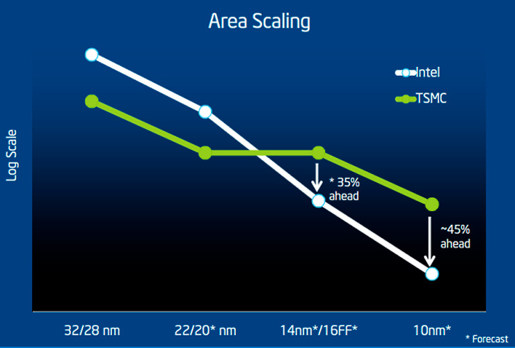
This is a multi-page article!
Click the dropdown below for more pages, including
- This Page, New Node Names
- A Sidebar on Intel EUV and becoming ASML Lead Partner
- New for 2024: RibbonFETs and PowerVias
- Next Gen EMIB and Foveros Packaging
- Customers Customers Customers
Sidebar on Intel EUV and ASML
Intel’s Process Roadmap to 2025, with New Node NamesSidebar on Intel EUV and ASMLNew Technology Features for 2024: RibbonFETs and PowerViasIntel’s Next Generation Packaging: EMIB and FoverosCustomers
Tweet
Intel Unveils 2021-2029 Process Roadmap
Back in May, Intel unveiled their process roadmap, highlighting their target plans up till 2023, but an even more detailed manufacturing roadmap has been revealed by Anandtech which shows a process roadmap path all the way up to 2029.
Intel Manufacturing Roadmap For The Next 10 Years Unveiled — 7nm in 2021, 5nm in 2023, 3nm in 2025, 2nm in 2027 and 1.
 4 nm in 2029, Brand New Features and Back Porting
The roadmap is stated to have been unveiled at the IEEE International Electron Devices Meeting by one of Intel’s partners who stated that the said slide was first showcased by Intel themselves back in September. Intel already gave us a deep dive of their 7nm process plans but this slide goes even further than that. It’s a 10-year roadmap for what’s to come so let’s see what Intel has to offer us in the coming years.
Intel’s Process and Manufacturing Roadmap for the next 10 years shows 10nm, 7nm, 5nm, 3nm, 2nm, and 1.4nm. (Image Credits: Anandtech)
10nm to 1.4nm in The Next 10 Years
Starting off with the process roadmap, Intel will be following a 2-year cadence for each major node update. We got a soft launch of 10nm (10nm+) in 2019 which will be followed by 7nm in 2021, 5nm in 2023, 3nm in 2025, 2nm in 2027 and 1.4nm in 2029. What’s interesting here is that this 2-year cadence is referred to as the optimal cost-performance path by Intel themselves. So it would be Intel’s priority to follow this path, but there’s also a yearly cadence for the + / ++ nodes that offer more performance leverage and scalability opportunities on an existing node.
Before we talk about the optimized nodes for each process, we should focus on the key features that each major node update has to offer. For 7nm, Intel is saying the biggest feature is that it is made using EUV (Extreme ultraviolet lithography) technology. Similarly, all other major nodes will come with new features, but Intel hasn’t explicitly stated what new features we could expect. At the same time as Intel introduces their 10nm++ products, they will also have production and launch planned for their next-gen 7nm process node. The 10nm and 7nm nodes were already detailed by Intel during their 2019 Investors Meeting.
2 of 9
Intel 10nm, 10nm+ and 10nm++
Starting off with the 10nm family, Intel has clarified that their 10nm process node can deliver some major enhancements to performance per watt. Compared to 14nm++, the first iteration of 10nm is shown to be a good leap in efficiency and Intel plans to provide enhanced variants of 10nm moving forward with 10nm+ in 2019, 10nm++ in 2020, and 10nm+++ in 2021. Some of the major upgrades that 10nm would deliver include:
- 2.7x density scaling vs 14nm
- Self-aligned Quad-Patterning
- Contact Over Active Gate
- Cobalt Interconnect (M0, M1)
- 1st Gen Foveros 3D Stacking
- 2nd Gen EMIB
Intel 7nm, 7nm+ and 7nm++
At the same time as Intel introduces their 10nm+++ products, they will also have production and launch planned for their next-gen 7nm process node. Intel would continue to offer optimizations of the 7nm process node with 7nm+ in 2022 and 7nm++ in 2023. Just like 10nm, 7nm will deliver a good list of enhancements over 10nm which will include:
- 2x density scaling vs 10nm
- Planned intra-node optimizations
- 4x reduction in design rules
- EUV
- Next-Gen Foveros & EMIB Packaging
Do note that 10nm is the only process with a +++ optimization since it is already on 10nm+ in 2019. 1.4nm in 2029 looks to be very promising but Intel has had previous roadmaps stating that said we would get 10nm by 2015 and nm by 2017. But, more recently, Intel’s CEO, Bob Swan, stated that his company is all set to tackle TSMC with their first 7nm products tackling TSMC’s 5nm by Q4 2021 and expects to hit 5nm which he states is equivalent to TSMC’s 3nm node by the second half of 2024 and product availability in 2025.
Back Porting To Each Tail-End Optimization Node
The slide also talks about back porting which has been one of the interesting topics to discuss in recent months considering all the ruckus surrounding 14nm and 10nm nodes. Each major node has been shown to include at least two optimizations. 10nm+ will get 10nm++ and 10nm+++, 7nm will get 7nm+ (2022) and 7nm++ (2023), 5nm will get 5nm+ (2024) and 5nm++ (2025), 3nm will get 3nm+ (2026) and 3nm++ (2027) while 2nm will also get 2nm+ (2028) and 2nm++ (2029). There’s no optimized path for 1.4nm mentioned but then again, this slide only covers a 10-year roadmap so you can in the least expect an optimized node path for 1. 4nm too.
So each major node will be followed by an optimized ‘+’ node in the coming year and a further tail-end optimized ‘++’ node after that. Here’s the interesting thing, the ‘++’ or in the case of 10nm, +++ node, will launch alongside the next major node. The optimized node will have some advantages over the new node such as frequency and scalability from the previous two updates along with a higher number of yields.
So here, Intel can decide to make some interesting choices as they have multiple paths to choose from on each node generation. Now, given the timeframe of this roadmap, Intel may already have decided what’s next for 10nm and 7nm.
A picture a wafer from Intel’s foundry that was fabricated on the 14nm process.
Intel also talks about back porting on an older yet optimized node. A 7nm product can be back ported to 10nm+++, a 5nm product can be back ported to 7nm++, a 3nm product can be back ported to 3nm++ and a 2nm product can be back ported to 3nm++. There’s no back porting mentioned for the 1. 4nm node.
There have been recent rumors and talks regarding Intel back porting a 10nm++ product (Tiger Lake) to 14nm+++ (Rocket Lake). Substantial evidence has been found, but since the product is aiming a 2021 launch, there’s no official word from Intel on the matter. But, given that this roadmap talks about back porting, we may indeed see Rocket Lake CPUs featuring a back port of the Willow Cove cores that are to utilize a 10nm++ node on the mobility platform.
New Naming Scheme, 10nm ESF Now Intel 7, 7nm Now Intel 4, Intel 3, Intel 20A & Beyond
During its IDM 2.0 keynote, Intel’s CEO, Pat Gelsinger, unveiled his company’s brand new process roadmap along with a refreshing new naming scheme for next-generation nodes. The brand new roadmap covers all nodes and the respective products that we can expect to enter manufacturing and production through 2025 and beyond.
Intel Process Roadmap & Innovation Roadmap Highlights Brand New Node Naming Scheme, Drops ‘++’ & ‘SuperFin’ Brandings
Intel is restructuring as a whole under its new leadership and it looks like the process nodes, that have been confusing over the past few years, will finally be understandable for the general public. Intel recently has its 10nm SuperFin process node which is an enhanced variant of the Intel 10nm (++) node utilized by Ice Lake chips. Currently, Intel has both 10nm and 14nm chips within mobile and desktop platforms but that’s going to change later this year when Intel finally brings forth its Alder Lake and Sapphire Rapids lineup.
Under IDM 2.0, our factory network continues to deliver and we are now manufacturing more 10-nanometer wafers than 14-nanometer. As 10-nanometer volumes ramp, economics are improving with 10-nanometer wafer cost 45% lower year-over-year with more to come.
via Intel
Intel 7 Process Node (Previously 10nm Enhanced SuperFin)
So first up, we have Intel 7, a new name for the company’s 10nm Enhanced SuperFin process node. This node was going to power Intel’s Alder Lake Client and Sapphire Rapids Server lineup. Based on what Intel has stated, the node will offer a 10-15% performance per watt gain over 10nm SuperFin and feature FinFET transistor optimizations. Intel 7 is ready for volume production and the first products are expected to land on market by Q4 2021
Intel 7 delivers an approximately 10% to 15% performance-per-watt increase versus Intel 10nm SuperFin, based on FinFET transistor optimizations. Intel 7 will be featured in products such as Alder Lake for client in 2021 and Sapphire Rapids for the data center, which is expected to be in production in the first quarter of 2022.
2 of 9
Intel 4 Process Node (Previously 7nm)
Intel 4 is also something that the company has previously referred to as its 7nm process node. This is a much hyped-up node as it powers several next-generation products including Ponte Vecchio & along with that, we have Meteor Lake for Client and Granite Rapids for datacenters. Intel is claiming a 20% performance per watt gain for Intel 4 over Intel 7. In addition to these, Intel 4 will deliver a good list of enhancements over 10nm which will include:
- 2x density scaling vs Intel 7
- Planned intra-node optimizations
- 4x reduction in design rules
- EUV
- Next-Gen Foveros & EMIB Packaging
2 of 9
The node will also make full use of EUV Lithography and already has products taping out such as the Meteor Lake Compute Tile which was taped out during the previous quarter. Granite Rapids will also feature a multi-compute tile design and its main Granite Rapids core will be fabricated on the Intel 4 node.
Intel 4 fully embraces EUV lithography to print incredibly small features using ultra-short wavelength light. With an approximately 20% performance-per-watt increase, along with area improvements, Intel 4 will be ready for production in the second half of 2022 for products shipping in 2023, including Meteor Lake for client and Granite Rapids for the data center.
Intel 3 Process Node (An Intel 4 Optimization?)
Moving beyond Intel 4, the company plans to launch its Intel 3 process node which would be ready for manufacturing products by the second half of 2023. Based on everything that Intel has listed, it looks like Intel 3 is a generational optimization of Intel 4 as it delivers an 18% performance per watt gain, offers denser HP libraries, increases the intrinsic driver current, increased EUV use & reduces via resistance.
It looks like everything beyond Meteor Lake (Lunar Lake) and Granite Ridge (Diamond Rapids) could utilize the Intel 3 process node though we are talking about products that would launch in 2024 or even 2025 by the earliest so there’s a long way to go.
Intel 3 leverages further FinFET optimizations and increased EUV to deliver an approximately 18% performance-per-watt increase over Intel 4, along with additional area improvements. Intel 3 will be ready to begin manufacturing products in the second half of 2023.
Intel 20A Process Node & Beyond (A True Next-Gen Node)
Intel has gone ahead to talk about its post-nanometer era with a new product it is referring to as Intel 20A. The Intel 20A starts the Angstrom era (A for Angstrom) which is equal to 10⁻¹⁰ m or 1A = 0.1nm. This is just a cool way of saying 2nm but given how small nodes have gotten and the fact that we are heading down to decimal spaces within this decade, Intel decided a new measuring unit was needed.
2 of 9
So Intel 20A (2nm) is going to offer breakthrough innovations when it enters the early production phase by 1H 2024. The 20A node is expected to feature brand new RibbonFET transistors that will replace the existing FinFET architecture and also deliver new interconnect innovations, one of which is known as PowerVia. Intel is also expanding upon its Forveros technologies with Omni and Direct. Forveors Omni will be featured in products that package high-performance compute tiles while Forveors Direct will allow multi-tier interconnector resistance through a copper to copper bond. Forveros as a whole will be updated to deliver increased bandwidth through next-gen inter-connect solutions.
2 of 9
Intel 20A ushers in the angstrom era with two breakthrough technologies, RibbonFET and PowerVia. RibbonFET, Intel’s implementation of a gate-all-around transistor, will be the company’s first new transistor architecture since it pioneered FinFET in 2011.
The technology delivers faster transistor switching speeds while achieving the same drive current as multiple fins in a smaller footprint. PowerVia is Intel’s unique industry-first implementation of backside power delivery, optimizing signal transmission by eliminating the need for power routing on the front side of the wafer. Intel 20A is expected to ramp in 2024.
- Foveros Omni ushers in the next generation of Foveros technology by providing unbounded flexibility with performance 3D stacking technology for die-to-die interconnect and modular designs. Foveros Omni allows die disaggregation, mixing multiple top die tiles with multiple base tiles across mixed fab nodes and is expected to be ready for volume manufacturing in 2023.
- Foveros Direct moves to direct copper-to-copper bonding for low-resistance interconnects and blurs the boundary between where the wafer ends and where the package begins. Foveros Direct enables sub-10 micron bump pitches providing an order of magnitude increase in the interconnect density for 3D stacking, opening new concepts for functional die partitioning that were previously unachievable.
Foveros Direct is complementary to Foveros Omni and is also expected to be ready in 2023.
Intel Process Roadmap
| Process Name | Intel 10nm SuperFin | Intel 7 | Intel 4 | Intel 3 | Intel 20A | Intel 18A |
|---|---|---|---|---|---|---|
| Production | In High-Volume (Now) | In Volume (Now) | 2H 2022 | 2H 2023 | 2H 2024 | 2H 2025 |
| Perf/Watt (over 10nm ESF) | N/A | 10-15% | 20% | 18% | >20%? | TBA |
| EUV | N/A | N/A | Yes | Yes | Yes | High-NA EUV |
| Transistor Architecture | FinFET | Optimized FinFET | Optimized FinFET | Optimized FinFET | RibbonFET | Optimized RibbonFET |
| Products | Tiger Lake | Alder Lake Raptor Lake Sapphire Rapids Emerald Rapids Xe-HPG? |
Meteor Lake Xe-HPC / Xe-HP? |
Granite Rapids Sierra Forest TBA |
Arrow Lake Diamond Rapids? TBA |
Lunar Lake Nova Lake TBA TBA |
As for products based on the Intel 20A process node, don’t expect them to be a reality prior to 2025. Also, based upon the older roadmaps and where 20A is positioned, it looks to be either a rename of Intel’s 5nm or 3nm process node. but more scaled up to add in the ‘+’ optimizations which have been excluded from now onwards.
Intel doesn’t stop at 20A though, they go on to discuss next-generation nodes through 2025 and beyond which would include 18A. The 18A node is already in development for early 2025 and will feature refinements to the RibbonFET architecture to deliver another major leap in transistor and chip performance.
Intel’s Process and Manufacturing Roadmap for the next 10 years shows 10nm, 7nm, 5nm, 3nm, 2nm, and 1.4nm. (Image Credits: Anandtech)
These new innovations and naming schemes are great to avoid the mess that Intel was headed into just a few years back. The company had process node roadmaps lineup with several nodes & their respective backports + optimizations in a really confusing manner. Now, Intel can move forward without worrying about the naming schemes and offer a unified process node lineup under its new naming criteria.
Intel’s foundry roadmap lays out the post-nanometer “Angstrom” era
It’s so tiny —
Ron Amadeo
—
-
Intel’s graph of the past and future.
Intel
-
RibbonFET (or a gate-all-around transistor) lets you stack up channels vertically, making for a smaller footprint.
Intel
-
Intel’s description: «The image at left shows a design with power and signal wires intermingled on the top of the wafer. The image at right shows the new PowerVia technology, Intel’s unique industry-first implementation of a backside power delivery network.
 «
«Intel
Earlier this year, Intel got a new CEO and kicked off a new business plan that would open its foundries to other chip-design firms, the same way TSMC and Samsung Semiconductor operate. At its «Intel Accelerated» event today, the company laid out a roadmap for its future as a for-hire foundry. Besides the future of ever-smaller process nodes, the company also announced it has scored one of the world’s biggest chip designers, Qualcomm, as a future foundry customer.
As part of entering the foundry market, Intel will start naming its process nodes more like its rivals. The process-node numbers used for chips like «5nm» started out life as a measurement of transistor size, but eventually the marketers got hold of them and companies started cheating down their numbers to look more advanced. Intel says its new naming scheme will better align with how TSMC and Samsung talk about their foundry technologies. Gone are the days of «Intel 10nm Enhanced Super Fin»—instead, the node is called «Intel 7.» It should have a comparable density to the TSMC and Samsung 7 nm nodes and will be ready for production in Q1 2022 (TSMC and Samsung are currently shipping «5nm» products). «Intel 4″—which Intel previously called «7nm»—is now said to be equivalent to TSMC and Samsung’s 4 nm node, and it will begin manufacturing products in 2023.
If you’re wondering what happens when we run out of «nm» numbers, Intel’s sales pitch for that is the «Angstrom» era, a unit of measurement that is one-tenth of a nanometer. In 2024, the company wants to ramp up the «Intel 20A» process node. (So, a «2nm» equivalent, but Intel was calling this node «5nm» previously. Also, remember, these are marketing numbers and not really units of measurement.) In early 2025 the company will be working on «Intel 18A.»
The name change to «Intel 20A» instead of «2nm» seems to partly be because that process node will include some major architectural changes for Intel’s chips. For years, the company has used FinFET transistors, but for Intel 20A the company will switch to a gate-all-around (GAA) design it’s calling «RibbonFET.» FinFETs would scale channel-current capacity by adding multiple fins and, therefore, more horizontal space. But GAA designs allow chip manufacturers to stack multiple channels on top of each other, making current capacity a vertical problem and increasing chip density. Intel 20A will also introduce «PowerVias,» a new chip-design method that will put power delivery on the backside of the chip. This design would put the power-delivery layer on the bottom of the chip, then the transistors, then the communication wires. Traditional chip design puts the transistors at the bottom, and higher-up signal and power layers have to intermingle to reach the transistor layer.
Advertisement
If Intel actually manages to stick to its roadmap, it should be able to count Qualcomm as an interested customer. President and CEO Cristiano Amon expressed interest in the «20A» node, saying, «Qualcomm is excited about the breakthrough RibbonFET and PowerVia technologies coming in Intel 20A. We’re also pleased to have another leading-edge foundry partner enabled by IFS [Intel Foundry Services] that will help the U.S. fabless industry to bring its products to an onshore manufacturing site.»
Today, Qualcomm makes a lot of chips and is a customer of both TSMC and Samsung. The two companies regularly compete for each new design in Qualcomm’s lineup, with industry reports often describing a down-to-the-wire horse race of one beating the other. Whether or not Intel will be in the mix for most of these foundry battles depends on if it can catch up to TSMC and Samsung. At least now, Qualcomm is offering Intel a spot in the race instead of smartphone irrelevance.
Listing image by Intel
Ron Amadeo
Ron is the Reviews Editor at Ars Technica, where he specializes in Android OS and Google products. He is always on the hunt for a new gadget and loves to rip things apart to see how they work.
Advertisement
← Previous story Next story →
Intel Process Roadmap Through 2025: Renamed Process Nodes, Angstrom Era Begins
Skip to main content
Tom’s Hardware is supported by its audience. When you purchase through links on our site, we may earn an affiliate commission. Here’s why you can trust us.
(Image credit: Intel)
Intel CEO Pat Gelsinger whipped the covers off the company’s new process and packaging roadmap that now stretches out to 2025, outlining an annual cadence of the company’s future process nodes spanning from standard nanometer-scale tech down to incredibly small angstrom-class transistors. Intel also teased the first details of its angstrom-class (the next measurement below nanometer) technology, like RibbonFET, its first new transistor design since FinFET arrived a decade ago, and PowerVia, a new backside power delivery technique that sandwiches the transistors between layers of wiring. Intel will also change its process node naming scheme again, this time to match the naming used by external foundries like TSMC. That re-branding begins with Intel’s 10nm Enhanced SuperFin, which will now be renamed to ‘Intel 7.’
Intel says its process tech will match the current industry leader, TSMC, by 2024, and that it will retake ‘process performance leadership’ by 2025, helped along by being the first company to receive a next-gen High NA EUV machine from ASML for its next-gen chips. Intel also shared details of its future Foveros Omni and Direct technologies during its ‘Intel Accelerated’ webcast and announced that its Sapphire Rapids chips would be the «first dual-reticle-sized device» in the industry.
Intel’s fledging foundry services business also notched two big wins, with AWS announcing that it will use Intel’s packaging services while Qualcomm announced that it will explore using Intel’s 20A process for future chip designs. Let’s dive in.
Image 1 of 10
(Image credit: Intel)
Image 1 of 10
(Image credit: Intel)Image 1 of 10
(Image credit: Intel)Image 1 of 10
(Image credit: Intel)Image 1 of 10
(Image credit: Intel)Image 1 of 10
(Image credit: Intel)Image 1 of 10
(Image credit: Intel)Image 1 of 10
(Image credit: Intel)Image 1 of 10
(Image credit: Intel)Image 1 of 10
(Image credit: Intel)Image 1 of 10
Intel Renames 10nm to 7nm
Before we get to the roadmaps, in a necessary move that will likely draw criticism, Intel is renaming its process nodes to align with the current naming conventions used by the third-party foundries like TSMC and Samsung.
This new policy begins with what was known as the 10nm Enhanced SuperFin process that is set to debut with the Alder Lake processors. Intel announced this process node long ago, and it is already in volume production.
Intel is rebranding the next 10nm node to ‘Intel 7’ and discarding the ‘nanometer’ nomenclature, so we won’t see the traditional ‘nm’ suffix attached to the company’s process nodes anymore. Instead, Intel will name its nodes based on performance, power, and area advances. As a result, all of Intel’s successive node names will be adjusted as well, with Intel’s 7nm becoming ‘Intel 4,’ and so on.
Intel’s shift in node naming comes as it builds out its own Intel Foundry Services (IFS) business, which will see it make chips for other companies as part of its IDM 2.0 initiative. Intel’s IFS will compete directly with TSMC and Samsung, and given that the node naming convention is already broken, aligning with the rest of the industry makes plenty of sense.
However, changing the 10nm Enhanced SuperFin naming while the ‘vanilla’ 10nm SuperFin is already shipping definitely isn’t as ideal as waiting for an entirely new node to make the change — this approach is unquestionably more confusing. In either case, Intel will eventually have to take criticism for making a change to its nomenclature at some point, and it has chosen to do so with its next line of chips. We’ll come back to expand on this topic a bit later in the article.
Intel Process Roadmap 2021 — 2025
Intel’s roadmap below starts with the 10nm SuperFin that currently ships in some of its products, like its Tiger Lake processors. However, as noted above, ‘Intel 7’ is the same 10nm Enhanced SuperFin process that Intel has already announced will power its Alder Lake and Sapphire Rapids chips — it just has a new name.
Similarly, Intel’s 7nm, which it recently announced will be delayed, is now branded as ‘Intel 4.’ The remaining two entries on the roadmap, ‘Intel 3’ and ‘Intel 20A’ represent what intel previously branded as 7+ and 5nm, respectively.
Image 1 of 5
(Image credit: Intel)
Image 1 of 5
(Image credit: Intel)Image 1 of 5
(Image credit: Intel)Image 1 of 5
(Image credit: Intel)Image 1 of 5
(Image credit: Intel)Image 1 of 5
Intel says that ‘Intel 7,’ the process formerly known as ’10nm Enhanced SuperFin,’ will ship this year for client (Alder Lake), and for the data center (Sapphire Rapids) in the first quarter of 2022. Intel says that ‘Intel 7’ delivers 10% to 15% more performance-per-watt than its predecessor, 10nm SuperFin.
As normal, that can translate to either higher peak performance (at the expense of efficiency) or increased efficiency (at the expense of performance), but you can’t have both simultaneously. It’s noteworthy that higher performance doesn’t scale linearly due to the increased power required at the upper end of the voltage/frequency curve, so Intel 7 likely won’t be 15% faster than 10nm SuperFin.
Moving on to newer climes, Intel 4 (previously known as 7nm) comes to market in products in the first half of 2023, though it will «be ready for production» in the second half of 2022.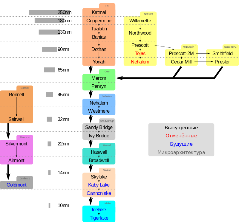 Intel says this node provides a 20% performance-per-watt gain over its predecessor (the same rules above apply) and represents the company’s full embrace of EUV technology. That’s an important step forward — Intel’s laggardly adoption of EUV fabrication is thought to be a major contributing factor to its 10nm delays.
Chips based on the Intel 4 process will debut in 2023, with client Meteor Lake processors coming in the first half and Granite Rapids server products following. That timeline still leaves Intel’s competitors, like TSMC and Samsung, with a process node advantage in the 2023 time frame. TSMC projects it will be in full production of its 3nm node in 2023, explaining Intel’s continued need to outsource some products. Intel plans to leverage its packaging technology and disaggregated design philosophy to integrate externally-produced TSMC chips into its own products to help sidestep the delay.
Intel 3, previously branded as 7+, will bring an 18% performance-per-watt gain over Intel 4 when it shows up in products in the second half of 2023.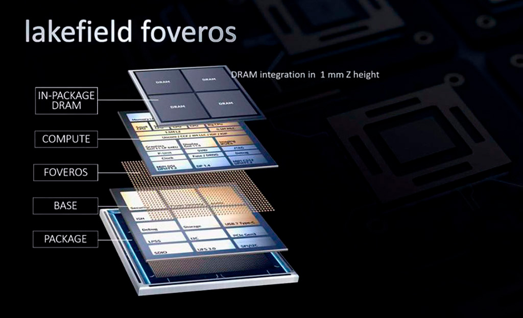 ‘Intel 3’ is an incredibly fast follow to ‘Intel 4’ that launches earlier the same year, due to the previously mentioned delays. Still, Intel has confirmed that, based on its early modeling and test chip data, it represents «a higher level of improvement than a standard full node for Intel — or indeed for other vendors.»
Intel plans to begin an entirely new era in the first half of 2024: The angstrom era. These chips represent the point where some physical features can no longer be accurately measured in nanometers, or billionths of a meter. Instead, these features will now be measured in angstroms, or one ten-billionth of a meter. The first angstrom-class process from Intel will come as 20A (A is for angstrom), which brings RibbonFET, Intel’s first gate-all-around (GAA) transistor, and PowerVia, a novel approach to delivering power to incredibly small transistors.
Intel Angstroms, RibbonFET and PowerVia
Image 1 of 7
Intel Process Roadmap 2021 — 2025 (Image credit: Intel)
Image 1 of 7
Process Roadmap (Image credit: Intel)Image 1 of 7
Process Roadmap (Image credit: Intel)Image 1 of 7
Process Roadmap (Image credit: Intel)Image 1 of 7
Process Roadmap (Image credit: Intel)Image 1 of 7
Process Roadmap (Image credit: Intel)Image 1 of 7
Process Roadmap (Image credit: Intel)Image 1 of 7
RibbonFET will mark Intel’s first gate-all-around (GAA) design and the company’s first new transistor design since FinFET debuted in 2011. Intel’s design features four stacked nanosheets, each surrounded entirely by a gate. Intel claims this design enables faster transistor switching while using the same drive current as multiple fins, but in a smaller area. This certainly seems plausible; Intel’s competitors have also adopted GAA designs.
Intel isn’t sharing much information about RibbonFET yet, but it bears a striking resemblance to IBM’s recently announced GAA/nanosheet tech that it fabbed on a 2nm test wafer (images below). This is incredibly relevant, as Intel recently announced in its IDM 2.0 announcement that it would collaborate with IBM on future logic and packaging technologies. This partnership is important for Intel as it looks to recover from years of stagnation with its process technologies. During our briefings with IBM about its research results, the company was quite clear that its new 2nm tech will benefit all of its partners, including Intel. You can read more about IBM’s similar tech here.
(Image credit: Intel)
As we noted in our coverage of IBM’s nanosheet/GAA tech, the smallest transistors in the world are of no use if you can’t wire them together, and that has been one of the most pressing constraints to shrinking to smaller nodes.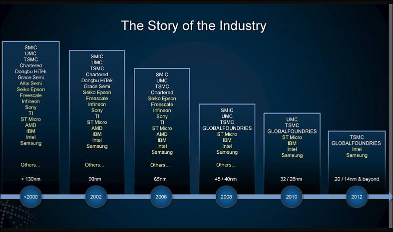
Intel’s new PowerVia technology seems to be a promising approach to navigating the problem with interconnects. PowerVia routes all power for the transistors directly to the transistors through the backside of the transistor. This essentially partitions power delivery to the backside of the transistors while data transmission interconnects remain in their traditional location on the other side.
Intel says that separating the power circuitry and the data-carrying interconnects improves voltage droop characteristics, allowing for faster transistor switching while enabling denser signal routing on the top of the chip. Signaling also benefits because the simplified routing enables the use of faster wires with reduced resistance and capacitance.
This technique will obviously pose many of its own challenges, such as the power delivery circuitry potentially serving as an insulating layer that traps heat within the transistors. It will be interesting to see how Intel tackles those potential pitfalls.
Intel 18A and High NA EUV
(Image credit: Intel)
Intel didn’t include it in the roadmap, but it already has its next-gen angstrom-class process in development. ‘Intel 18A’ is already planned for «early 2025» with enhancements to the RibbonFET transistors.
Intel’s 18A will be the inflection point for using High NA EUV, which is a new ultra-precise version of EUV machines that can etch designs at smaller (<8nm) resolutions than current machines. These machines will be required to do single-patterning EUV at such fine geometries, while existing EUV tools would require less-desirable multi-patterning EUV techniques.
Intel says it will be the first company to receive a High NA EUV machine from ASML, signaling that it plans to lead with the next-gen EUV machines as opposed to lagging behind TSMC as it did with 10nm. It’s noteworthy that while Intel did state that it would be first to receive a High NA EUV machine, it didn’t claim that it would be the first to enter high volume manufacturing with High NA EUV.
Intel tells us that it will offer the leading-edge Intel 3 and the following nodes, including 20A and 18A, to its foundry customers. That means we will likely see Intel stick with offering its prospective foundry customers trailing edge nodes for now — Intel 3 doesn’t enter production until the second half of 2023.
(Image credit: Intel)
Intel’s summary says that the company will achieve process performance parity with the industry leader, TSMC, in 2024, and take the lead in 2025. However, Intel’s footnote specifies that this is based on performance-per-watt, and not transistor performance or density.
It’s noteworthy this parity statement only applies to Intel’s process tech, and not its end products. The company still plans to still compete with «leadership products» from now until 2025 through a combination of new microarchitectures, packaging innovations that tie together various technologies in new and more efficient ways (more on that below), and also by outsourcing some of its highest-end chip designs for the first time in its history. Intel says it will release both consumer and data center «CPU leadership» chips with an as-yet unspecified TSMC node in 2023.
Intel Packaging Update
Image 1 of 9
(Image credit: Intel)
Image 1 of 9
(Image credit: Intel)Image 1 of 9
(Image credit: Intel)Image 1 of 9
(Image credit: Intel)Image 1 of 9
(Image credit: Intel)Image 1 of 9
(Image credit: Intel)Image 1 of 9
(Image credit: Intel)Image 1 of 9
(Image credit: Intel)Image 1 of 9
(Image credit: Intel)Image 1 of 9
Intel’s packaging update was a bit more spartan. The company announced that it would use EMIB packaging tech, which uses an embedded silicon bridge in a package to connect multiple dies, for its Sapphire Rapids processors, marking the first data center product with the interconnect technology. This has been a bit of an open secret, as pictures of Sapphire Rapids have already surfaced. However, Intel did reveal that it will improve next-gen EMIB from a 55-micron bump pitch to 45 microns.
Intel’s Foveros 3D chip stacking technology debuted in the company’s Lakefield processors that the company recently retired, but the next-gen Foveros implementation debuts in Intel’s upcoming Meteor Lake processors. This generation of Foveros improves to a 36-micron bump pitch.
Intel’s upcoming Foveros Omni takes things a step further. This interconnect technology uses copper columns at the peripheries of the interconnected dies to deliver power, while TSV connections throughout the center of the die shuffle data between the chips. This differs from the first-gen Foveros because it separates the data and power transmission, allowing for cleaner routing for both power and data signals. In turn, this enables a tighter 25-micron bump pitch and allows mixing and matching different base dies. This technology is essentially the same as Intel’s ODI packaging tech, which you can read more about here.
Intel has also given its hybrid bonding tech a new use in conjunction with its Foveros packaging. Foveros Direct leverages die-on-wafer hybrid bonding (copper-to-copper) as an alternative to standard thermo-compression bonding. This new technique features aggressive sub-10nm bump pitches that increase interconnect density, simplify interconnect circuitry, and lower resistance and power consumption — all while serving up higher bandwidth. Intel has already taped out a stacked SRAM chip with hybrid bonding, and now the company is applying the technique to its Foveros interconnect. However, Intel hasn’t stated when this tech will come to market.
Intel Renames Process Nodes — Continued
Image 1 of 2
(Image credit: Intel)
Image 1 of 2
(Image credit: Intel)Image 1 of 2
Intel’s decision to rename its process nodes will certainly garner plenty of criticism, but it is a necessary evil. Intel’s process node naming was simple enough back in 1997, when node naming was based on the transistor’s gate length (or M1 half-pitch metric), but the correlation between the physical measurement and the actual name of the node changed over time. In fact, the arrival of FinFET transistors killed the correlation between the two entirely. Now Intel’s node naming changes come with either new technology or increased transistor density.
When it comes to nanometers, everyone knows that a smaller number is better for semiconductors. But while Intel’s naming diverged from a physical measurement slowly, third-party foundries like TSMC and Samsung made more radical adjustments based on even simple changes to the underlying technology. That spurred name changes for situations like the move from planar to FinFET transistors, even when the transition didn’t improve transistor density. Even PDK/BKM (Product Design Kit/Best Known Method) changes are enough of an excuse for third-party fabs to assign a new number to a process, turning the naming convention into more of a marketing exercise than a metric tied to any sort of physical measurement.
And the third-party foundries are winning the marketing wars. However, in the real world, a plethora of factors influence the economics and performance of a process node, such as transistor density, peak performance, performance per watt, different types of logic/circuits, SRAM density, and so on.
Intel’s missteps with its 10nm node, which caused a string of ‘+’ revisions and the delay of three following nodes, exacerbated the node naming issue as Intel ceded its process leadership to TSMC. Now, depending on when TSMC first ships its 3nm process, the company leads Intel by either one or two process nodes. That’s particularly painful for Intel because while its process tech does lag TSMC, its naming lags, too, falsely amplifying the extent of TSMC’s lead. Currently, based on transistor density, Intel’s 10nm is more analogous to TSMC’s 7nm, and Intel’s 7nm is comparable to TSMC’s 5nm, so a naming adjustment makes sense.
Intel also shared some supporting quotes (in the album above) that point to others in the industry pointing out that node naming no longer has any correlation to the actual tech. (One of Intel’s supporting quotes in the slide above says Intel 7nm is close to TSMC 3nm, but take that with a grain of salt.)
It makes sense for Intel to move forward to new naming now that it will compete more directly with TSMC and Samsung in the foundry market, but we’re surprised that it chose to make the move at its 10nm generation instead of waiting for 7nm (which is now called Intel 4). Given that Intel has already shifted from its ‘+’ naming to using full names, like ‘Enhanced SuperFin,’ the new naming adds yet another layer of confusion to interpreting the company’s progress because it is applied to products that are already in flight. Let’s hope Intel sticks to this naming convention, and its roadmap, at least for a while.
Paul Alcorn is the Deputy Managing Editor for Tom’s Hardware US. He writes news and reviews on CPUs, storage and enterprise hardware.
Topics
CPUs
Tom’s Hardware is part of Future US Inc, an international media group and leading digital publisher. Visit our corporate site .
©
Future US, Inc. Full 7th Floor, 130 West 42nd Street,
New York,
NY 10036.
Intel has a new architecture roadmap and a plan to retake its chipmaking crown in 2025
Intel is rethinking how it releases — and brands — its semiconductor innovations, CEO Pat Gelsinger announced today at the company’s Intel Accelerated webcast. The announcement includes the broad strokes of the next half-decade of Intel’s processor roadmap, new chip and packaging technologies, and a promise of an “annual cadence of innovation,” with the ultimate goal of seeing Intel retake its leadership in the processor space by 2025.
Future Intel products (starting as early as its upcoming 12th Gen Alder Lake chips later this year) will no longer use the nanometer-based node nomenclature that both it and the rest of the chipmaking industry has used for years. Instead, Intel is debuting a new naming scheme that it says will provide “a more accurate view of process nodes across the industry” and how Intel’s products fit into that landscape.
Intel rebrands its node naming
How that works in practice is that those new third-generation 10nm chips will be referred to as “Intel 7,” instead of getting some 10nm-based name (like last year’s 10nm SuperFin chips).
At first glance, it sounds a lot like a cheap marketing tactic designed to make Intel’s upcoming 10nm chips look more competitive next to products from AMD, which are already on TSMC’s 7nm node, or Apple’s 5nm M1 chips. And while that’s technically true, it’s not as unfair of a comparison as it necessarily looks. In modern semiconductors, node names don’t actually refer to the size of a transistor on a chip: thanks to advances like 3D packaging technologies and the physical realities of semiconductor design, that hasn’t been the case since 1997 (as noted by ExtremeTech).
And from a technical perspective, Intel’s 10nm chips are broadly on par with “7nm” branded hardware from competitors like TSMC or Samsung, using similar production technologies and offering comparable transistor density. That’s something that translates to commercial hardware, too: we’ve already seen that Intel’s current 10nm chips are still competitive with AMD’s cutting-edge 7nm Ryzen chips, for example.
All that is to say that Intel’s rebranding here isn’t entirely unfair to see, even if it does make it harder to parse when those bigger “node” change advances are happening with the new nomenclature.
Intel’s updated roadmap and node namingImage: Intel
Here’s a look at Intel’s new roadmap and what it all actually means.
• Intel 7 is the new name for what would have been Intel’s third-generation 10nm technology and the successor to Intel’s 10nm SuperFin (aka Intel’s second-generation 10nm chips, found most notably in its 11th Gen Tiger Lake chips). Intel says that the new Intel 7 hardware will offer approximately 10 percent to 15 percent improvements in performance-per-watt compared to the previous generation — or, as is always the case, improved power efficiency and battery life should hardware manufacturers prefer to keep performance the same.
The first Intel 7-based products will show up as early as this year, with the already previewed Alder Lake chips coming at the end of 2021 for consumer products, and the upcoming Sapphire Rapids chips in 2022 for data centers.
• Intel 4 is the architecture formally known as Intel’s 7nm process, which Intel infamously was forced to delay out to 2023 last summer following manufacturing issues. Originally planned for 2021, it’s the next major jump in technology for Intel, using EUV (extreme ultraviolet) technology — something already utilized by Samsung and TSMC’s 5nm node products, for comparison. It’ll still use the same broad FinFET transistor architecture that Intel’s been using since 2011. Thanks to all those improvements, Intel 4 is expected to feature a transistor density of about 200-250 million transistors per mm², compared to about 171.30 million transistors per mm² on TSMC’s current 5nm node.
Intel says that Intel 4 will offer an approximately 20 percent jump in performance-per-watt while cutting down on overall area. Production is set for the second half of 2022, with the first Intel 4 products planned for 2023 (Meteor Lake for consumer products, and Granite Rapids for data center).
• Intel 3, set for manufacturing in the second half of 2023, is the new name for what would have been a second-generation 7nm product under Intel’s previous naming scheme. Like Intel 4, it’s still a FinFET product, although Intel says it’ll offer additional optimizations and use of EUV for roughly an 18 percent increase in performance-per-watt compared to Intel 4. No release date or product names for Intel 3 chips have been announced yet, but presumably, they won’t be available until 2024.
-
Intel 20A is the name for the next generation of Intel technologies that, under the old scheme, would have been the architecture following the formerly branded 7nm node. It’s also the most substantial announcement that Intel made today, technologically speaking, one that will see Intel debut its first new transistor architecture since FinFET in 2011, called “RibbonFET.” The new architecture will mark Intel’s first gate-all-around transistor, a fundamentally new transistor technology for the company that promises greater transistor density and smaller sizes. Additionally, 20A will see the introduction of “PowerVia,” a new technology that allows for wafers to be powered from the back of the chip, instead of requiring power to be rounded to the front.
A closer look at the coming updates for Intel 20A.Image: Intel
The “20A” in the title is meant to evoke the “Ångstrom era” of semiconductor design — an Ångstrom being a unit of measurement smaller than nanometer. (20Å = 2nm, although, like the other rebranded Intel names above, Intel 20A doesn’t refer to a specific measurement on the products themselves.)
Intel’s 20A isn’t expected to ramp until 2024, and, like Intel 3, it doesn’t have any formally announced release date or products yet.
- Intel 18A is the farthest in the future piece of Intel’s roadmap and will feature the second generation of Intel’s RibbotFET technology for “another major jump in transistor performance.” Intel says that Intel 18A is in development for “early 2025,” and that it expects this generation of technology to re-establish its semiconductor leadership.
In addition to all of its process roadmap news, Intel also announced two major updates to its Foveros chip-stacking packaging technologies (the second-generation of which is set to debut in Intel 4’s Meteor Lake in 2023. ) Foveros chip stacking combines several hardware elements into a single die, like Intel’s Lakefield chips, which pile together five CPU cores, an integrated GPU, and DRAM into a compact stack to save internal space compared to a traditional design.
Image: Intel
Foveros Omni will allow for more variety in stacked chips by making it easier to mix-and-match tiles, regardless of their specific size — for example, allowing for a base tile that’s smaller than the top tile in a stack. And Foveros Direct will allow for direct copper-to-copper bonding between components, reducing resistance and decreasing bump pitches. Both of the new Foveros technologies are planned for production in 2023.
Intel’s new names may help the company recontextualize its current and future products more accurately against its competition, but the fact remains that Intel is behind. Even accepting that the Intel 7 is on par with 7nm products from other foundries, those foundries are already past their 7nm chips and on to 5nm hardware. Which means that the companies that rely on those external foundries — like Apple, AMD, Nvidia, Qualcomm, and virtually every other major tech company — can still get chips that are more advanced than Intel’s best work. Apple’s superlative M1 Macs, for example, already use 5nm chips from TSMC — and handily outpace Intel’s comparable products. AMD is rumored to be working on 5nm Zen 4 processors for as early as 2022, too, which could offer similarly concerning competition for Intel from its already encroaching competitor.
Even with the ambitious, annual cadence for its roadmap, Intel is playing from behind; it doesn’t expect to fully catch up to the rest of the industry until Intel 20A in 2024. And it doesn’t expect to reclaim leadership in the semiconductor business until 2025 with Intel 18A. And all that assumes that Intel doesn’t hit any more delays or manufacturing snags like the ones that held up both its 10nm and 7nm processes (which arguably put the company in its current situation in the first place).
After years of setbacks, though, it’s clear that the revitalized Intel isn’t going down without a fight. But the next few years will see whether its efforts are enough.
Intel’s Layout & Process Roadmap to 2025 and Beyond — CNXSoft — Android Set-Top & Embedded News always strictly adheres to its own production schedules for new processes, in particular, its 10nm process suffers from many years of delays.
But the other day, an American company held an event that presented a process roadmap for the period up to 2025 and beyond, which includes 7nm, 4nm, 3nm, and even switching the Angstrom scale (1A = 0.1 nm) with process 20A expected in 2024/2025.
Intel’s Process Roadmap to 2025 and Beyond
Intel’s Historical and Future Processes
As for process nodes, here’s what to expect over the next few years:
- 10-15% and will be featured in Alder Lake for the customer in 2021 and Sapphire Rapids for the data center, with the latter expected to go into production in the first quarter of 2022.
- The Intel 4 promises a 20% increase in performance per watt over Intel 7 and is the first Intel FinFET node to use deep ultraviolet (EUV) lithography, which includes «a highly sophisticated lens and mirror optical system focusing a wavelength of 13 .5 nm for printing incredibly fine details on silicon.” The Intel 4 will be ready for production in H2 2022 with products shipping in 2023, including Meteor Lake for the customer and Granite Rapids for the data center.
- The Intel 3 is expected to provide an 18% increase in performance per watt over Intel 4 and the company will be ready to start manufacturing products based on this technology node in the second half of 2023. Intel has not yet announced which processor families will benefit from the new technology node.
- Intel 20A Coming in 2024 with RibbonFET and PowerVia technologies. RibbonFET is a transistor with universal gate that provides faster switching speeds of
transistors while providing faster switching speeds in a smaller footprint than FinFETs due to its multi-nanochannel structure. PowerVia is the implementation of power delivery on the back of the silicon die, eliminating the need for power routing on the front of the wafer.
 - The Intel 18A is already in development with RibbonFET improvements that will provide another «major leap» in transistor performance in 2025.
Note that there seems to have been a marketing team involved here as Intel 7 used to be called «10nm Enhanced SuperFin» and Intel 4 used to be called «Intel 7nm» technology node. We guess it depends on how you measure it, and Intel has explained in the past that competitors have a different way of measuring transistor size.
Intel
Chassis Innovations Intel also talked about chassis innovations such as the existing Foveros 3D stacking technology found in its ready-to-release Lakefield processors:
- EMIB (Embedded Multi-Chip Interconnect Bridge) in Intel Xeon Sapphire Rapids for Data Centers.
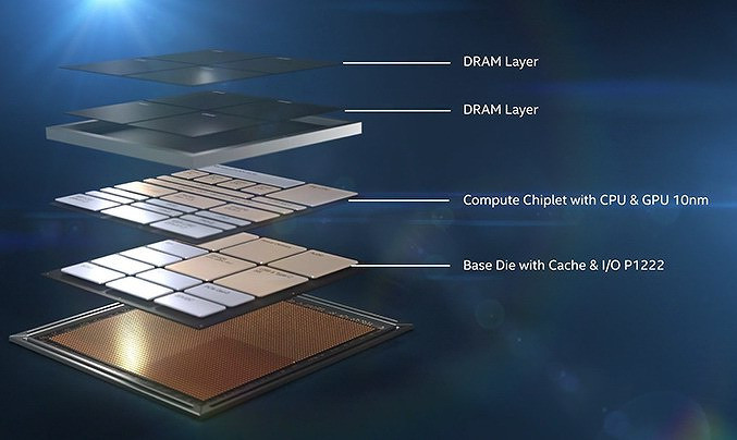 The next generation of EMIB will move from 55 microns to 45 microns.
 - Foveros is not exactly the same as we just noted, but the second generation of 3D stacking technology will be used in Meteor Lake customer products and features a 36 micron ledge pitch, tiles spanning multiple process nodes, and a TDP range of 5 W up to 125 W.
- Foveros Omni is based on Foveros technology, which allows you to connect crystals to each other in several layers of conductors at once. Mass production of processors based on Foveros Omni should begin in 2023.
- Foveros Direct will be free for Foveros Omni and will be available around the same time. It is based on a direct copper-to-copper connection for low-resistance inter-chip connections and provides a pitch of no more than 10 microns, providing an order of magnitude increase in interconnect density for a 3D stack.
More information can be found on the Intel website, as well as on the Anandtech website, which compares new Intel processors with TSMC processes, Samsung or even IBM, etc.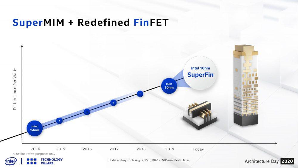
We express our gratitude to the source from which and the article was translated to cnx-software.com.
You can read the original article here
CategoriesIntel, Hardware, ProcessorsTagsAlder Lake, FOVEROS, Intel, processor
News on the topic «Intel introduced a technological roadmap until 2025» — NVIDIA WORLD
Intel clearly needed to do something with the name of technological processes. For years we have seen 14nm technology with endless benefits, now we see 10nm and the newly introduced 10nm Enhanced SuperFin.
IBM announced another technological milestone by introducing the world’s first 2nm chip.
As you might expect, the new technology will provide many of the energy efficiency and performance benefits that come with migration to new, thinner process technologies.
IBM’s 2nm processor can accommodate up to 50 billion transistors and delivers 45% more performance and 75% less power than today’s 7nm chips.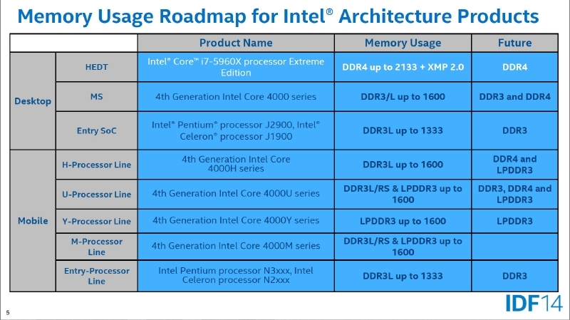
IBM
experimental 2 nm processors The main advantages of 2 nm technology are named by IBM itself:
- Extending the battery life of smartphones by 4 times, charging will be required every 4 days.
- Reducing the carbon footprint of data centers that consume 1% of the world’s energy. Equipping these servers with 2 nm chips will significantly reduce this value.
- Dramatically speed up laptop performance, from faster application processing to language translations and faster Internet connectivity.
- Faster object detection and response in self-driving car systems.
It is noteworthy that earlier IBM was also the first in the world to introduce 7 nm and 5 nm technologies. Thus, the company continued its leadership trend with the 2nm process.
technologiesproduction2 nmchips processorsIBM
comment on related news
KitGuru
This means that the first 7nm processors will appear only in 2022. The company’s transition to 10nm technology is not a success. CFO George Davis notes that the 10 nm technology used to manufacture Ice Lake processors is far from the best. It has » less productivity than 14nm, less productivity than 22nm. It won’t be the robust technology that people expected versus 14nm, or what they’ll see in 7nm» .
Intel
The problem is that Intel can’t raise the frequencies, and the pancake yield is lower than the 14nm process. Ice Lake processors compete with 14 nm Comet Lake processors, and only have advantages in graphics.
Now the company plans to become more aggressive. She has been using third-party production for system logic for several years.
Now CEO Bob Swan is looking for a more «pragmatic» approach to using third parties. This means that the company will order more critical components from third parties, such as GPUs or even CPUs.
10nm Intel Alder Lake desktop processors will hit the market in the second half of 2021.
production 7nmIntel processors
comment related news
Given that the company’s new flagship Core i9 processors-9900K, Core i7-9700K and Core i5-9600K, will be released on October 8, Intel saw no other way than to open another production site in Vietnam.
Intel Core i9 Processor
The company’s press release states: “In order to ensure continued supply of processors…Intel will add additional manufacturing facilities for developmental/finished goods. The new zone is located in Vietnam. The new production area has become a certified equivalent (in form, size, function and reliability) to the company’s products and technologies” .
production 14 nm Core i9 Intel processors
comment on related news
TweakTown
The cost of creating microcircuits less than 10 nm is relatively high. HiSilicon recently planned to spend at least $300 million to develop next-generation 7nm SoC. Developers, deprived of production, are afraid to spend big money on sub-10 nm processes, doubting that these costs will pay off in the future.
Qualcomm Snapdragon
For example, Qualcomm and MediaTek, instead of developing 7nm SoCs, decided to upgrade their mid-top solutions, which will be released on a 14/12nm process. Both companies are wondering if there is a need to move to 7nm manufacturing.
As for the manufacturers themselves, TSMC and Samsung Electronics have already presented roadmaps with 7nm chips. UMC decided to shift the focus to mature and specialized processes. Approximately along the same path, they decided to move to GlobalFoundries, closing their 7nm program. The largest chip manufacturer, Intel, is completely bogged down in 14nm technology, already 3 years late with the 10nm process.
UTB technology uses lower forward and operating voltage and provides better energy savings. In addition, it requires lower operating costs than FinFET. It should be noted that not only the Chinese HH Grace Semiconductor is interested in the technology, but also Globalfoundries, Samsung and STMicroelectronics.
The total revenue in the UTB camp will be less than that reported by TSMC, but UTB manufacturers have fewer orders for mid to low priced chips and cannot match the FinFET process sales volumes, setting clear targets for UTB.
Analysts also note that chip vendors producing expensive, high-performance chips want to fabricate their processors in FinFET factories.
technologiesproductionprocessors
comment related news
Fudzilla
Last November, Intel CEO Brian Krzanich said he wanted to expand Intel’s contract manufacturing business, which should increase the company’s profits.
The company recently announced that it had secured a major customer for this business, and now it will produce processors for the company’s audio and visual equipment with Panasonic’s LSI.
Panasonic’s LSI division manufactures video encoding and decoding chips for all Panasonic home media products, from TVs to audio receivers and Blu-ray players. The chips themselves will be designed by Panasonic and then manufactured by Intel using a 14nm process.
Although Intel has a number of other customers for its manufacturing facilities, such as Altera, these customers were only for FPGA (Field Programmable Gate Array). Panasonic will be the first customer for processors. This means that the company is entering a market dominated by Taiwan Semiconductor Manufacturing Corporation (TSMC) and GlobalFoundries. And while Intel is trying to catch up with these companies in terms of contract manufacturing, it will be interesting to see if 14nm becomes competitive enough to attract more customers.
production 14nm processors IntelPanasonic
comment related news A new high-performance line of CPUs will replace the Ivy Bridge-E, while the new generation chips will cost about $1,000.
New processors will also require special X9 series chipsets9, which will also be released at the same time. However, these processors will make up a small fraction of the total processors.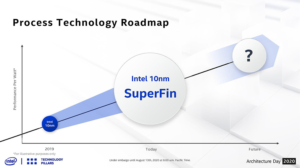 So, by the end of this year, the total share of Ivy Bridge-E and Haswell-E processors will be less than 5% of the total Intel CPUs that the company plans to ship in 2014.
As you know, the Haswell-E series will use a 22 nm process technology, while it will have two parallel lines — X and K. The processors will support Hyper-Threading and Turbo Boost 2.0 technologies, PCI-Express Gen 3.0 and DDR4 memory with a frequency of up to 2133 MHz .
The chipset will add built-in support for USB 3.0 ports and 10 SATA ports with a bandwidth of 6 Gb / s.
Intel will release the Haswell Refresh platform this spring, with an official launch at Computex 2014 in June.
ForecastProductionHaswell-E Intel processors
1 comment .
2.3GHz is currently the frequency limit for the 28nm Snapdragon 800 and Tegra 4i (Grey), which will be released later this year or early next year.
And as usual, to overcome this limitation, it is necessary to use a process with a smaller size of transistors. TSMC’s 20nm process will provide a 30% increase in speed and a 1.9x increase in density with a 25% reduction in power consumption. A 30% boost means that the SoCARM frequency will be at 3 GHz with a significant increase in the number of transistors used mainly for the needs of the GPU. Most likely, this is how NVIDIA will ensure the installation of the Kepler video core in the Logan processor, but so far there is no confirmation of this.
A 25% reduction in power consumption would mean a quarter longer battery life, and since short battery life is a major disadvantage of smartphones, this modification will be extremely important for consumers.
This technological transition will significantly improve the position of the ARM alliance in competition with manufacturers of x86 processors. But do not forget that Intel and AMD are not asleep. In 2014, Intel is planning to release its 14nm Atom for tablets and smartphones, while AMD is also planning to release its 14nm chips for tablets and laptops with GlobalFoundries manufacturing support.
production14 NM20 NMARMSOCOCOCECESEMDGLOBALOBALFUNDRESISMC
Comment similar news
FUDZILLA
Intel conducted a good technical press conference, in the course of the company Mark Bork BOH) .
He said that Intel hopes to have 14nm production by the end of 2013. This process will be on schedule for the next generation of processors, codenamed Broadwell, which will go into mass production in 2014.
The process itself is called P1272 and involves the use of circuit elements equal to 16 nm, however, Intel has taken some steps that made it possible to compact the crystal elements. The developers managed to arrange the elements more densely than expected 6 years ago, when this process technology was just announced. As a result, Intel has a more energy-efficient roadmap, as opposed to its earlier performance-focused roadmap.
Talking about the company’s future, 10nm technology research is planned for 2015. At the same time, Intel is working on both 7nm and even 5nm process technologies, but Bohr did not specify the expected timeline for their entry into production.
If Intel continues to update the process technology at the same pace, then if 10nm lithography is released in 2015, 7nm will appear in 2017, and 5nm technology in 2019.
technology interview5nm7nm10nm14nmBroadwellIntel processors
comment on related news
In this conversation, our colleagues discussed with Bleemer the technological prospects for the company’s development after the transition to 22 nm technology standards, which will be used in the Ivy Bridge family of central processors. Unfortunately, Bleemer did not focus on the technical details of the issue, and did not even indicate the approximate date when new technological solutions would appear. However, he noted that they will make full use of the three-dimensional transistor Tri-Gate technology, the same as in Ivy Bridge, and that the test circuit of the future technology is already operational.
“We need to keep going and you can trust me that we already have a working next generation after 22nm in our labs, so we need to keep going… I really can’t say more about this than that in the lab we are already on the way, our engineers are already on the way to launch and manufacture 14nm products… And I think our most important achievement was the metal 3 D gates, and only the design of the gates, in fact, can provide more efficient use of energy and less heat generation” .
We would like to remind you that in summer the company announced further production plans. Then, 14 nm process technology was planned for implementation in 2014, and 10 nm — around 2018.
interviewtechnologies14nm22nmIntel processors
comment on related news
Nordic Hardware
On Tuesday, we reported that AMD is phasing out the legacy Phenom II and Athlon II processors. Now, Intel has taken similar actions on its part, announcing the phasing out of obsolete chips for LGA775 and LGA1156.
End-of-life CPUs include Core i5-661, i3-530 for LGA1156 and Pentium E5700, Celeron E3500 and E3400 installed in LGA775.
The Core i5-661 and Core i3-530 processors will be available for order until April 27, 2012, and their tray versions will end on October 5, 2012. Box versions of these chips will ship until stocks last.
Orders for the Pentium E5700 and Celeron E3500 will end on December 30 this year, and the company plans to stop deliveries on June 8, 2012 for tray processors, and similarly to older models, these boxed versions can be purchased until stocks are exhausted in warehouses.
MarketProductionCPUIntel processors
Comment on related news
Tech Connect Magazine 2015.
For example, Intel currently manufactures its processors using 32 nm technology. 22 nm chips should appear already this year, however, most likely, the release of these chips will be delayed.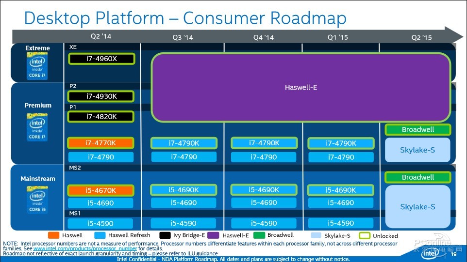 According to Intel’s current technology roadmap, 14nm chip production will begin in 2013, with the company planning to move to 10nm in 2015. Next week, IDF will be held in San Francisco, where Intel will present an updated roadmap. I wonder if the existing deadlines will be shifted?
At the same time, GlobalFoundries plans to transition to 20nm in low-power ICs for networking, wireless and mobile devices only in 2013. At the same time, the company plans to start producing high-power processors using a 20 nm process technology in 2014. This data is fully consistent with AMD’s plans for the transition to new technical processes, which allows us to consider this information plausible.
In addition to reducing the size of integrated circuits, Chian also suggested that in 2015 their production will switch to the use of wafer pancakes with a diameter of 450 mm.
However, none of the three companies announced the use of SOI (silicon-on-insulator) technology in their future chips.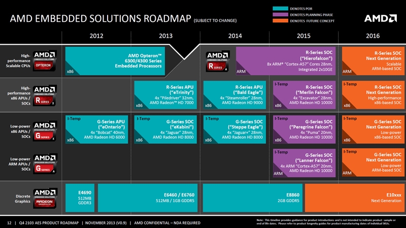 However, this does not mean at all that the entire top three have abandoned this. However, according to rumors, Samsung will be the first to switch to 14nm SOI technology using wafers with a diameter of 450mm.
process technology14 nm20 nmprocessorsGlobalFoundriesIntelSamsungTSMC
comment on similar news
Bright Side Of News
Processor giant Taiwan Semiconductor Manufacturing Co. (TSMC) may be the first to introduce ICs with 3D transistor coupling. Moreover, this may happen as early as the end of 2011. At the same time, they will be able to bypass the semiconductor giant — Intel.
This report was prepared the day before yesterday by the Taiwan Trade Group. The report is based on unnamed sources. Intel introduced its 3D transistor technology in May of this year, at the same time TSMC stated that they were not interested in such technical processes, and that all their efforts were aimed at reducing the physical size of transistors.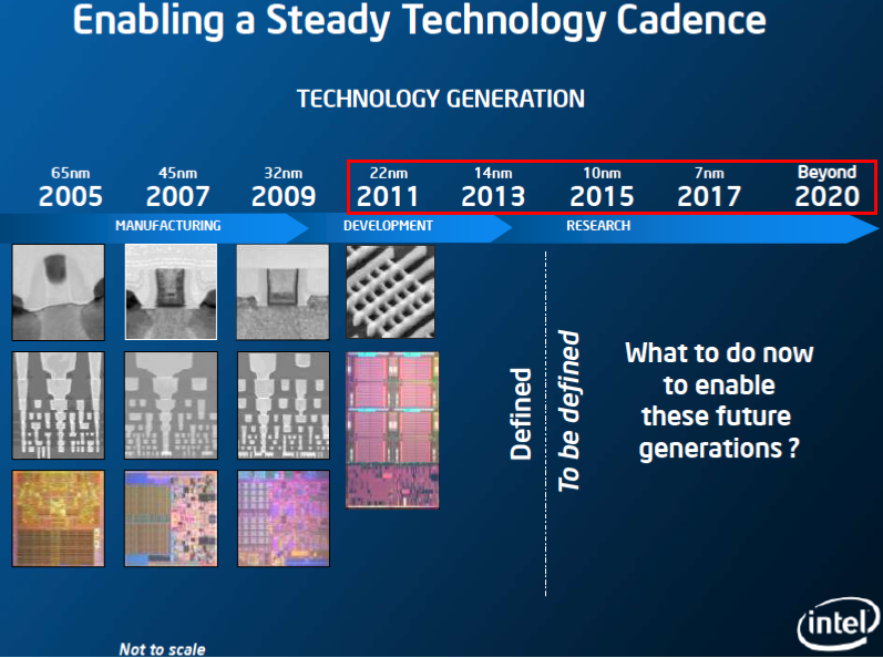 However, it is unlikely that it will be possible to catch the company’s management in a lie, because there are fundamental differences between the developments of Intel and TSMC.
So, the technology of Taiwanese developers, called (Through Silicon Vias — TSVs), is a multilayer microcircuit, in which there are interconnections between the various layers that pass through. In Intel’s Tri-gate design, the silicon traces protrude from the semiconductor substrate.
According to a TAITRA report, TSMC’s 3D technologies will greatly increase the density of transistors in a chip, up to 1000 times. Devices with 3D chips will consume 50% less electricity. The new technology will bypass many of the difficulties created by the traditional «flat» chip technology.
TSMC Senior Vice President of Research and Development Shang-Yi Chian confirmed the information in the report and said that their company is now actively cooperating with chip developers to commercialize 3D manufacturing technology.
technology workflow manufacturing Intel TSMC
comment on related news
EE Times
Intel’s next-generation processors, codenamed Westmere-EX, may have more cores than current server processors. On Sunday it was reported that Intel is preparing a paper titled «Westmere-EX: A 20 Thread Server CPU» for the «Hot Chips 22» conference to be held at Stanford University in Palo Alto, California between August 22 and 24 of this of the year.
There are currently processors with 16 threads that some Nehalem-EX processors have with eight cores. The Westmere-EX processors are a further development of the Nehalem-EX processors, capable of running two threads simultaneously on a single physical core. Intel already offers chips based on the Westmere architecture for laptops, desktops and servers that can run two threads per core at the same time. Therefore, the ability to run 20 threads indicates that Westmere-EX processors will have possibly up to 10 physical cores.
Intel has previously stated that Westmere-EX chips will have more cores and run at higher speeds than Nehalem-EX, although it has not provided further details.
Intel also stated that Westmere-EX will be designed for servers with four or more sockets. The chips will be produced using a 32nm manufacturing process and will be released next year.
In addition, there are rumors that IBM and Advanced Micro Devices will present their server chips at the conference. IBM will be talking about the next generation «System z microprocessor». AMD will also be talking about its next generation of desktop and server processors codenamed «Bulldozer» and «Bobcat» microarchitectures for thin and light laptops and other low-power devices. 9
RumorsTechnologiesAMDIBMIntel processors
comment on related news
Guru of 3D insulating property.
As you know, the first chips made according to 32-nm production standards are processors with the Westmere architecture, which provides for the integration of a 45-nm video core and two 32-nm x86 computing cores into one package. This approach largely changes the existing scheme of interaction between the system logic set and the central processor and should provide higher performance for integrated graphics.
Processors will be designed for the recently released LGA-1156 header and P55 chipset. However, the video core built into Westmere will require a new set of system logic — the H55 / H57 chipset, which will have a bus for interacting with the graphics accelerator, because the controller responsible for the video output still remains on the motherboard.
Westmere architecture will be available for both desktop and notebook processors. The former were codenamed Clarkdale, while the latter were codenamed Arrandale. The desktop solutions will be sold under the Core i5 600, Core i3 500 and Pentium G names and will be available for purchase early next year. Mobile processors will appear on the market at the end of this year.
technologyWestmereIntel processors
comment on related news
TechPowerUp
40 years of experience in the production of central processor units allows Intel to currently hold more than 80% of this market. AMD almost single-handedly opposes the almighty giant and, despite solutions that are quite comparable in quality, it occupies only a small part of the market.
However, the CPU industry will have another strong point in the future. 7 major chipmakers based in Japan team up to create an alternative to Intel. An alliance of Hitachi, Toshiba, Fujitsu, NEC, Renesas, Panasonic and Canon is working on a new processor that will use the energy-saving efforts of Professor Hironori Kasarahara of Washid University. The ultimate goal is to create a processor that would operate on a small charge of solar panels.
The chip must be completed in 2012. So for now, it’s premature to talk about a serious confrontation with Intel.
technologiesIntel processors
ExpReview
One of the reviewers and collectors with the nickname YuuKi-AnS posted photos of a smaller Cannon Lake-Y processor than the only released12 Core i3-8 model.
This series was introduced in 2018 and was withdrawn from sale two years later, making it the shortest running model.
Unknown Intel Cannon Lake-Y
Processor The newly discovered chip is built on three cores, which makes it noticeably different from the traditional dual-core version. The third core is reported to be McIVR, which has an area of 13.72 mm 2 . It is known that this is not a special test piece, but it is clear that glued thermocouples are necessary for testing.
Unknown Cannon Lake-Y processor specifications
The Cannon Lake series was only available with two Palm Cove cores and was offered exclusively with the Crimson Canyon NUC and some low-end laptops. The engineering board is clearly not made for the NUC Mini-PC, and such a small CPU in the center looks very unusual. At the same time, all the connectors shown in the photo were used for validation at Intel.
Motherboard with Cannon Lake-Y processor. Top side Cannon Lake-Y processor motherboard. Downside
Intel Cannon Lake processors are no longer supported. Last year, Intel removed the graphics driver for this series of processors because no processors in the series were released with integrated graphics.
Cannon LakeCPUIntel processors
comment on related news
Several sources have published a table with data on the 13th generation of 13th generation Core processors, including four Core i9 models, four Core i7, five Core i5 and one Core i3. The line includes both models with K and without K, both with the F index, without a GPU, and without it. All K and KF chips have a TDP of 125W, while regular chips with a locked multiplier have a TDP of 65W.
Intel Raptor Lake
processor specifications Traditionally, non-K versions have lower operating frequencies than those with K. Core i9 processor versionshave a formula of 8 + 16 cores, Core i7 — 8 + 8, Core i5 — 6 + 8. Separately, there is a Core i5-13400 model with 6 + 4 cores. The Core i3-13100 processor has only 4 P-cores.
RumorsRaptor LakeCPUsIntel processors
comment on similar news
The Core i7-13700K chip took part in the tests. In the first test, the chip worked on 8 productive cores (P-cores or Performance cores ) clocked at 6 GHz. Hybrid mode was disabled, meaning efficient cores (E-cores or Efficient cores ) didn’t work. In this case, in single-core mode, the chip showed 983 points, which is even higher than the Core i9-13900K at 5.5 GHz with P-cores enabled.
Core i7-13700K @ 6GHz
In the multi-core test, the processor scored 7814 points. In this case, the voltage was 1.421 V, and the temperature was in the range from 25 to 37 ° C.
Core i7-13700K Test at 5.8GHz
In another test, the processor ran all 16 cores, but reached 5.8GHz for P-cores and 3.7GHz for E-cores. In this case, the chip scored 947 points in the single-core test, and 12896 in the multi-core test. The temperature was slightly higher, from 28 to 38 ° C, and the voltage was 1. 5 V.
5 V.
faster than the 5.5GHz i9-13900K and 16% faster than the 5.2GHz Core i9-12900K.
Intel 9 CPUs0007
comment related news
Videocardz
AMD will release Zen 4 processors in the second half of the year. They promise great performance, but Intel isn’t sitting idle either. The company is preparing Raptor Lake processors, which will put serious pressure on the competitor.
The Guru of 3D website published fresh rumors about Raptor Lake processors, according to which their performance, in relation to the current Alder Lake, will increase by 8-15% per core due to changes in the architecture. In a multi-core scenario, there will be a performance gain of 30%-40% due to both architecture changes and an increase in the number of cores, which is a significant technological increase within a single generation. The processors are expected to arrive in the third quarter of this year, shortly after Zen 4 hits the market.
Intel Raptor Lake
processor Intel recently confirmed that Raptor Lake processors will feature up to 24 cores and 32 threads, compared to Alder Lake’s 16 cores and 24 threads, so such a high performance jump seems to be justified. At the same time, AMD Zen 4 will have the same number of cores as Zen 3, but the architecture will be changed very much, and the processors will have a much larger thermal package and will be able to operate at frequencies above 5 GHz, which means that to By the end of the year, another battle of processors awaits us, which, of course, plays into the hands of us, consumers.
RumorsRaptor LakeCPUsIntel processors
Comment Related news
These will be the simplest processor models in the family, since they will contain only “small” Gracemont cores, without Golden Cove, unlike their older counterparts. Another oddity is the complete absence of PCIe lanes from the processor. All peripherals will be connected exclusively to the chipset.
Most likely Intel will use these processors for embedded solutions. The older model should have 8 Alder Lake-N cores. Given the absence of PCIe lanes from the processor, their number will be very limited, since the chipset will provide only 9. Obviously, only an embedded system will be able to successfully work in such a configuration.
It is possible that the new SoC will be used by Intel in Chromebooks or budget laptops, but they will have to be sold at a minimum price to compete with Chromebooks.
Expected Alder Lake-N Specifications
Alder Lake-N processors are also said to feature full GT1 Gen 12.2 graphics with 32 execution units, giving graphics performance comparable to desktop CPUs. However, most likely, the clock speed of these GPUs will be significantly reduced.
RumorsAlder LakeLake-NCPUIntel processors
Comment on similar news
The company is currently partnering with Green Revolution Cooling to develop a testing framework with similar cooling for various Intel data center customers. The very same company Green Revolution Cooling, or GRC, specializes in the development of immersion cooling systems and other similar solutions for data centers.
Xeon Scalable
Immersion cooling completely submerges components in a dielectric thermal fluid to cool the hardware components. The manufacturer also said that ongoing research with Intel also helps to test such solutions and their effectiveness. Right now, Xeon Scalable processors are being used to test the process.
Example of an immersive cooling system
Data center customers will be happy to adopt this type of cooling as it can improve the overall energy efficiency of systems. High performance computers, servers among others, continue to get denser, with more and more cores, so keeping them cool becomes a challenge.
CPUXeon processors server cooling systems Intel
comment on similar news
Neowin
Intel Alder Lake processors will be replaced by new Raptor Lake processors next year, and they will have some improvements over the current generation.
One of their features will be the presence of a digital linear voltage regulator (Digital Linear Voltage Regulator — DLVR). The idea of using it is to use the regulator built into the processor in parallel with the traditional main regulator located on the motherboard, which should reduce power consumption. This will be a relatively cheap solution with low configuration complexity.
Intel Raptor Lake
Processor According to available information, DLVR can reduce CPU power consumption by 20-25%. On the other hand, this means that a 21% reduction in voltage can be translated as a 7% increase in performance.
Thus, the 13th generation of Core processors called Raptor Lake (designed for desktop and mobile devices) will not only increase the number of cores (up to 16 effective), but also offer increased cache, support for LPDDR5X memory, as well as lower power consumption or performance gain due to digital linear voltage regulator. Some of these features will require motherboard upgrades to 700-series chipsets.
Raptor LakeCPUprocessorspower supplyIntel
comment on similar news
Dark Vision Hardware
For an additional fee of $ 50, it was proposed to programmatically improve the functionality by increasing the cache by 1 MB and enabling Hyper-Threading. It seems that now Intel is preparing a similar solution, but for Xeon processors.
Phoronix has exposed a Linux patch on GitHub for a feature called Intel Software Defined Silicon or SDSi. This feature is for Xeon processors, and the SDSi page says it «provides configuration of additional CPU features through the license activation process» .
Intel Xeon
Phoronix also notes that «the SDSi kernel driver exposes a per-socket interface so that its user application can obtain an authentication key certificate stored in the internal NVRAM» , receiving «paid activation option» . What exactly Intel offers to do for an additional fee is not yet entirely clear. But given the previous experience of Intel, we can assume that we are talking about support for instructions, for example, AVX-512, or even additional processor cores.
Intel Xeon processors
comment on related news But it turned out that this does not mean the market availability of the entire model range.
Alder Lake enthusiast variants, top models such as the Core i9-12900K, i7-12700K and i5-12600K, along with high-end motherboards with Z690 chipsets, will be the first to hit the market, according to the latest information. There should also be variants of KF processors in which the graphics core will be disabled.
Intel Alder Lake
Processor Architecture As for the locked multiplier processors without the letter K in the name, they will debut next year at CES. Mid-range and low-end chipsets will also be available at a later date. This information is somewhat consistent with recent rumors that Alder Lake processors will not appear this year. Now it becomes clear that for the mass consumer they really will not be available yet.
In addition to information about the release date, information about support for DDR5 memory on new platforms is also reported. It is noted that DDR5 memory is reserved exclusively for the Z690 and W680 chipsets, and owners of boards based on the B660 and other entry-level chipsets will remain with DDR4.
Alder LakeCPU processors Intel
comment on related news The most interesting from the Intel Accelerated conference — AIN.UA
July 27, 2021,
10:12
685
Intel held an Intel Accelerated conference, where it shared its processor roadmap for the next 5 years, the company’s plans to rename technical processes and named the first customers for whom Intel will make chips.
As noted by The Verge, the main goal that the company set for itself during the conference is to return Intel to leadership in the development and production of processors by 2025.
Naming is no longer tied to process technology
Image: Intel
Future Intel products (starting with upcoming 12th Gen Alder Lake chips later this year) will no longer use the nanometer-based node nomenclature that Intel like all other manufacturers have been using for many years.
Instead, Intel introduced a new naming scheme that the company says will provide «a more accurate representation of technology nodes in the industry.» And according to the new naming, the 3rd generation 10nm chips will be called «Intel 7», instead of getting some name based on the number 10 (like last year’s 10nm SuperFin chips).
At first glance, the decision to drop the process name looks like a marketing ploy and an attempt to make the upcoming 10nm Intel chips more competitive compared to AMD products that are already manufactured using TSMC’s 7nm technology, or Apple’s 5nm M1 chips .
But in practice things are not so simple. There is simply no single process measurement standard for all vendors in the world that would make it possible to unambiguously evaluate a chip as a representative of a particular generation. Moreover, in modern semiconductors, the names of the process technology no longer actually refer to the size of the transistor on the chip.
And from a technical standpoint, 10nm chips from Intel are generally on par with «7nm» chips from competitors like TSMC or Samsung and use similar manufacturing techniques and offer comparable transistor density. This means that Intel’s rebranding isn’t entirely unfair here, even if it does make it harder to tell which process technology it’s talking about.
Intel
roadmap Image: Intel
According to the processor manufacturing roadmap, architectures that should «conquer» the market for Intel are waiting for us in the near future. For the most part, these are renamed technical processes that users have already been waiting for, but there are also loud statements, such as the transition to a fundamentally new architecture sometime in 2024. In general, the Intel Roadmap for the coming years is as follows:
Intel 7 is the new name for Intel’s third-generation 10nm technology and the successor to Intel’s 10nm SuperFin technology. Intel says the new Intel 7 hardware will offer an estimated 10 to 15 percent improvement in performance per watt over the previous generation.
The first Intel 7-based products will arrive this year, with the already announced Alder Lake chips coming in late 2021 for consumer products, and the upcoming Sapphire Rapids chips in 2022 for data centers.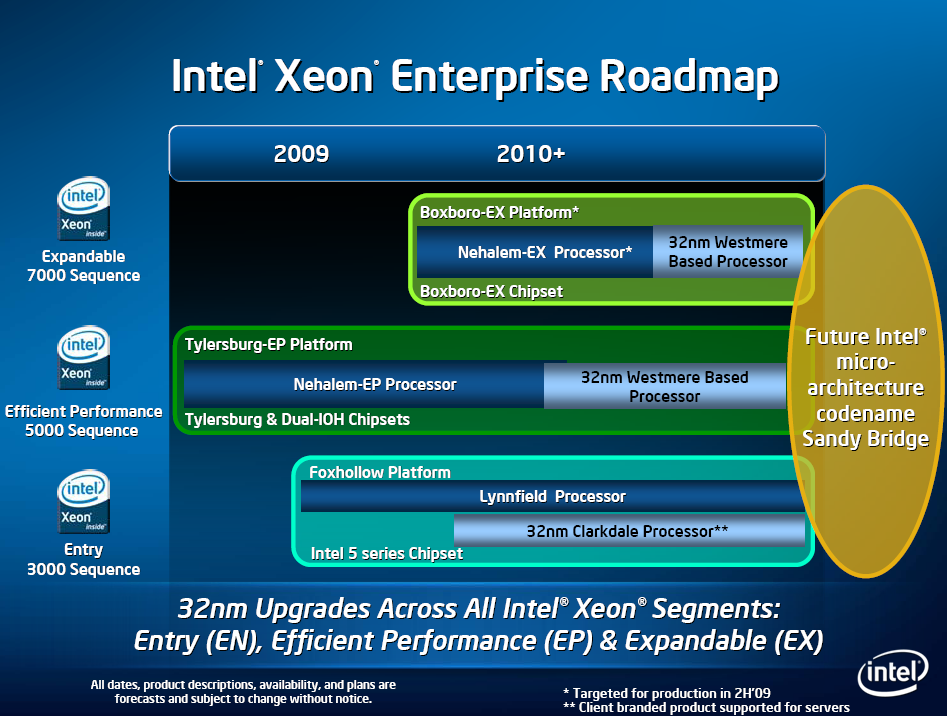
Intel 4 is an architecture that is actually Intel’s 7nm process that the company was forced to delay until 2023 due to manufacturing issues.
Intel says the Intel 4 will offer roughly a 20 percent jump in performance per watt in a smaller footprint. Production is scheduled for the second half of 2022, with the first Intel 4 products scheduled for 2023 (Meteor Lake for consumer products and Granite Rapids for data centers).
The Intel 3 , scheduled for production in the second half of 2023, is the new name for what would previously have been a second generation 7nm product. Like the Intel 4, it’s still a FinFET-based product, although Intel says it will offer additional optimizations and use of EUV to increase performance by about 18 percent over the Intel 4. No release dates or processor names for this architecture have been announced by Intel.
Image: Intel
Intel 20A is the name of the next generation of Intel technologies, which under the old scheme would have been the architecture following 7nm.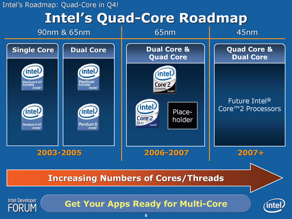 This is also the most significant announcement made by Intel at this conference, as Intel plans to unveil its first new transistor architecture since FinFET in 2011 for the first time. The new architecture, called «RibbonFET», will be a groundbreaking transistor technology for the company, and promises greater transistor density and smaller size.
The Intel 20A is not expected to hit the market until 2024 and, like the Intel 3, it does not yet have an officially announced release date or products.
Intel 18A is the furthest of Intel’s future plans. The Intel 18A will use second-generation Intel RibbotFET technology, marking «another significant leap in transistor performance.» Intel expects this generation to return the company’s leadership in semiconductors.
AWS Amazon and Qualcomm become Intel 9 customers0014 Image: Intel
In addition to the roadmap and process renaming, Intel announced that it has received its first major customer from its new Intel Foundry Services (IFS) contract manufacturing business.
Qualcomm, best known for its development of the Snapdragon chips that power most mainstream Android phones, will begin manufacturing its Intel chips using the upcoming 20A process in the coming years. It has not yet been announced when the first Intel-made Qualcomm chips will appear and what Qualcomm products will be manufactured by Intel.
In addition, Amazon’s AWS will work with Intel Foundry Services, relying on Intel’s packaging solutions (although Intel will not directly manufacture chips for Amazon).
Intel explains why it makes 14nm processors while AMD masters 5nm
Technology
|
Share
In 2021, Intel will release almost all of its processors using the old 14nm topology. She is in no hurry with a full transition to 10 nm, since this technical process pumps money out of her, while 14 nm has long paid off and makes a profit. Meanwhile, AMD is already working on 5nm chips.
It’s all about the money
Head of Intel Robert Swan (Robert Swan) has officially confirmed its dependence on obsolete 14-nanometer process technology. He said that Intel would rely on him for at least another year. Meanwhile, AMD, Intel’s main competitor in the processor segment, has begun preparations for the transition to 5 nm.
As part of Intel’s quarterly reporting conference, Robert Swan said that the company directly benefits from the 14-nanometer process technology, since it allows the company to reduce its costs for the production of chips (Intel, unlike AMD, has its own factories). Swan emphasized that the equipment for the production of chips according to 14nm standards has long paid off, unlike 10nm, which Intel has been trying to switch to since August 2019.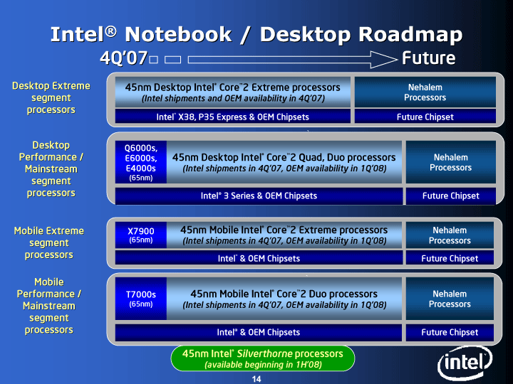
From 10 nm one damage
Robert Swan made 10nm the «big villain» after reporting minimal costs for chip production using 14nm technology. According to him, the new production lines have not yet paid back all the investments.
Robert Swan believes in 14nm, but Intel’s financial results say otherwise
Swan added that Intel’s operating profit now directly depends on 10 nm. He said that the company is now accelerating the pace of transition to new norms, which is negatively affecting the growth of operating profit.
The ability of 14nm to make money for Intel has led to the fact that most of the processors that it intends to produce in 2021 will be released according to these standards. Robert Swan did not name the exact percentages.
Intel’s troubles with the move to 10nm are somewhat similar to the difficulties the company faced with rolling out 14nm manufacturing. According to its plans, it was supposed to start mass production of such chips at the end of 2013 — the beginning of 2014, but in the end everything had to be shifted a year ahead. Thus, Intel has been distributing 14nm chips since Q1 2015.
Intel is going to accelerate
Despite its reliance on 14nm, Intel is not giving up on the full transition to 10nm. As CNews reported, in early October 2020, she finally launched her 10-nanometer Fab 42 plant in Arizona (USA), which took her almost 10 years to build.
The new fab is designed to produce 2nd and 3rd generation 10nm products, the hottest for Intel as of October 2020. 2nd generation includes Ice Lake-U, Ice Lake-SP, Elkhart Lake, and Snow Ridge processors, while 3rd generation is they are Tiger Lake-U and Tiger Lake-H debuting in September 2020.
One of the first Intel Tiger Lake
processors
At the reporting conference, Robert Swan, who has been managing Intel since February 2019, did not ignore the company’s problems with the ultra-modern (for it) 7-nanometer process technology. Back in July 2020, the company officially admitted that its new chips with 7 nm standards would not be available for at least another two or three years. This was immediately followed by the dismissal of the head of the key technology division of Intel Merty Renduchintala (Murthy Renduchintala) from the company, and on July 24, 2020, due to a delay in the new technical process, the value of Intel shares collapsed by more than 10%
Speaking about the problems with 7 nm, Robert Swan said at the time that the problem that prevents his company from mastering the new norms had already been found, and that Intel specialists were working on fixing it. Now Swan reported on her elimination. “We have fixed everything and made wonderful progress” (we’ve deployed the fix and made wonderful progress), — said the head of the company.
Anton Smirnov, AI Cloud: AI magic begins where servers are combined into “teams”
Artificial intelligence
What exactly the problem was, and how Intel dealt with it, Swan did not specify either in the summer of 2020 or now. He also did not set new release dates for the first 7nm chips, so they are still expected no earlier than 2022, or even 2023.
Financial position of Intel
Robert Swan spoke about all the nuances with technical processes at a conference on Intel’s financial report for the third quarter of 2020. This period for Intel ended with a 4% drop in revenue year-on-year to $18.3 billion. The profit margin decreased by 5.7 percentage points — up to 53.1%.
The company’s operating profit also decreased, moreover, by 22% at once, falling to $5.1 billion, while net profit showed an even more rapid drop compared to the third quarter of 2019. It decreased by 29%, being at $4.3 billion net — by 29% to $4.3 billion
Intel’s quarterly results are depressing
The server segment of Intel’s business showed a 7% drop in revenue, as did the data center direction, and the Internet of Things segment showed a 33% drop. The collapse in profit in the segment of solid-state memory for the year amounted to 11%, and the sale of programmable matrices brought 19% less revenue.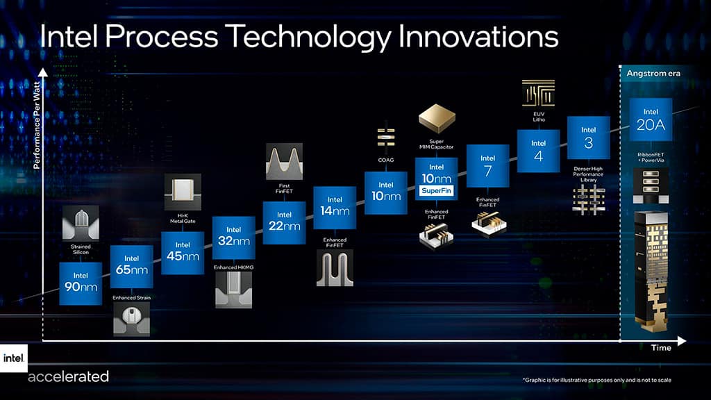 After the publication of the financial report, Intel shares fell 10%.
Mortgages for IT professionals: what you need to know
IT industry support
Revenue growth in the third quarter of 2020 was demonstrated by only two areas of Intel’s business — the segment of client products (+1%) and the Mobileye division (+2%).
AMD is still ahead of
Even Intel’s lack of its unnamed obstacle to 7nm prevents it from catching up with AMD, which releases all of its modern processors to these standards. It does not have its own factories, and the Taiwanese company TSMC is engaged in production, which successfully mastered 5 nm in 2020 and produces the Apple A14 processor using this topology.
AMD roadmap until 2020
In the first half of October 2020, as CNews reported, AMD held a demonstration of the new Ryzen 5000 line of processors armed with the latest Zen 3 architecture. They are also 7nm, but as part of a collaboration with TSMC, AMD has already set its sights on 5nm.
According to its roadmap, Zen 3 will be the last architecture to exploit 7nm. It will be replaced by Zen 4, already 5nm, and scheduled for release in 2021.
- In which data center will the Colocation equipment be placed? Find the answer on the IT marketplace Market.CNews
Elyas Kasmi
10nm Emerald Rapids, 7nm Granite Rapids, 5nm Diamond Rapids, up to 144 Lion Cove cores by 2025
Max Schapp | 2022/01/21
Intel has yet to announce a proper roadmap for their next generation Xeon processors, and while they have outlined their next generation products, we don’t know much, whereas AMD has offered early numbers regarding their 5nm EPYC processor line. So, The Next Platform, relying on their sources and a bit of speculation, have compiled their own roadmap, covering the Xeon family from Intel to Diamond Rapids.
Next Generation Intel Xeon Processor Rumors Emerald Rapids, Granite Rapids, and Diamond Rapids: Up to 144 Lion Cove Cores by 2025
As a cautionary note, the specifications and information published by TheNextPlatform are mostly estimates based on speculation and rumor, as well as hints from their sources. These are by no means Intel-verified specs, so take them with a pinch of salt. However, they give us an idea of where Intel might be heading with its next-generation lineups.
Intel Xeon processor generation roadmap (source: The Next Platform):
Intel Xeon processor generation IPC upgrade (source: The Next Platform):
4th Generation Intel Sapphire Rapids-SP Xeon Processor
Family
The Intel Sapphire Rapids-SP Xeon processors will be the first processors to feature a stacked chiplet. The SOC will include the latest Golden Cove core architecture, which will also be used in the Alder Lake lineup.
Team Blue plans to offer a maximum of 56 cores and 112 threads with a TDP of up to 350W. AMD, on the other hand, will offer up to 96 cores and 192 threads with TDPs up to 400W with their EPYC Genoa processors.
The AMD
will also have a big edge when it comes to cache sizes, I/O capabilities and more (higher PCIe lanes, higher DDR5 capacities, higher L3 cache).
The
Sapphire Rapids-SP will be available in two configurations: standard and HBM. The standard variant will have a chiplet design consisting of four XCC dies with a die size of about 400 mm2. This is the die size for a single XCC die, and there will be four in total on the top Sapphire Rapids-SP Xeon chip. Each die will be interconnected via EMIB with a 55 micron pitch and a 100 micron core pitch.
The standard Sapphire Rapids-SP Xeon chip will have 10 EMIB interconnects and the total package area will be an impressive 4446mm2. Moving on to the HBM variant, we get an increased number of interconnects, which are 14 and are needed to connect the HBM2E memory to the cores.
The four HBM2E memory packs will have 8-Hi stacks, so Intel is going to install at least 16GB of HBM2E memory per stack, for a total of 64GB in the Sapphire Rapids-SP pack. Speaking of packaging, the HBM variant will measure an insane 5700mm2 or 28% more than the standard variant. Compared to the recently leaked EPYC Genoa figures, the HBM2E package for Sapphire Rapids-SP will be 5% larger and the standard package will be 22% smaller.
- Intel Sapphire Rapids-SP Xeon (standard package) — 4446 mm2
- Intel Sapphire Rapids-SP Xeon (HBM2E kit) — 5700 mm2 that the top SKU will offer base frequencies up to 2.3GHz, 4TB DDR5 memory support, 80 PCIe Gen 5.0 lanes, and 350W peak power. Sapphire Rapids-SP Xeon line will offer up to 66% performance improvement over Ice Lake-SP chips and 25.9% performance/price improvement%.
The
Intel also claims that the EMIB channel provides twice the bandwidth density and 4 times the power efficiency of standard chassis designs. Interestingly, Intel is calling the newest Xeon line logically monolithic, which means they mean an interconnect that will offer the same functionality as a single die, but technically there are four chiplets that will be connected together.
The
AMD did make a difference with its Zen-based EPYC processors in the server segment, but it looks like Intel is planning to revive its future Xeon processor families. The first course correction will be Emerald Rapids, which is expected to launch in the first quarter of 2023.
5th Generation Intel Emerald Rapids-SP Xeon Processor
Family
The Intel Emerald Rapids-SP Xeon processor family is expected to be based on the Intel 7 node. You can think of this as a 2nd generation «Intel 7» node, which will result in slightly higher efficiency.
Emerald Rapids is expected to use the Raptor Cove core architecture, which is an optimized variant of the Golden Cove core providing 5-10% IPC improvement over Golden Cove cores. It will also feature up to 64 cores and 128 threads, which is a slight core increase from the 56 cores and 112 threads featured on the Sapphire Rapids chips.
The
is expected to have base frequencies up to 2.6GHz, 120MB L3 cache, memory support up to DDR5-5600 (up to 4TB), and a slight increase in TDP to 375W.
 Performance is expected to increase by 39.5% over Sapphire Rapids and the performance/price ratio is expected to increase by 28.3% over Sapphire Rapids. But most of the performance gains will come from clock speed and process optimizations on the Intel Enhanced Node 7 (10ESF+).
 By the time Intel releases the Emerald Rapids-SP Xeon processors, AMD has reportedly released their Zen 4C-based EPYC Bergamo chips, so the Xeon line might be too small and too late as only Intel’s extended instruction sets support them. The good news for Emerald Rapids is that it will remain compatible with the Eagle Stream (LGA 4677) platform and offer increased PCIe lanes up to 80 (Gen 5) and faster DDR5-5600 memory speeds.
6th Gen Xeon
Intel Granite Rapids-SP Processor Family
Moving on to Granite Rapids-SP, this is where Intel really starts making big changes to its lineup. For now, Intel has confirmed that its Granite Rapids-SP Xeon processors will be based on the «Intel 4» (previously 7nm EUV) technology node, but according to leaked information, Granite Rapids placement is moving around in roadmaps, so we’re not exactly sure.
 when the chips actually hit the market. It is possible that this will happen sometime between 2023 and 2024, as Emerald Rapids will serve as an interim solution rather than a full replacement for the Xeon family.
 Granite Rapids-SP Xeon chips are said to use the Redwood Cove core architecture and have an increased core count, although the exact number has not been revealed. Intel teased a general overview of their Granite Rapids-SP CPU during their «fast track» keynote, which appeared to show multiple dies packaged in a single SOC via EMIB.
We can see HBM packets along with high speed Rambo Cache packets. The compute tile appears to be 60 cores per die, for a total of 120 cores, but you should expect some of those cores to be disabled to improve performance on the new Intel 4 Technology Node.0007
AMD will be increasing the core count of their own Zen 4C EPYC line with Bergamo, bringing the core count to 128 cores and 256 threads, so even though Intel has doubled the core count, they still can’t match AMD’s breakthrough multithreading and multithreading .
But in terms of IPC, this is where Intel can start to approach the AMD Zen architecture in the server segment and get back in the game.
The
is said to have up to 128 PCIe Gen 6.0 lanes and a TDP of up to 400W. CPUs will also be able to use up to 12-channel DDR5 memory at speeds up to DDR5-6400. The performance gain over Emerald Rapids will almost double due to doubling the number of cores and improved core architecture, while overall performance/price is expected to increase by 50%.
One interesting feature mentioned by TheNextPlatform is that starting with Granite Rapids, Intel Xeon processors will use the latest AVX-1024/FMA3 vector engines to improve performance in a variety of workloads. Although this would mean that the power figures using these instructions would go up significantly. Granite Rapids and future Xeon processors will be compatible with the new Mountain Stream platform.
7th Generation Intel Diamond Rapids-SP Xeon Processor Family
Come to Diamond Rapids-SP and then maybe Intel will finally have a big win over AMD since its first EPYC launch in 2017.
The Diamond Rapids Xeon processors are touted as «large» in the leak and are expected to launch by 2025 with a radical new architecture that will be positioned against Zen 5.
The EPYC Turin line based on Zen 5 will not be slow moving as AMD is aware that Intel plans to return to the data center and server segment. There is no word yet on what architecture or number of cores the new chips will offer, but they will provide compatibility with the same Birch Stream and Mountain Stream platforms that the Granite Rapids-SP chips will also support.
7th Generation Diamond Rapids Xeon processors are expected to feature Lion Cove Advanced Cores on Intel Technology Node 3 (5nm) and offer up to 144 cores and 288 threads. Clock speeds will gradually increase from 2.5 to 2.7 GHz (tentatively).
In terms of IPC improvement, Diamond Rapids chips are expected to provide up to 39% performance improvement over Granite Rapids. It is expected that the overall performance will improve by 80% and the performance/price ratio will improve by 40%.
For the platform itself, the chips are expected to offer up to 128 PCIe Gen 6.0 lanes, support for DDR6-7200 memory, and up to 288MB of L3 cache.
The Diamond Rapids-SP lineup is not expected by 2025, so it’s still a long way off. Also mentioned is the Sierra Forest, which is not a successor but a variant of the Diamond Rapid-SP Xeon line that will target specific customers such as AMD Bergamo or the HBM variants of Sapphire Rapids-SP. It will definitely appear after Diamond Rapids-SP by 2026.
Intel Xeon SP families:
Family Branding Skylake-SP Cascade Lake-SP/AP Cooper Lake-SP Ice Lake-SP Sapphire Rapids Emerald Rapids Granite Rapids Diamond Rapids Process Node 14nm+ 14nm++ 14nm++ 10nm+ Intel 7 Intel 7 Intel 4 Intel 3? Platform Name Intel Purley Intel Purley Intel Cedar Island Intel Whitley Intel Eagle Stream Intel Eagle Stream Intel Mountain Stream
Intel Birch StreamIntel Mountain Stream
Intel Birch StreamMCP (Multi-Chip Package) SKUs No Yes No No Yes TBD TBD (Possibly Yes) TBD (Possibly Yes) Socket LGA 3647 LGA 3647 LGA 4189 LGA 4189 LGA 4677 LGA 4677 LGA 4677 TBD Max Core Count Up To 28 Up To 28 Up To 28 Up To 40 Up To 56 Up To 64? Up To 120? TBD Max Thread Count Up To 56 Up To 56 Up To 560791 Up To 112 Up To 128? Up To 240? TBD MAX L3 Cache 38. 5 MB L3
38.5 MB L3 38.5 MB L3 60 120 MB L3 MB L3 TBD TBD Memory Support DDR4-2666 6-Channel DDR4-2933 6-Channel Up To 6-Channel DDR4-3200 Up To 8-Channel DDR4-3200 Up To 8-Channel DDR5-4800 Up To 8-Channel DDR5-5600? TBD TBD PCIe Gen Support PCIe 3.0 (48 Lanes) PCIe 3.0 (48 Lanes) PCIe 3.0 (48 Lanes) PCIe 4.0 (64 Lanes) PCIe 5.0 ( 80 lanes) PCIe 5.0 PCIe 6.0? PCIe 6.0? TDP Range 140W-205W 165W-205W0791 Up To 350W TBD TBD 3D Xpoint Optane DIMM N/A Apache Pass Barlow Pass Barlow Pass Crow Pass Crow Pass? Donahue Pass? Donahue Pass? Competition AMD EPYC Naples 14nm AMD EPYC Rome 7nm AMD EPYC Rome 7nm AMD EPYC Milan 7nm+ 0791
AMD Next-Gen EPYC (Post Genoa) AMD Next-Gen EPYC (Post Genoa) AMD Next-Gen EPYC (Post Genoa) Launch 2017 2018 2020 2021 2022 2023? 2024? 2025? Comparison of generations of Intel Xeon and AMD EPYC processors:
CPU Name Process Node / Architecture Cores / Threads Cache DDR Memory / Speed / Capacities PCIe Gen / Lanes TDPs Platform Launch Intel Diamond Rapids Intel 3 / Lion Cove? 144 / 288? 288 MB L3? DDR6-7200 / 4 TB? PCIe Gen 6. 0 / 128?
Up To 425W Mountain Stream 2025? AMD EPYC Turin 3nm / Zen 5 256 / 512? 1024 MB L3? DDR5-6000 / 8 TB? PCIe Gen 6.0 / TBD Up To 600W SP5 2024-2025? Intel Granite Rapids Intel 4 / Redwood Cove 120 / 240 240 MB L3? DDR5-6400 / 4 TB? PCIe Gen 6.0 / 128? Up To 400W Mountain Stream 2024? AMD EPYC Bergamo 5nm / Zen 4C 128 / 256 512 MB L3? DDR5-5600 / 6 TB? PCIe Gen 5.0 / TBD? Up To 400W SP5 2023 Intel Emerald Rapids Intel 7 / Raptor Cove 64 / 128? 120 MB L3? DDR5-5200 / 4TB? AMD EPYC Genoa0790 96 / 192 384 MB L3? DDR5-5200 / 4TB? PCIe Gen 5. 0 / 128
Up To 400W SP5 2022 Intel sapphire Rapids Intel 7 / Golden Cove 56 / 112 105 MB L3 DDR5-4800 / 4 TB PCIe Gen 5.0 / 80 Up To 350W Eagle Stream 2022 Intel’s new roadmap reveals processor releases through 2019
New Intel roadmap highlights processor releases through 2019
to school page…
Information from websites
iXBT,3dnews
New Intel roadmap highlights processor releases through 2019
September 15, 2016
Intel recently introduced
new generation of processors — Kaby Lake. True, so far
energy efficient mobile options. Recall, Kaby Lake is the representative of the new step
optimization, which was previously absent in the Intel scheme.Desktop Kaby Lake will be released early next year. As for future plans
processor giant, they were revealed by another roadmap.2016-17 CCG Mobile Product Roadmap
So, apart from the generation of Kaby Lake, the next one in Intel’s plans is Gemini Lake. These
processors will replace the still brand new Apollo Lake, that is, they will be focused on tablets
and various ultrabook options. Such CPUs (or SoCs, to be more precise) will be characterized by TDP 4-6
W, like the current generation. Gemini Lake should hit the market early in the fourth
quarter of next year.Literally immediately after them will be the Cannon Lake CPUs, which will be produced on a 10-nanometer
technical process. As already accepted, Cannon’s energy-efficient mobile solutions will be presented initially
Lake-Y and Cannon Lake-U with TDPs of 5.2 and 15W, respectively. That is, mobile Kaby Lake will exist
on the market for only a year, except for models with GT3e graphics, which will be replaced only in 2018 and
it will no longer be Cannon Lake.And these will be 10-nanometer Coffee Lake CPUs.
In the second quarter of 2018 they will be launched in
mobile segment, but only in the Coffee Lake-U variant with GT3e graphics and TDP 15/28 W. More
energy-efficient models will remain representatives of Cannon Lake.At the same time, Coffee Lake will appear in the desktop segment. And it will be immediately six-core
CPU with a TDP of 45 W and the roadmap has no mention of other options. Apparently, only
the most productive models. That is, we can definitely count on the appearance of relatively
available six-core Core i7 variants in a year and a half.Source:
AnandTechIntel puts 10nm fabric into operation, pilot production starts this quarter
August 2, 2016
3dnews Alexey Stepin
Intel Corporation announces that it has finally successfully launched its new semiconductor factory,
the technological process on which implies the use of 10-nanometer standards. Soon
the start of production of the first samples of chips is expected, made using a new, even more
thin, rather than mastered now, technical process.In addition, the company confirmed that it has already begun
deliveries of Kaby Lake processors to customers. The cost of the new factory is huge, you can estimate it
will be by learning Intel’s third-quarter financials, which will include its value.Since no serious problems have been reported so far, it can be assumed that the publication
Cannonlake’s 10nm family of processors will take place on schedule. The first batches of processors can be
received already this year, and the new factory should reach its design capacity by the end of the first
quarter of 2017. Despite all the delays, Intel manages to remain at the forefront of the semiconductor industry.
production: although its 14nm process was delayed by 6-9 months, the technology company
continues to outperform its main and most dangerous competitors, which have their own production facilities with
thin technical processes — Samsung and TSMC.According to Intel, all the innovations and improvements that saw the light of day with the introduction of
14nm process technology will be retained in the new 10nm process.Will be raised
packing density, and the cost of products in terms of the transistor will decrease significantly.
The only serious problem that Intel has to deal with right now is the laws
the physical world. Already at element sizes in the region of 10 nanometers, quantum
effects, and with 7-nm and thinner technical processes, the task of combating them will rise to its full height. But
Intel says 10nm process won’t be a problem and deployment will take 50%
less time than it was with the 14nm process technology.
The company, of course, is already groping for new, even finer technical processes. After 7 nm it
seriously considers a range of materials and technologies. The list includes not only extreme
ultraviolet photolithography (EUV), but also various novelties that have not yet left
laboratories — for example, nanotubes, nanowires and graphene materials. More work to come
a lot, and Intel has not yet decided which horse to bet on in the process technology race, so
She is conducting a number of parallel studies.As for Kaby Lake, these are the latest processors
tick-tock generations. In fact, they are products of 14-nm polished to perfection.
technical process. Unfortunately, only
mobile versions of Kaby Lake-U.In the Zauba database, you can sometimes find
a lot of interesting information. For example, there appeared a description immediately 11
Skylake generation Intel Xeon V5 server processor models. To
unfortunately, the models are not indicated, and the available information refers to
engineering samples, so, for example, the frequency of serial CPUs can
be somewhat different.Whatever it was, let’s give all the available data.
No. of cores/threads Frequency, GHz L3 cache size, MB TDP, W 4/8 > 2. 0
8.25 105 10/20 > 1.0 13.75 73 12/24 > 1.0 16.5 105 14/28 1.8 19.25 135 16/32 1.5 22 135 16/32 1.8 22 135 16/32 2.4 22 165 20/40 1.8 27.