AMD launches Kaveri processors, aimed at starting a computing revolution
Interested in learning what’s next for the gaming industry? Join gaming executives to discuss emerging parts of the industry this October at GamesBeat Summit Next. Register today.
Advanced Micro Devices is launching its code-named Kaveri processors today, which represent one of the biggest technical advances that the company has made in some time. Kaveri chips are meant for games and other high-performance applications.
Above: Kaveri has 2.4 billion transistors.
Image Credit: AMD
The new chips show that AMD is moving in a very different direction from Intel, which at last week’s 2014 International CES put a lot of emphasis on “perceptual computing,” or using gestures and other new kinds of interfaces to control computers. Instead of interfaces, AMD is focusing on powerful graphics capabilities. AMD says Kaveri has 2.4 billion transistors (the basic building blocks of computer electronics), and 47 percent of them are aimed at better, high-end graphics.
Although the code name is Kaveri, the new chips will officially be called the A-Series Accelerated Processing Units (APUs). Like most AMD processors, they combine both graphics and central processing unit functions on the same chip. AMD’s chips will include up to four CPUs and eight graphics processing units (GPUs) on a single piece of silicon.
Nine out 10 PCs are now shipping with CPUs and GPUs on the same chip, according to Jon Peddie Research.
The Kaveri line is the first series of chips to use a new approach to computing dubbed the Heterogeneous System Architecture (HSA), which makes it easier to get around bottlenecks inside a PC and speed the whole system up.
Kaveri chips also include Graphics Core Next (GCN), an architecture designed for next-generation games.
AMD claims that its GPUs are much more powerful than Intel’s. For example, AMD said that its A10-7850K chip is 24 percent faster than the system performance of the higher-priced Intel Core i5-4670K chip. It says its graphics performance is 87 percent better than Intel’s, and its compute performance is 63 percent better than Intel’s.
AMD says the new chips will also use Mantle, an applications programming interface that makes it easier for developers to write high-performance games for AMD chips — it’s kind of like AMD’s own version of Microsoft’s DirectX technology. The chips will also have AMD TrueAudio technology, a 32-channel surround audio technology. The A-series chips will support screen resolutions up to 4K, or UltraHD, which puts four times as many pixels on a screen as 1080p high-definition TV.
Above: AMD Kaveri benchmarks
Image Credit: AMD
“AMD maintains our technology leadership with the 2014 AMD A-Series APUs, a revolutionary next generation APU that marks a new era of computing,” said Bernd Lienhard, corporate vice president and general manager of the client business unit at AMD. “With world-class graphics and compute technology on a single chip, the AMD A-Series APU is an effective and efficient solution for our customers and enable industry-leading computing experiences.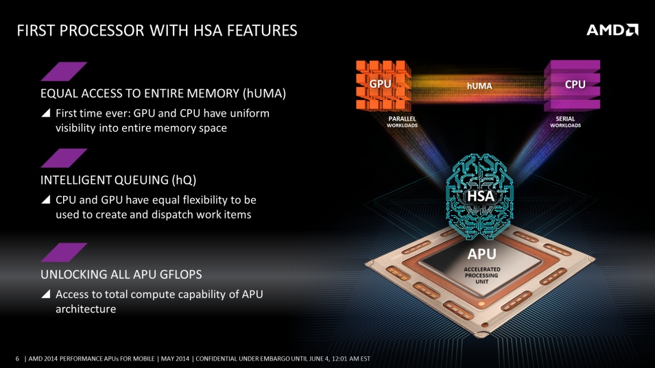 ”
”
HSA is pretty arcane technical material for consumers, but if it takes off, AMD says it will lead to faster and more power-efficient personal computers, tablets, smartphones and cloud servers. It goes hand-in-hand with hUMA, a new way for processors to access the memory inside an Accelerated Processing Unit, or a single chip that combines both a microprocessor and graphics.
The problem is that it isn’t easy for programmers to harness the power of the GPU, or graphics processing unit, inside an APU. The HSA has been designed to fix this problem, making graphics an equal partner with the CPU (central processing unit) and other processors, such as a digital signal processor, inside a computing system.
All of these functions used to be part of separate chips. But now they can be packaged inside the same system-on-chip, or SoC, on the same piece of silicon. The three different kinds of processors access data in different ways, but AMD wants to change and simplify that.
Above: AMD APUs target a lot of applications.
Image Credit: AMD
GPUs can be used for non-graphics computing tasks, but it often takes too long to route requests for data through a CPU. Most developers don’t want to deal with the difficulty of optimizing their code for this kind of work. But a new technique, dubbed “heterogenous queuing,” allows applications to directly communicate with the GPU, treating it as an equal partner along side a CPU when it comes to accessing data quickly. That means an application won’t have to wait for the CPU when what it really needs to is to access the GPU.
With HSA and heterogenous queuing, the GPU doesn’t have to wait for the CPU to feed it data. It can spawn its own tasks on its own.
Nathan Brookwood, an analyst at Insight 64, calls this change the “same kind of conceptual breakthrough that the introduction of the virtual memory wrought in the 1970s,” when engineers figured out a better way to manage memory in a computer.
AMD also said that Mantle will make it easy for developers to access new features in graphics chips. It allows developers to write games “closer to the metal,” getting rid of some of the overhead associated with running a PC and letting them get more access to the hardware’s real firepower.
In a demo called Star Swarm, Oxide Games created a Mantle-based science fiction scene with a gigantic space battle involving thousands of spaceships.
Patrick Moorhead, analyst at Moor Insights & Strategy, said, “Kaveri is the most interesting chip AMD has launched in years, and I really like what I have seen so far with third-party benchmarks on next generation workloads. It really is the culmination of the seven years since AMD acquired ATI.”
He added, “Kaveri’s market success will be directly proportional to the speed at which [it] can enable more and more software to become HSA-aware, where it can much more easily tap into the gigaflops of the GPU’s performance. AMD now needs either a Google or Microsoft to commit to optimizing their operating system for HSA to seal the deal, as it will make software that much easier to write.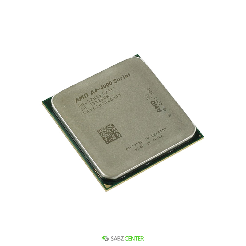 ”
”
The new A-Series chips will range in price from $119 to $173, while the power consumption will range from 45 watts to 95 watts. CPU frequency ranges from 3.1 gigahertz to 4.0 gigahertz. The A-Series APUs are available today.
Above: AMD HSA speeds graphics and CPU processing.
Image Credit: AMD
GamesBeat’s creed when covering the game industry is «where passion meets business.» What does this mean? We want to tell you how the news matters to you — not just as a decision-maker at a game studio, but also as a fan of games. Whether you read our articles, listen to our podcasts, or watch our videos, GamesBeat will help you learn about the industry and enjoy engaging with it. Discover our Briefings.
AMD Kaveri APU Architecture, Specifications And Prices Revealed
For AMD Kaveri APU Gaming and General Performance, Please visit this link!
At CES 2014, AMD showcased several slides regarding the next generation Kaveri APU detailing its architecture, specifications and prices. The Kaveri APU lineup will be available to consumers in 2014 featuring the latest GCN and Steamroller architecture which would be unified with HUMA to deliver faster compute performance to end users.
AMD Kaveri APU Architecture, Specifications And Prices Revealed
The biggest architectural change Kaveri APU features is the use of the latest 28nm Steamroller architecture that is a true multi-threaded architecture focusing on enhancing the IPC (Instruction-Per-Cycle) by upto 20%. In each module, two separate threads are provided with their own parallel instruction decoder, due to enhancements, the Kaveri APU die measures at 245mm2 with 2.41 Billion transistors crammed inside the die. The Kaveri APU is built upon the 28nm SHP. Steamroller is a completely new architecture hence there are improvements across the board which can be seen in the slides at the end of this article.
The most significant enhancement Kaveri would adopt is the HSA (Heterogeneous System Architecture) powered with the new HUMA enhancements which allow coherent memory access within the GPU and CPU. HUMA would make sure that both the CPU and GPU would have uniform access to an entire memory space which would be done through the memory controller. This would allow additional performance out of the APU incase the GPU gets bandwidth starved. This also suggests that faster memory speeds would result in better overall performance from the graphics card. Now with all the architectural talks done, let’s get on with the A10-7850K itself.
On the graphics side, we are getting the latest GCN architecture over the VLIW4 featured on previous AMD APUs. The die has upto 8 GCN compute units which feature AMD AudioTrue technology, AMD Eyefinity tech, UVD, VCE, DMA Engine and the addition of coherent shared unified memory. Being based on the same GPU as Hawaii, the Kaveri APU die has 8 ACE (Asynchronous Compute Engine) which can manage 8 Queues and have access to L2 Cache and GDS .
For the first time, AMD has called the GCN and Steamroller cores as the Compute Unit with 12 compute units (8 GCN and 4 Steamroller cores).
A compute core is an HSA enabled hardware block, that is programmable, capable of running atleast one process on its own context and virtual memory space, independently from other cores.
The Compute cores would be directly connected to a unified coherent memory.
The Kaveri APU can scale down to server platforms, from the high-end desktop PCs all the way to notebooks, servers and embedded applications. The Kaveri APU would come with TDP’s as high as 95W, down to 35W on mobility products and 15W in embedded applications.
For the lineup, AMD would launch only two APUs to kickoff 2014 which include the A10-7850K and A10-7700K while the A8-7600 would launch later in Q1 2014.
AMD A10-7850K
On with the specifications, the A10-7850K as expected would remain the flagship Kaveri APU of 2014 boasting 4 Steamroller cores, 4 MB L2 Cache and clock speeds of 3.7 GHz base and 4.0 GHz turbo. On the graphics side, the APU would feature 8 Compute Units resulting in 512 stream processors clocked at 654 MHz base and 720 MHz in boost. The APU is fully unlocked allowing users to overclock the chip past the limits and supports DDR3-2133 MHz and comes in a 95W TDP package. The A10-7850K would cost $173 US officially.
AMD A10-7700K
The A10-7700K is another unlocked chip featuring the Steamroller core architecture with a max boost clock of 3.8 GHz and base clock of 3.5 GHz. It features 4 MB of L2 cache while the GPU side ships with a GCN graphics die featuring 6 shader units equaling to a total of 384 Stream processors clocked at 720 MHz. The A10-7700K features a TDP of 95W so we may see one Kaveri APU part to feature 65W TDP. The A10-7700K would cost $152 US officially.
AMD A8-7600
The A8-7600 would be the last quad core variant in the Kaveri APU lineup featuring 3.1 GHz base and 3.8 GHz turbo frequencies with 4 MB L2 cache, 65W TDP and DDR3-2133 MHz support. The graphics side would include 384 Stream processors (6 Compute Units) and a core speed of 654 MHz base and 720 MHz boost. The APU would cost $119 US at launch. Specifications for the entire lineup can be seen here.
AMD Kaveri APU 2014 Lineup:
| Model | AMD A10-7850K | AMD A10-7700K | AMD A10-7800 | AMD A8-7600 | AMD A6-7400K | AMD A4-7300 |
| Cores | 4/4 | 4/4 | 4/4 | 4/4 | 2/2 | 2/2 |
| Unlocked Design | Yes | Yes | No | No | Yes | Yes |
| Base Clock | 3.7 GHz | 3.4 GHz | 3.5 GHz | 3.1 GHz | TBA | 3.4 GHz |
| Turbo Clock | 4.0 GHz | 3.8 GHz | 3.9 GHz | 3.8 GHz | TBA | 3.8 GHz |
| HSA Support | Yes | Yes | Yes | Yes | Yes | Yes |
| L2 Cache | 4 MB | 4 MB | 4 MB | 4 MB | 1 MB | 1 MB |
| Graphics Core | Radeon R7 | Radeon R7 | Radeon R7 | Radeon R7 | Radeon R5 | Radeon R5 |
| Compute Units | 8 | 6 | 8 | 6 | 4 | 3 |
| GPU Cores | 512 | 384 | 512 | 384 | 256 | 192 |
| GPU Clock | 720 MHz | 720 MHz | 720 MHz | 720 MHz | TBA | 514 MHz |
| TDP | 95W | 95W | 65W | 65W | 65W | 65W |
| Price | $173 US | $152 US | $172 US | $119 US | TBA | TBA |
AMD Kaveri APU Die Shot:
Following image is courtesy of Semiaccurate Forums!
AMD Kaveri APU Architecture and Slides:
Following images are courtesy of PurePC!
Review: AMD’s Kaveri APU examined — CPU
Abridged history of APUs
AMD has been steadily improving its premium Accelerated Processing Units (APUs) since the inception of the Llano processor in June 2011.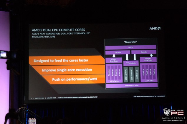
The first-generation APUs integrated AMD’s K10 CPU and Radeon HD 5000-series discrete graphics on to a monolithic die, thus enabling mainstream desktop and laptops to be powered by a single processor.
A major APU update, codenamed Trinity, arrived almost a year later, this time imbued with updated technology for both the CPU and GPU in the form of Piledriver cores and Radeon HD 6000 graphics, respectively, though the newer CPU architecture was often slower than the one it replaced. AMD, however, cemented its position as provider of best-in-class graphics through improvements to the GPU. Moving on another year to Richland, considered a minor refresh, AMD’s arguably kept ahead of Intel’s recent APU-like Core i3 and Core i5 processors in the all-important bang-for-buck-metric… but the gap is closing.
The newest APU technology now resides in ‘Kaveri’-based chips announced at CES last week. This time around and keeping up with the times, AMD fundamentally upgrades the graphics portion of the APU to the GCN architecture found in all the latest discrete Radeon GPUs and consoles whilst making incremental improvements to the CPU cores.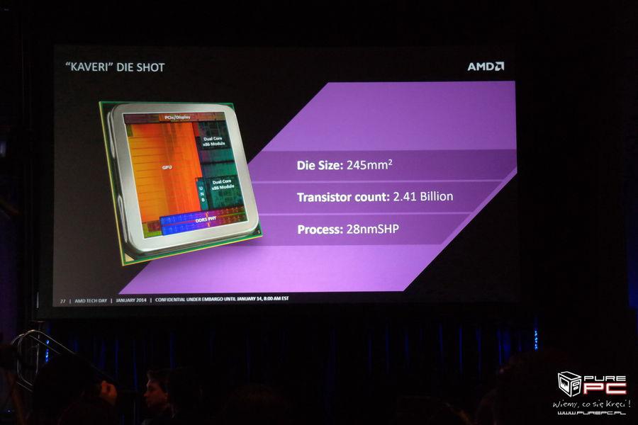
Brief APU comparison
|
APU Model |
Process |
CPU Cores |
CPU Tech |
Max CPU Clock |
GPU Cores |
GPU Tech |
Max GPU Clock |
AMD Turbo Core |
Form Factor |
TDP |
|---|---|---|---|---|---|---|---|---|---|---|
| Kaveri |
4 |
28nm |
Steamroller |
4.0GHz |
512 |
Radeon R7 |
720MHz |
Yes |
FM2+ |
95W |
| Richland |
4 |
32nm |
Piledriver |
4.4GHz |
384 |
HD 6000 |
844MHz |
Yes |
FM2 |
100W |
| Trinity |
4 |
32nm |
Piledriver |
4. |
384 |
HD 6000 |
800MHz |
Yes |
FM2 |
100W |
| Llano |
4 |
32nm |
Stars |
3.0GHz |
400 |
HD 5000 |
600MHz |
No |
FM1 |
100W |
 2GHz
2GHz
The high-level overview shows the key performance attributes of each AMD APU series. Let’s take the improvements turn by turn and thus evaluate whether Kaveri APUs offer a worthwhile upgrade over last-generation Richland.
28nm, does it matter?
AMD’s move down to a specific 28nm fabrication process has ramifications for the Kaveri APU beyond that of a smaller die. Joe Macri of AMD explained that previous APUs used silicon that was designed for frequency above denseness, a vestige of CPU design, thus optimising for MHz above parallelism by using speedy, low-metallised transistors. Now, as the GPU becomes more important — 47 per cent of the Kaveri die is devoted to it — and power is of greater concern, AMD, in conjunction with GlobalFoundries, is using an ‘APU-optimised’ process that offers a better compromise between all-out speed and ability to make the APU’s compute more parallel.
There are two key upshots from this. Firstly, the need to find a happy medium between performance, power and parallelism means this 28nm Super-High-Performance (SHP) process doesn’t have the ability to scale the cores as high as on previous APUs. We can see this by looking at the maximum speeds of both; the peak frequencies of the CPU and GPU parts is lower than Richland on a roughly-equivalent TDP. But secondly, use of 28nm SHP also allows AMD to shoehorn 512 graphics cores, which is comfortably higher than on any previous all-in-one processor. AMD’s adamant that this balanced design and wide dynamic range — the architecture has to fit into 15-95W TDPs — wouldn’t have been possible without the substantial tweaking undertaken here.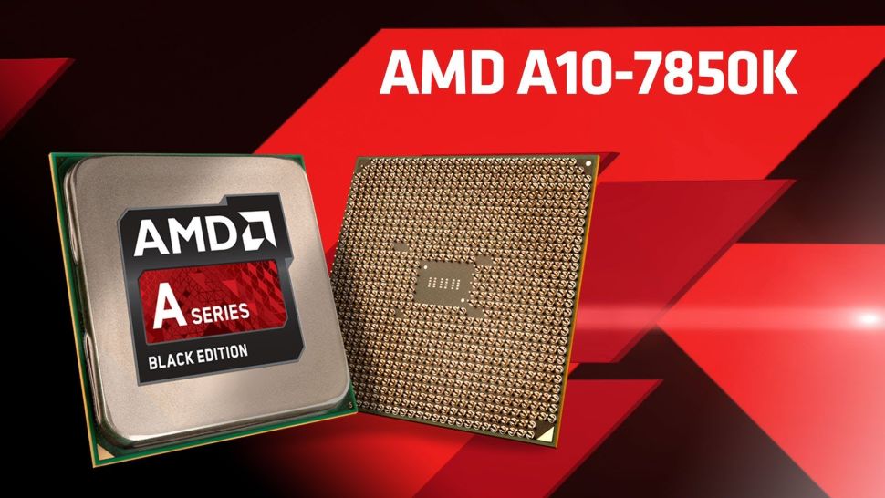
And it’s a big chip, too, weighing in at 2.41bn transistors, or over 1bn more than Trinity/Richland that it replaces. The AMD APUs share a die size of around 245mm², so not only does the 28nm process offer improvements in terms of gaining parallelism, it is very much needed in order to keep manufacturing costs sensible. As you can imagine, most of this extra transistor budget is for the graphics cores.
The steamin’ CPU cores
It is normal for AMD to harness the latest CPU technology present in discrete, standalone CPUs and use it in subsequent APUs. Trouble is, there is no new technology on this front, with AMD’s newest FX line of consumer CPUs still using the maligned Piledriver cores. Worse still, they won’t be upgraded until 2015 at the very earliest, intimating a tacit understanding that development has truly stalled on this front. This then leads AMD to take the rather unusual step of debuting new CPU tech on an APU — Kaveri is the first chip to use the Steamroller core.
Steamroller is an enhanced version of the Piledriver core, just as that was when compared to the original Bulldozer found in the first-generation FX chips. The basic architecture topology remains intact, but AMD has made some key changes with respect to efficiency, particularly at the fetch and decode stages of the pipeline, in an effort to boost throughput by reducing bottlenecks and stalling at the start of the compute process.
Getting more granular, the instruction cache has been boosted by 50 per cent, to 96KB, reducing misses by up to 30 per cent. The extra cost of silicon is worth it, says AMD, because misses here really hamper pipeline execution. Missing branches are also costly when processors become more parallel, so AMD doubles the branch target buffer. The scheduler, too, is improved, with Steamroller upping Piledriver’s 40 entries to 48. More is better because a wider scheduler enables the chip to be fed with instructions to a higher degree — efficiency by a different name.
There are also two distinct integer schedulers and ability to issue two stores at once, compared to one in the previous generation on each count. Looking at the backend, access to memory is improved by deepening the queues for load/stores, meaning that Steamroller can jump between main memory and the chip’s registers more quickly than either Richland or Trinity.
What does all of this mean in terms of real-world processing? AMD believes the improvements add up to an average 10 per cent uplift over Piledriver-based Richland in instructions-per-cycle (IPC) throughput, peaking at 20 per cent for best-case scenarios. The uptick in performance is about what we expected from a revised, enhanced core, but AMD will continue to play catch-up to Intel’s superior Haswell CPU architecture for some time to come: Steamroller isn’t a silver bullet, it’s a logical evolution of a below-par core.
Carrizo vs. Kaveri: Which low-end AMD CPU is a better buy?
- By Joel Hruska on July 18, 2016 at 10:28 am
This site may earn affiliate commissions from the links on this page. Terms of use.
When AMD launched its Carrizo CPU refresh last year, it made it clear that the chip would focus almost entirely on notebooks rather than desktops. The company just one low-cost part for the desktop space — the Athlon X4 845. This chip doesn’t use Carrizo’s updated integrated GPU, but packs in four cores in two CPU modules with a base clock at 3.5GHz and a 3.8GHz Turbo Mode. Based on AMD’s disclosures regarding Carrizo, the new chip should be faster and more efficient than the Kaveri cores it ostensibly replaced — but the truth turns out to be a bit more complicated.
Over at Anandtech, they’ve taken AMD’s latest core and matched it against previous parts based on Kaveri, Richland, and Trinity. The result is a 26-page magnum opus that compares the various chips in a huge range of scenarios and tests, from gaming to general-purpose compute in Windows. Linux benchmarks are included, as are results on a number of Intel products. There’s a great deal of information packed into the article and I highly recommend it.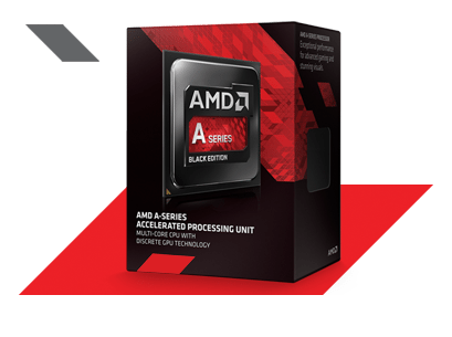
The big-picture takeaway on Carrizo versus Kaveri at the CPU level is this: There’s a solid group of tests where Carrizo shows real efficiency improvements over Kaveri. The graph below compares each APU to the previous generation and gives the improvement in percentage terms. A negative percentage means that the APU in question is slower than its predecessor, a positive percentage means the newer chip is faster.
Image by Anandtech
This is just one of the overall graphs in the review. Anandtech’s entire non-gaming Windows test suite measured the Athlon X4 845 as being 7.3% faster than Kaveri when all of the APUs were locked to 3GHz and tested at that clock speed. That’s not bad for a generational improvement, especially considering that the X4 845 is a 65W part compared with a 95W X4 860K.
Situational boosts
Unfortunately, Carrizo is dogged by two issues. First, its gains are situational. In some workloads, Carrizo is as much as 32% faster than Kaveri. In others, it’s 8-12% slower. Gaming takes a particular hit — Kaveri is approximately 6% faster than Carrizo when gaming, almost across the board.
Second, AMD was forced to pull clock speeds down when it shifted to Carrizo, just as it was when Kaveri debuted. The 65W Carrizo tops out at 3.8GHz with a 3.5GHz base, while the X4 860K is a 3.7GHz / 4GHz CPU. Anandtech reports that the overclocking headroom with their particular sample is small, at roughly 10%. Users would need to push the chip’s clock at least that high to count on matching Kaveri’s performance in the worst-case scenarios, though an OC’d X4 845 could also be substantially faster than the X4 860K.
Workloads that fit comfortably within Carrizo’s larger L1 cache (128K L1-D, compared to 64K for Carrizo) or benefit from its increased cache associativity (8-way, up from 4-way) show the largest improvements. Other tests show Kaveri winning past its newer cousin, presumably thanks to a combination of higher clocks and a larger L2 cache. This core was originally designed for laptops and it shows — the smaller L2 cache and eight lanes of PCIe 3. 0 may have been smart tradeoffs in the 15-25W space, but this is a 15W chip competing against desktop processors. Just pushing the TDP up to 65W doesn’t mean that Carrizo was actually designed to compete in these power envelopes (as we discussed last year, Carrizo is actually optimized to outstrip Kaveri at lower power envelopes, but may not compete well against it in the 65W+ space).
Those of you who have followed AMD’s designs over the past few years are likely aware that we saw a very similar pattern when Kaveri launched. Back in 2014, Kaveri proved it was an extremely potent replacement for Richland at the 45W TDP envelope but less persuasive at the 65W and 95W targets. Chips clocked above their sweet spot tend to require more voltage, which in turn generates more heat, which then requires more voltage… you get the picture.
On a more positive note, the competitive price ($70) and its quad-threaded design makes the X4 845 a very potent competitor against some of Intel’s dual-core CPUs like the 20th Anniversary Pentium it replaced last year. In the nearly four years since AMD’s first Piledriver-based APU launched, the company has managed to improve IPC (instructions per clock cycle, a measure of efficiency) by between 10% and 20% while simultaneously reducing power consumption. That’s a significant achievement, particularly for a company as cash-strapped as AMD, but it’s going to take Zen to really move the bar on the company’s overall performance-per-watt story.
When AMD announced Bristol Ridge earlier this year, we thought the chips and chipsets would be debuting already — but Computex has come and gone with no sign of the refresh. If Bristol Ridge doesn’t debut soon, it’s possible that AMD will hold the cycle for a CES announcement, presumably alongside Zen. Sunnyvale continues to insist that its next-generation CPU will sample late in Q4 for a Q1 2017 launch, but Zen’s first iteration is CPU-only. AMD will still need an APU to pair it with, which means 28nm Bristol Ridge APUs based on Carrizo will share space with 14nm Zen cores based on AMD’s new architecture. AMD hasn’t said when it’ll push Zen into APUs, but it’s safe to assume the company will make that transition as quickly as it can. Even if Zen-based APUs stick with DDR4 as their memory standard, the additional CPU performance and superior 14nm process make it a much more attractive part — assuming it hits its power and performance targets.
Bristol Ridge is unlikely to shake up the overall roadmap or Carrizo’s performance very much. While the chip will have some improvements and tweaks (and should support dual-channel memory in laptops) the typical gain for this kind of refresh is in the 3-5% range. Another 5% sure wouldn’t hurt the core’s CPU performance, but Zen’s 40% is what people are going to be watching for. If you’re looking to build an entry-level AMD gaming rig, Kaveri is probably the better option. If, on the other hand, you want a general-purpose system, Carrizo and the X4 845 may be the better core.
Now read: How L1 and L2 CPU caches work, and why they’re an essential part of modern chips
Tagged In
This site may earn affiliate commissions from the links on this page. Terms of use.
ExtremeTech Newsletter
Subscribe Today to get the latest ExtremeTech news delivered right to your inbox.
This newsletter may contain advertising, deals, or affiliate links. Subscribing to a newsletter indicates your consent to our
Terms of Use and
Privacy Policy. You may unsubscribe from the newsletter at any time.
More articles
Testing AMD Kaveri APU Dual Graphics Performance
February 14, 2014
Dino DeCesari
Reviews, Video Cards
Overclockers is supported by our readers. When you click a link to make a purchase, we may earn a commission. Learn More.
Table of Contents
There has been a lot of talk surrounding AMD’s Dual Graphics of late, especially since the release of the Kaveri APU lineup. Today, we’re going to explore the performance gains that can be had by leveraging the Kaveri A10-7850K’s built-in R7 graphics with a R7 250 discrete graphics card. AMD is constantly pushing affordable gaming to higher levels, and Dual Graphics with the latest Kaveri APUs is another example of this effort.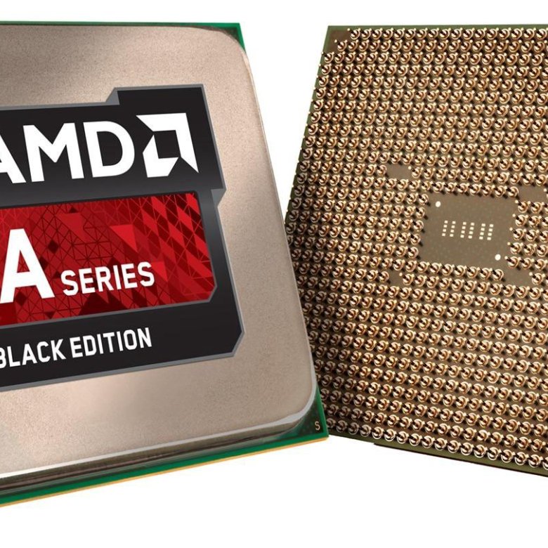 AMD sent along an MSI R7 250 OC Edition graphics card to test with, which is the series they recommend pairing with the A10-7850K. So let’s get going and see what Dual Graphics brings to the world of low cost gaming!
The MSI R7 250 OC Edition
We’ve already published a detailed review on the Kaveri A10-7850K, so we won’t spend time repeating what’s already been covered. If you haven’t yet read that review, click the provided link to be taken there. This article isn’t intended to be a full review on the MSI R7 250, but we will provide you with some pertinent information. We’ll start by giving you the specifications as provided by the MSI website.
| MSI R7 250 OC Edition Specifications | |
| Graphics Engine | AMD Radeon™ R7 250 |
| Interface | PCI Express x16 3.0 |
| Memory Type | DDR3 |
| Memory Size(MB) | 2048 |
| Memory Interface | 128 bits |
| Core Clock Speed(MHz) | 1050, Boost Clock: 1100 |
| Memory Clock Speed(MHz) | 1800 |
| DVI Output | 1 (Single-link DVI-D) |
| D-SUB Output | 1 |
| HDMI-Output | 1 (version 1. 4a) 4a) |
| HDCP Support | Y |
| HDMI Support | Y |
| Display Output (Max Resolution) | 1920×1200(SL-DVI-D) |
| RAMDACs | 400 |
| DirectX Version Support | 11.2 |
| OpenGL Version Support | 4.3 |
| CrossFire Support | Y(Software Support) |
| Card Dimension(mm) | 185x111x35mm |
| Weight | 352g |
…And here is a quick list of the key features.
|
||
Of note here is the increased clock speed from the reference design of an additional 50 MHz. The card also features 2 GB of GDDR3 memory, whereas most reference design cards are outfitted with 1 GB of memory. So, while the card is one of the lower end R7 offerings, it’s been beefed up a little for added performance.
Packaging/Closer Look
The red, white, and blue themed box does a good job of explaining the product inside. The front has some nice graphics and high level specifications, while the back gives a more detailed list of features and specifications. Inside the box, you’ll find a quick user’s guide, along with a driver/utility CD. Obviously, the utility is going to be MSI’s popular Afterburner overclocking software.
|
Packaging – Box Front |
Packaging – Box Back |
|
Packaging – Manual and Support CD |
Packaging – Protected Video Card |
Below is a set of pictures of the MSI R7 250 OC Edition. You’ll notice there is no auxiliary power required, and the card will run solely from the power provided by the PCI-E slot. The 2 GB of DDR3 memory is Hynix H5TQ2G63DFR. The cooling apparatus features MSI’s Propeller Blade technology and sits atop a solid aluminum heatsink.
|
MSI R7 250 OC Edition |
|
|
MSI R7 250 OC Edition |
MSI R7 250 OC Edition |
|
MSI R7 250 OC Edition |
MSI R7 250 OC Edition |
|
MSI R7 250 OC Edition |
MSI R7 250 OC Edition |
|
MSI R7 250 OC Edition |
MSI R7 250 OC Edition |
Recommended Pairing
There has been a lot of discussion about what exactly will work when pairing a Richland or Kaveri APU with a discrete video card. For Dual Graphics to work correctly, according to AMD, you’ll need to adhere to the table below. AMD states that R7 250 graphics cards with GDDR5 should also work fine.
The drivers AMD sent along for testing are version 14.1 Beta 1.6, which also include frame pacing enhancements. AMD claims these enhancements will allow for a smoother experience when Dual Graphics are enabled. AMD performed some in-house testing using Tomb Raider to illustrate the frame pacing enhancements. For those running Crossfire setups, it should come as good news that AMD is aggressively pursuing a fix for the “runt” frame issue that was reported several months back.
Enabling Dual Graphics
Once the discrete card is installed, all that’s needed to activate Dual Graphics is a quick trip inside Catalyst Control Center. From there, you can enable Dual Graphics from either the Gaming or Performance tab. If you wish to confirm that Dual Graphics is enabled during game play, there is an option to enable the Dual Graphics status Icon. To enable the icon, simply right click on the CCC icon in the system tray, and enable it from there. Dual Graphics will only work while gaming in full screen mode, and you will see the icon in the upper-right hand corner confirming Dual Graphics is in effect. Dual Graphics will not work if your game is running in windowed mode.
Dual Graphics Setup
Benchmarks
Here is the breakdown on the system we’ll be using for our benchmark session.
| Test System | |
| Motherboard | Gigabyte G1. Sniper A88X |
| APU | AMD Kaveri A10-7850K @ 4.0 GHz |
| GPU | MSI R7 250 OC Edition |
| Graphics Drivers | AMD Catalyst 14.1 Beta Version 1.6 |
| Memory | AMD Gamer Series DDR3 2400 2X4 GB Kit |
| CPU Cooling | Swiftech h320 LCS AIO CPU Water Cooler |
| PSU | Thermaltake Smart M 750 Watt |
| HDD | OCZ Vertex 2 240 GB SSD |
| OS | Windows 7 X64 SP1 |
Our intent today is to show the benefit of using Dual Graphics over the R7 iGPU, or just the discrete R7 250. With that in mind, we’ll compare results using just the APU’s R7 graphics, just the discrete R7 250 video card, and finally, both of them together with Dual Graphics enabled. Because a new set of beta drivers were introduced for improving Dual Graphics, I used those same drivers to test all three scenarios. The frame pacing option was enabled for the Dual Graphics testing.
As we usually do, we’ll take no prisoners and run all three of these scenarios through our updated GPU testing procedure. If you’re not yet familiar with our procedure, follow the link to learn more. Here is the down and dirty version of the test procedure we use.
Synthetic Tests
- 3DMark Vantage – DirectX 10 benchmark running at 1280X1024 – Performance preset.
- 3DMark 11 – DirectX 11 benchmark running at 1280X720 – Performance preset.
- 3DMark Fire Strike – DirectX 11 benchmark running 1920X1080 – Standard test (not extreme).
- Unigine Heaven (HWBot version) – DX11 Benchmark – Extreme setting.
Game Tests
- Batman: Arkham Origins – 1920X1080, 8x MSAA, PhysX off, V-Sync off, The rest set to on or DX11 enhanced.
- Battlefield 4 – 1920X1080, Ultra Preset, V-Sync off.
- Bioshock Infinite – 1920X1080, Ultra DX11 preset, DOF on.
- Crysis 3 – 1920X1080, Very high settings, 16x AF, 8x MSAA, V-Sync off.
- Grid 2 – 1920X1080, 8x MSAA, Intel specific options off, Everything else set to highest available option.
- Metro Last Light – 1920X1080, DX11 preset, SSAA on, Tessellation very high, PhysX off.
Starting with our synthetic testing, there are huge gains to be had with Dual Graphics enabled, as witnessed by the below charts. It’s interesting to note that the APU’s on die R7 graphics actually scored right on par with the discrete R7 250 OC Edition. So, if you were wondering what discrete card the Kaveri A10-7850K’s iGPU most directly compares to… here’s your answer.
|
HWBot Heaven Results |
|
3DMark Fire Strike Results |
|
3DMark 11 Results |
|
3DMark Vantage Results |
Our game benchmarks show the R7 250 OC Edition and the R7 iGPU swapping victories; and as expected, the Dual Graphics shows impressive gains throughout. While these raw FPS numbers might not look that impressive, you need to remember, all these games were set to their highest settings. If you lower a couple of settings, you’ll easily get a very playable experience at much higher FPS. If you’re wondering what settings get you these very playable FPS, I present you with a PDF file from AMD showing examples of what settings can be used for many of today’s popular game titles. (Click here for the file).
|
Batman: Arkham Origin Results |
|
Battlefield 4 Results |
|
Bioshock Infinite Results |
|
Crysis 3 Results |
|
Grid 2 Results |
|
Metro: Last Light Results |
Overclocking
Being that the thrust of this article is how to setup, use, and show what gains can be expected from Dual Graphics, I didn’t spend much time overclocking. However, I did spend a few minutes tinkering about. Just as a teaser, I overclocked the iGPU core to 1000 MHz in BIOS. GPU-Z only sees it as 960 MHz, so I’m not sure if the BIOS setting isn’t holding or if GPU-Z is reading incorrectly. I then used Catalyst Control Center to overclock the R7 250 OC Edition an additional 100 MHz core and 75 MHz on the memory. Only modest gains were noted with these small adjustments, but I’ll dive deeper into the overclocking prowess of this setup as time permits. Keep an eye on the forum post that coincides with this article for updates!
|
HWBot Heaven Overclocked |
3DMark 11 Overclocked |
|
3DMark Vantage Overclocked |
|
Conclusion
It’s hard not to like the gains we see when using Dual Graphics. It’s a powerful tool for obtaining better graphics performance and maintaining a low cost system build. The MSI R7 250 OC Edition is currently selling for $89. 99 at Newegg. To me, that’s a pretty small investment for the ability to run Dual Graphics. I certainly wouldn’t recommend buying one to use as a stand alone card, but it’s not really intended to be a serious gaming card on its own. However, coupled with a Kaveri iGPU and a few relaxed game settings, you will be on your way to a pleasurable and low cost gaming experience. If you currently own a Kaveri A10-7850K, I can easily recommend grabbing the MIS R7 250 OC Editions video card for the added Dual Graphics performance it will provide. Kudos to AMD for continuing to expand the available options for budget minded gamers!
–Dino DeCesari (Lvcoyote)
Dino DeCesari was a pillar of the Overclockers.com community for over 13 years when he passed away suddenly in 2015. His legacy lives on through his hundreds of computer hardware reviews posted here. Dino spent time in the army as a Telecommunication Center Specialist and received a commendation medal. He had a successful 20+ year career in the automotive parts and technology industry, where he eventually bought and sold his own business. Once retired, he volunteered as tech support for a non-profit and his local school district.
Related Articles
AMD A10-7850K Kaveri APU Review
AMD APUs continue to evolve with better graphics and compute performance with each new release. The Kaveri APUs are no different in this regard and attempt to redefine the landscape for what can be done on a single chip solution. Several new technologies have been introduced since the release of Trinity and Richland APUs, which we’ll explore today. AMD sent along the A10-7850K APU for us to have a look at, which is the flagship model for the Kaveri line. So, let’s dive into this latest APU offering from AMD and see what they have in store for us.
Specifications and Features
Here are the major specifications for the A10-7850K APU as pulled from the AMD press deck we were provided. There are a few things noticeable right from the start when looking at the below specifications. First, you’ll need a FM2+ motherboard (A88X chipset) in order to use the Kaveri APU. You can install the older Trinity and Richland APUs into a FM2+ motherboard, but Kaveri APUs won’t work on older FM2 (A85X chipset) motherboards. You’ll also notice that AMD has implemented support for 2400 MHz memory and their Mantle API for the iGPU.
A screen shot of CPU-Z and GPU-Z confirm much of what we see above.
Breaking away from the Piledriver core architecture found on the Trinity and Richland APUs, AMD has opted to use four Steamroller x86 cores on the Kaveri A10-7850K APU.
| Up to 4 “Steamroller” x86 computing cores |
|
The A10-7850K also incorporates eight GCN-based R7 series GPU cores, which support all of AMD’s latest technologies, including Eyefinity, 4K resolutions, TrueAudio, and dual graphics.
| Up to 8 GCN-based GPU cores |
|
The FM2+ platform offers several enhancements from previous AMD platforms. Most notable is official support for 2400 MHz memory, Crossfire, and PCI-E Gen 3.
| FM2+ Platform Highlights |
|
The HSA Heterogeneous Computing technology makes its debut with Kaveri APUs and promises better interoperability between the CPU and GPU cores. Both the hUMA (Heterogeneous Unified Memory Architecture) and hQ (Heterogeneous Queuing) work together to allow shared access to the system memory by both the CPU and GPU cores. This allows CPU and GPU cores to schedule tasks independently of each other. AMD claims 12 compute cores (4 CPU/8 GPU) linked together with the HSA technology, which in turn means GPU cores could theoretically handle tasks similar to the CPU cores. Software developers will need to optimize their applications to take advantage of HSA technology in order for us to reap the benefits, so hopefully, it will be widely adopted.
| HSA Hetereogeneous Computing |
|
AMD’s TrueAudio Technology makes its way to the R7 based iGPU found on the A10-7850K. Because TrueAudio has a dedicated DSP, it unloads that function from the CPU. This allows developers more freedom to enhance audio performance without impacting CPU performance.
| AMD TrueAudio Technology |
|
If you have been following the AMD APU products over the last couple of years, you may have noticed that the Kaveri A10-7850K actually has a reduction in both CPU and GPU clock speeds when compared to the Richland APU. The Richland A10-6800K CPU speed is 4.1 GHz stock/4.4 GHz boost, but the Kaveri A10-7850K sits at 3.7 GHz stock/4.0 GHz boost. However, AMD claims the Steamroller cores offer a 20% greater IPC (instructions per second) performance boost over previous APUs, which should actually equate to improved performance even at the reduced clock speed.
On the graphics side, we also see a reduction in clock speed from 844 MHz down to 720 MHz. However, by shifting to the GCN architecture and increasing the shader cores up to 512, we should actually see a performance boost over previous iGPU iterations. We’ll find out during our benchmark tests if the new technologies built into the CPU and iGPU indeed correlate to better performance, even at slightly slower clock speeds than the previous generation APUs. To that end, AMD’s own in-house testing does show impressive numbers when compared to their own A10-6800K and Intel’s i5-4670K.
Photo Op
Ok, so I admit it. A CPU or APU isn’t the most photogenic or interesting piece of hardware to look at. Nonetheless, we’ll do our due diligence and provide a few pictures for you. Worth noting is Kaveri’s pin count difference from Trinity and Richland, which is the reason you’ll need a FM2+ socket motherboard to accept the added pins.
|
AMD Kaveri A10-7850K APU |
|
|
AMD Kaveri A10-7850K APU |
AMD Kaveri A10-7850K APU |
|
AMD Kaveri A10-7850K APU |
|
Benchmarks
Test System
- AMD Kaveri A10-7850K APU
- ASRock FM2A88X Extreme6+ Motherboard (BIOS P2.
40)
- AMD Radeon Gamer Series DDR3-2400 MHz 2X4 GB Memory
- OCZ Vertex2 240 GB SSD
- Thermaltake Smart M 750 Watt PSU
- Swiftech h320 LCS AIO Water Cooler
CPU Side Testing
The first thing we’ll provide is a head-to-head comparison of the Trinity A10-5800K, Richland A10-6800K, and today’s A10-7850K review sample. The first set of tests will focus on CPU performance, which will give us a good idea of how AMD’s performance is progressing now that we are a few generations in. All the APUs were tested at their stock settings and with the memory set to their respective officially supported speeds.
Beginning with SuperPi and wPrime, we see very impressive gains when compared to the earlier APUs. When compared to the Richland A10-6800K, gains of anywhere from 15% to 21% were recorded. Those are pretty staggering numbers when you take into account the CPU is running 300 MHz slower than the Richland APU. The IPC enhancements AMD speaks of make themselves known here!
|
SuperPi 1M and wPrime 32M results |
|
SuperPi 32M and wPrime 1024M Results |
Cinebench R10 and R11. 5 show an ever so slight increase in performance over the Richland APU. While the Kaveri A10-7850K handily beat out the older Trinity A10-5800K, it was pretty much equal in performance to the A10-6800K and its 300 MHz faster clock speed. The scores are within the margin of error though, so it’s pretty much a wash between Kaveri and Richland here.
|
Cinebench R10 Results |
|
Cinebench R11.5 Results |
PoV Ray and x264 testing show the Kaveri A10-7850K again taking the win on all benchmarks. Here we see anywhere from a 3% to 6% gain in performance, depending on the test.
PoV Ray 3.73 and x264 Results
Here is a quick look at what AIDA64’s Cache & Memory Benchmark reports. No surprises here.
AIDA64 Cache & Memory Benchamrk
GPU Side Testing
As we migrate over to the iGPU testing, we’ll again compare performance against the Trinity A10-5800K and Richland A10-6800K. Because our GPU testing procedure has changed since the Trinity and Richland reviews were performed, I’ll have to resort to a few select benchmarks from the old suite of tests. I’ll also be able to toss in a couple Intel iGPU results for comparison here too. However, don’t think the Kaveri APU will escape our current testing procedure. We’ll run it through the full suite of games and compare it to a couple of lower-end discrete cards. This will give you a good idea of just how close AMD’s APUs are coming to discrete video card performance. Let’s begin the GPU testing from our older suite and use the Trinity, Richland, Intel 3770K, and 4770K for comparisons. Follow the links above to learn how each benchmark is configured.
The synthetic testing shows us a complete sweep for the A10-7850K. The three tests we used showed anywhere from a 26% gain all the way up to a staggering 50% gain in HWBot Heaven when compared to the Richland APU. Certainly nothing to argue about there.
|
3DMark 11 Results |
|
3DMark Vantage Results |
|
HWBot Heaven Results |
Continuing with our older game benchmarks, I chose four titles from that suite. Here again, we see the A10-7850K sweep the field as expected. All four of these games were set to their maximum settings. Given the results below, if you’re willing to lighten up on a few of the settings, a playable frame rate could easily be achieved.
|
Alien vs Predator Results |
|
Civilization V Results |
|
Dirt 3 Results |
|
Metro 2033 Results |
There is no denying the Kaveri A10-7850K is in a class of its own when it comes to integrated graphics. We were hoping to see AMD make noticeable gains in this area, and it appears they didn’t disappoint.
Moving over to our new GPU testing procedure, we’ll introduce an AMD reference R7 260 and HIS R7 250 into the mix. I went ahead and locked the A10-7850K at 4.0 GHz to match the frequency we test on the Haswell platform. It’s no secret that a discrete video card will perform better on a 4770K Haswell based system than on an AMD A88X based system, that much we know. So, given that we’re testing discrete video cards that were tested on the Haswell platform against Kaveri’s iGPU, we don’t expect the A10-7850’s iGPU to be able to keep up. However, it’ll be interesting to see what kind of gains have been made and how close to discrete-like performance AMD is getting with their APU progression.
Our synthetic tests show pretty much what we expected to see. While the A10-7850K’s iGPU couldn’t keep up with the discrete cards, the difference was less than we expected. Heck, I remember the days when you couldn’t even graph an iGPU on the same chart as a discrete card because of the huge number differences. Those days are gone, and the gap is definitely narrowing.
|
3DMark Vantage Results |
|
3DMark 11 Results |
|
3DMark Fire Strike Results |
|
HWBot Heaven Results |
Moving to our new set of games, we see the A10-7850K’s iGPU able to complete all the game tests under max settings. While the frame rates are far from playable under these conditions, relaxing a few settings will result in a playable experience. The take away from this is that AMD’s iGPU technology is definitely improving with each new release.
|
Batman: Arkham Origin Results |
|
Battlefield 4 Results |
|
Bioshock Infinite Results |
|
Crysis 3 Results |
|
Final Fantasy XIV: ARR Results |
|
Grid 2 Results |
|
Metro: Last Light Results |
Overclocking
Overclocking on the CPU side of things easily resulted in a 1 GHz overclock from the base clock of 3.7 GHz. This landed us at a stable 4.7 GHz with the memory still set to 2400 MHz. A quick 15 minute run of AIDA64’s System Stability Test, and we’re off and running! Pay no attention to the temperatures that AIDA64 shows, they are not accurate. AMD overdrive shows accurate temperatures, but in a manner we are not accustomed to seeing. AMD Overdrive now shows a thermal margin reading instead of the actual core temperatures. Supposedly, the thermal margin reading indicates how much headroom is left before the maximum operating temperature is reached. If the temperature monitoring is correct, it still shows a substantial amount of temperature headroom even with 1.45 V being sent to the CPU.
With the CPU at 4.7 GHz, let’s check a few benchmarks for performance increases. As you can see by the screenshots below, the A10-7850K scaled beautifully, and huge gains were had over our stock test results. Once again, there certainly isn’t anything to gripe about here.
|
SuperPi 1M at 4.7 GHz |
|
SuperPi 32M at 4.7 GHz |
|
wPrime 32M & 1024M at 4.7 GHz |
|
Cinebench R10 at 4.7 GHz |
|
Cinebench R11.5 at 4.7 GHz |
Ok, now that we have the CPU side overclocked about as far as it will go, let’s turn our attention to the iGPU side. Just to make sure the CPU side overclocking didn’t get in our way, I set it back to stock speeds for this testing. I’ll try to combine the two shortly. I was able to get the iGPU side up to 1000 MHz with only a sight bump in NB/GFX voltage. I ran 3DMark Fire Strike and HWBot Heaven at this speed; and just like we saw with the CPU overclocking, things scaled very well.
|
3DMark Fire Strike iGPU @ 1000 MHz |
|
HWBot Heaven iGPU @ 1000 MHz |
I think you’ll agree that the overclocking ability of this APU is pretty impressive and holds true for both the CPU and iGPU.
Pushing the Limits
Adding another 100 MHz to the CPU and another 20 MHz to the GPU put me right at the limit achievable without using dangerous voltages. I performed a quick run of SuperPi 1M and 3DMark Fire Strike at these speeds… pics below!
|
SuperPi 1M @ 4.8 GHz CPU / 1020 Mhz iGPU |
|
3DMark Fire Strike @ 4. |
Conclusion
AMD certainly improved the performance level of their APUs with the Kaveri release. You have to tip your hat to them for leading the way into the realm of heterogeneous computing. While it’s true software developers will have to adopt HSA for us to see the most benefit from it, you can’t deny the potential advantages it can provide should they decide to do so. Harnessing the compute power of both the GPU and CPU can only stand to benefit the end user, so hopefully, developers adopt the idea and provide applications that take advantage of it.
None of the tests we use take advantage of HSA, but we still witnessed good gains from previous APU releases. Even at a reduced CPU clock speed from that of its predecessors, the A10-7850K outperformed them due to improved IPC performance. However, these IPC gains have the potential to be minimized depending upon the task at hand as we saw in a couple of our tests. On the iGPU front, AMD continues to dominate, and it only got better this time around. Leveraging the R7 graphics, the GCN architecture, and TrueAudio, AMD continues to push iGPU capabilities. The Mantle API also makes its way to the iGPU this time around, so when and if game developers begin to utilize it on a large scale, it’ll be ready.
On the enthusiast front, overclocking was very fruitful. Both the CPU and iGPU overclocked extremely well and scaled nicely along the way. On a side note, I did use the AMD Overdrive software to do most of the overclocking, and it worked flawlessly. AMD Overdrive has all the tools you need to get the most from this APU right from the desktop… it certainly has matured over the years.
So, how much will this latest AMD APU cost you? You’ll be happy to know AMD has kept the sub $200 pricing intact. Newegg is currently offering the A10-7850K for $189.99 and that includes a Battlefield 4 game coupon too. Good deal? Most definitely!
I’ll reiterate what I said at the conclusion of the Richland APU review last year with AMD’s catch phrase of “the sum is worth more than the individual parts. ” To that end, AMD delivers again with the Kaveri A10-7850K. If you’re looking to build an inexpensive system or are a gamer that doesn’t mind turning a few settings below their maximum, this could be the all-in-one APU you’ve been looking for.
Click the stamp for an explanation of what this means.
– Dino DeCesari (Lvcoyote)
AMD Kaveri Mobile — evolution continues. Report / Processors and memory
At the beginning of the year, AMD introduced the Kaveri desktop processors. Even then, there was practically no doubt that the manufacturer would sooner or later release a mobile version of such hybrid chips. As a result, we had to wait almost half a year for this event — the official announcement of new APUs for laptops took place within the framework of the Computex 2014 exhibition. The processors are based on the modern Steamroller microarchitecture, and the chips are produced according to the “thinnest” technical process available from AMD — 28 nm. AMD calls the Kaveri APU the most advanced APU — indeed, the new products boast support for a number of unique technologies.
The Sunnyvale company prefers to think of Kaveri processors as 12-core solutions. In fact, there are only four CPU cores in Kaveri mobile APUs, the remaining eight are the graphics subsystem. However, this step of the company should not be considered an ordinary marketing ploy — of course, it could not have done without marketing, but AMD has reason to make these generalizations. It’s all about supporting the HSA (Heterogeneous System Architecture) specification, which provides for the ability to parallelize data processing by CPU and GPU cores. Thanks to hUMA (heterogeneous Uniform Memory Access) technology, all processing cores of the processor can use common memory and a single address space. This eliminates the need for additional copying of data during their processing by CPU and GPU cores and, in theory, should increase performance — of course, with software support.
The graphic component in AMD Kaveri processors is represented by Radeon R7 solutions based on the GCN architecture (in older models, in younger models solutions of previous generations are used — Radeon R6 and R5). This means that the Microsoft DirectX 11.2 API is supported, as well as AMD’s own Mantle technology, thanks to which the performance in some games can be doubled. The GPU in the top AMD Kaveri processor operates at a frequency of 686 MHz, and the theoretical total performance is declared at 818 Gflops. You can get acquainted with all the features of the AMD Kaveri processor architecture in a detailed review by Ilya Gavrichenkov.
Other interesting features of AMD Kaveri mobile processors include support for AMD proprietary technologies: TrueAudio, Eyefinity, Face Login, Gesture Control, Turbo Core, Quick Stream, Wireless Display, Perfect Picture, Start Now and Enduro. Of course, only older solutions fully support these technologies. For example, AMD Face Login allows you to log in to various websites using face recognition, which is carried out using a laptop webcam, so you do not need to drive in passwords. AMD Wireless Display technology lets you share content wirelessly for a seamless HD video experience.
So, the new family of AMD Kaveri mobile processors includes nine different models. An interesting point is the appearance of the AMD FX brand in mobile chips: two models, FX-7600P and FX-7500, should defend the honor of the once popular trademark. It is worth talking about the older chip in more detail — it is on its example that we will try to evaluate the performance gain of new processors compared to their predecessors. So, the AMD FX-7600P contains 12 «computing» cores (4 CPUs + 8 GPUs), operates at a frequency of 2.7 GHz, which can rise to 3.6 GHz in turbo mode, is equipped with 4 MB of L2 cache and can work with DDR3-2133 memory modules. Its TDP is capped at 35W.
We decided to compare the processor with one of its predecessors — the AMD A10-5750M APU and with a low-wattage Intel processor from the new 4th generation Intel Core i7-4200U series. We also tested the graphics part of the new APU and compared it not only with the previous solution — AMD Radeon HD 8650G, but also with the NVIDIA GeForce 840M discrete mobile video adapter built on the latest NVIDIA Maxwell architecture. Unfortunately, the time allotted to get acquainted with the new processor was limited to a few hours, so we physically did not have time to conduct a full cycle of tests. Also, the results of one of the PCMark 8 subtests — Creative — were taken from AMD for the reason already indicated.
| Comparable notebook specifications | |||||||
|---|---|---|---|---|---|---|---|
| Notebook | Display | Processor | Memory | Graphics | Accumulator | Battery | OS |
| AMD Kaveri Mobile Sample | 15.6″ 1920×1080 |
AMD FX-7600P; 2.7 (3.6) GHz, 2x 2MB L2; Quad Core, TDP 35W |
2 x 4 GB DDR3L-1866 | AMD Radeon R7 Series (Integrated in CPU) | SSD 256 GB (SAMSUNG MZHPU256HCGL) | Windows 8. |
|
| Lenovo G505S | 15.6″ TN 1366×768 |
AMD A10-5750M; 2.5 (3.5) GHz, 2x 2MB L2; Quad Core, TDP 35W |
2 x 4 GB DDR3L-1600 | AMD Radeon HD 8650G (Integrated in CPU) | HDD 1TB (Seagate ST1000LM024) | Removable, 41 Wh (2800 mAh, 14.88 V) |
|
| ASUS Zenbook UX32L | 13.3″ IPS 1920×1080 |
Intel Core i7-4200U 1.6 (2.6) GHz 3 MB L3; Dual core, TDP 15W |
1 x 6 GB DDR3L-1600 | NVIDIA GeForce 840M (2 GB GDDR3) | HDD 1 TB (HGST HTS541010A7E630) | Integrated, 50 Wh (4300 mAh, 11.3 V) |
|
Before proceeding to the tests, let’s remember how the acquaintance with the AMD A10-7850K desktop processor, the fastest of the new AMD Kaveri APUs, ended: vary depending on the angle from which you look at the novelty. The new processor is insanely interesting because it develops the concept of heterogeneous computing and introduces HSA technology, which allows software developers to easily move on to writing algorithms that run on the computing clusters of the graphics core. It seems that a little more — and AMD will ensure that new applications will work on its processors no worse than on Intel’s CPUs. To do this, Kaveri has all the necessary resources and, most importantly, a huge theoretical computing power, which lies in the graphics core. However, not all so simple. So far, there are not many even simple OpenCL-optimized applications, and the efficiency of existing implementations of heterogeneous computing leaves much to be desired. Another thing is games. Most modern games can be played on the A10-7850K in Full HD resolution, and many of them, such as popular network projects, work quite well even with medium or high image quality.
⇡#Testing the processor
Recall once again that the results of one of the subtests, namely PCMark 8 Creative, were provided by AMD for the reason that its «run» takes about two hours, and only four o’clock. Unfortunately, this subtest was done using the OpenCL workbench, with the video adapter assisting the processor. Usually the 3DNews test lab does not use this option for accelerating calculations, but this time we simply had no choice due to the lack of time allotted to get acquainted with the new mobile APU.
In the single-threaded audio content transcoding benchmark, the AMD FX-7600P processor was slightly faster than its predecessor and slower than its competitor from Intel.
In the benchmark made on the basis of Adobe Photoshop CS6, we see similar results, although there is one small clarification to be made here. The laptop with the new APU used an SSD drive, which could speed up the caching process when there was not enough RAM.
In the PCMark 8 test suite, we see the superiority of the new AMD FX-7600P over the old AMD A10-5750M in all three tests. But the Intel Core i7-4200U processor with a TDP of 17 W was faster than its competitors in the Work and Home subtests. In the Creative subtest, this CPU is not represented due to the fact that it had to be carried out using OpenCL, and the ASUS Zenbook UX32L ultrabook is no longer in the test lab.
In synthetic gaming tests, the new APU performed quite well. In the 3DMark synthetic benchmark, it’s almost twice as fast as its predecessor in all three tests. ASUS Zenbook UX32L does not participate in this discipline again, because the AMD test laptop had a new version of 3DMark installed, the test results of which are incompatible with our 3DMark 1.1.
In Bioshock Infinite, the AMD FX-7600P GPU almost managed to catch up with the NVIDIA GeForce 840M discrete video adapter, which is very good. At the minimum graphics settings and a resolution of 1366×768, the AMD Radeon R7 Series processor video core was able to overcome the barrier of 60 FPS, and at the maximum settings it came close to the NVIDIA discrete solution.
⇡#
Conclusions
As already noted, the testing was preliminary — we can draw full conclusions only after we receive the first commercial products based on AMD Kaveri Mobile and test it in our laboratory.
So, in the framework of testing processor cores alone, the superiority of the new APU with the Steamroller architecture compared to the old APU with the Piledriver architecture turned out to be quite noticeable, in contrast to the situation with desktop processors. Although the new processors are still unable to catch up with Intel solutions even with half the heat pack and the number of cores. However, it is worth noting that if all our benchmarks were compatible with HSA (Heterogeneous System Architecture) technology, which makes it possible to process the same data using the CPU and GPU, then the test results could be completely different. In its discussions about the power of new APUs, AMD focuses on such parallel computing, but how soon such a possibility will be implemented in software is up to software developers.
As for the graphics core, it turned out to be quite fast: in our benchmarks, it not only left its predecessor, AMD Radeon HD 8650G, far behind, but also managed to get quite close to discrete graphics cards of the NVIDIA GeForce 840M level, which is very OK. So with reasonable pricing, laptops based on the new AMD processors will be excellent low-cost solutions for gamers.
We would like to thank Ulmart for providing a Lenovo laptop for testing.
Introduction
In 2014, the first announcement for AMD was the introduction of another family of APUs, codenamed Kaveri. It was in this generation of APUs that it finally became clear why the company bought ATI a few years ago, known for its graphic solutions — to fully merge computing CPU and GPU cores. Kaveri combines many technologies designed specifically for universal computing: a unified graphics architecture, shared memory access, and other features of the HSA architecture. And the global goal of Kaveri is not just the release of the next solutions with integrated graphics for the most massive price segment, but a much more important task that AMD is moving towards, and which we will talk about later.
The CPU part of Kaveri is based on the third generation of AMD Bulldozer computing architecture — Steamroller cores. While the Piledriver core, which we know from the Trinity and Richland generations, brought improved power efficiency, the Steamroller should increase the number of instructions per clock executed by the microprocessor (AMD estimates IPC increased by 20%) compared to them, which is important to improve performance without the need for higher clock speeds. And the GPU part of the new APU family has finally moved from the VLIW architectures known from desktop graphics solutions of the past to the latest GCN architecture, which was first introduced in the Hawaii GPU. And most importantly, the CPU and GPU parts of the Kaveri chip were able to interact with each other with previously unseen capabilities.
The main innovation in terms of manufacturing process is that with the announcement of Kaveri there was a transition from the 32nm High-K Metal Gate SOI process technology to 28nm SHP («Super High Performance»), but in the same Global Foundries factories . There is a difference between the various options, if the 32 nm SOI Global Foundries process is optimized more for high-frequency CPUs, then the TSMC 28 nm process is better suited for GPUs, allowing for greater density. The main goal of the 28 nm SHP process technology is to achieve a sufficiently high transistor density, but with some loss in the maximum operating frequency, relative to 32 nm SOI. Therefore, it is not surprising that higher frequencies were not achieved in Kaveri compared to Trinity and Richland. But in general, this process technology is great for APUs, as it provides an optimal balance for the CPU and GPU parts of the chip.
The Kaveri die size is similar to what we saw in Richland (245 mm² vs. 246 mm²), while the novelty has significantly more complexity (2.4 billion transistors vs. 1.3 billion), which means a huge increase in density of transistors and a decent increase in process efficiency. Purely theoretically, the transition from 32 nm to 28 nm should have given an increase in density by a little more than a quarter, but by no means by 85%, as happened in the case of switching from Richland to Kaveri.
New APUs, perhaps, for the first time began to be mentioned by AMD as quite suitable for gaming applications. After all, it was difficult to imagine Llano and Trinity as gaming solutions, they were distinguished by rather weak CPU and GPU performance, which was clearly not enough for games. Although heterogeneous computing on Kaveri has become an even more serious claim, the new APUs differ in that they are quite capable of giving acceptable gaming performance in modern games. Of course, you can always say that in almost any game on any hardware, you can achieve 30 frames per second by lowering the settings. But AMD has set itself the goal of achieving acceptable performance without reducing resolution — choosing Full HD as a benchmark. It is clear that games like Battlefield 4 and Crysis 3 will also require lowering the settings from the maximum, but there are many games that will run fairly quickly on the new APUs and at high settings.
Changes in Kaveri in terms of additional features have also been quite significant. Not to mention the improvements in the Unified Video Decoder and Video Coding Engine video data processing units, we can separately highlight the integrated TrueAudio audio part, designed to reduce CPU load by complex audio calculations. According to AMD, TrueAudio technology will allow game developers to increase the number of sound effects and improve their quality, all while reducing the load on the CPU.
Still, the most important feature of Kaveri is HSA’s heterogeneous system architecture, which combines the power of CPU and GPU computing units, expanding the capabilities of the programming model for software developers. If in all previous solutions the CPU and GPU cores were considered exclusively separate execution units and required data to be copied from the memory of one to the memory of the other when working together, then in Kaveri the CPU and GPU parts can simultaneously work with the same data in a unified memory. Of course, it will be some time before these features are used in real software, but the possibility itself already means a lot to the industry.
AMD is going to solve all the problems of introducing heterogeneous computing and an updated programming model with the help of HSA and related utilities for programmers. AMD is trying to provide developers with the means to ensure that the full power of heterogeneous architectures costs them writing as little complex custom code as possible while parallelizing such tasks. The company has already provided many utilities and libraries for developers using OpenCL (by the way, Kaveri has everything you need to support OpenCL 2.0 and will be the first processor to support this version of the API), Java, C ++ and other programming languages.
In terms of market positioning, the Kaveri family of APUs are designed for several market segments at once, as the chip is highly scalable, providing high performance with limited power consumption of different levels. High power efficiency has been a top priority for Kaveri and the new APUs are great for laptops and other applications. So, Kaveri chips are already known, which are intended for market segments that limit the consumption level to 15 W, 45 W, 65 W and 95 W.
Collaboration of computing cores
In the case of many modern chips and systems-on-chips with numerous execution units, each manufacturer counts computing cores in its own way. Previously, in the characteristics of SoCs, the approach indicating the number of CPU cores was considered generally accepted — this is followed by companies such as Intel and Qualcomm, for example. Other companies have recently begun to classify others as «cores». For example, NVIDIA recently named its latest system-on-a-chip Tegra K1 as early as 192-core by counting all streaming CUDA GPU cores. So the question is certainly not an easy one.
Kaveri differs markedly from the first generations of APUs in terms of how CPU and GPU cores work together. If in the first generation Llano needed special interfaces to move data between computing cores and memory, then Trinity and Richland not only increased bandwidth, but unified memory access from the CPU and GPU, improved synchronization and made other improvements. Kaveri added to this the possibility of virtual memory with coherent access from two cores, as well as atomic operations to synchronize the load between different cores.
In the case of a GPU, it is generally very difficult to understand what is considered a separate “core”, which is why we see a big difference in these numbers from different manufacturers. It seems that the time has come to determine which part of the highly integrated chips can generally be called a separate core. It is clear that only the CPU and GPU cores need to be taken into account, and not auxiliary DSPs, ISPs, and others. In the case of AMD Kaveri, the APU architecture is completely unified and CPUs with GPUs can work on the same data at the same time, and almost half of the chip is given to the graphics cores in Kaveri, so the figure for the number of computing cores in this case should include both CPU and GPU -kernels, according to experts from AMD.
Therefore, AMD decided to introduce a new term: “compute core” (“compute core”), which can hide both the usual universal x86 or ARM architecture CPU core and the GCN architecture computing unit. That is, each executable data stream on the CPU will mean a separate «compute core» and each computing unit of the GCN architecture of the GPU will also be called a «compute core». The main thing is that each «computing unit» supports HSA, can run a dedicated process with its own context and virtual memory, completely independent of all other cores.
The total number of computing cores in the new APUs combines both the first and second types of computing units: CPU and GPU. In other words, the top Kaveri solution, which was released on the market under the name A10-7850K, according to such a counting system, has a total of 12 «computing cores»: four from the CPU (two Steamroller modules execute four threads simultaneously) and eight from the GPU (Kaveri graphics core contains eight blocks of the GCN architecture).
It seems that AMD has the right to count the cores in this way, because each «computing core» of the CPU or GPU can execute a separate code thread. The GCN architecture is versatile and flexible enough to run multiple independent programs per GCN block count, and previous generations of AMD graphics in APUs were limited to a single task per GPU.
On the other hand, the total number of blocks so different in essence says little, except for marketing, because 12 «computing cores» in Kaveri are not the same! Both from the point of view of a programmer who needs to write one code for CPU cores and completely different for GPU cores, and for a user who cannot run an Internet browser on GPU cores while CPU cores are busy with other tasks.
Therefore, the best way out seems to be to indicate two numbers among the characteristics of the new APUs: the total and separate number of CPU and GPU cores. For example, for the top solution A10-7850K, it is better to mention not only “12 computing cores”, but “4 CPU and 8 GPU cores”. This approach allows you to both provide technically correct data and not overly upset the AMD marketing department, who want to see big numbers. If only now such users do not appear who consider that they have a “12-core processor”, which is three times faster than the “4-core” top one from a competitor.
At the time of the announcement of the line, AMD offered the following configurations for its new APUs:
A10-7850K : 12 compute cores (4 CPUs and 8 GPUs)
A10-7700K : 10 compute cores (4 CPUs and 6 GPUs) )
A8-7600 : 10 cores (4 CPUs and 6 GPUs)
HSA Heterogeneous Architecture
Heterogeneous computing and capable hardware are becoming more and more widespread in various fields. So, almost all smartphones and tablets released over the past couple of years are based on chips that can be called heterogeneous processors. And in other segments things are going in the same direction. According to AMD, last year about 9Nine percent of Intel’s desktop processors and more than two-thirds of AMD’s processors contained integrated graphics. The same goes for modern gaming consoles. The latest generation of Sony and Microsoft set-top boxes are based on AMD’s heterogeneous processors.
Perhaps only server processors remain, where heterogeneous computing has not yet become so widespread. However, among the 500 most productive supercomputer systems in the world, several dozen already have a heterogeneous architecture, and there is a clear trend to expand this number. In addition, AMD has already introduced and plans to start shipping heterogeneous server processors in 2014.
So it’s safe to say that most modern processors are heterogeneous systems, and quite a large part of them are APUs. This is confirmed by statistics from Jon Peddie Research and IDC collected in the third quarter of 2013. Actually, the same trend is confirmed by statistics indicating the growth in the use of heterogeneous computing in software — there are more and more corresponding applications:
Open API for universal computing OpenCL is the standard for such tasks, it is supported by most software developers. But, unfortunately, far from all software that can benefit from heterogeneous computing (in particular, from transferring some tasks to GPU computing) uses these opportunities, since programming such systems is quite laborious.
To help spread heterogeneous computing, a non-profit HSA consortium was created at one time, in which a lot of companies already participate, including: AMD, Qualcomm, ARM, Oracle, etc. The list of AMD’s partners in promoting HSA is already enough big and growing all the time. The consortium is developing industry standards that make it easier to take advantage of heterogeneous computing devices like GPUs and others for greater performance. To do this, a special set of tools for programmers and developers is released, which allows you to more efficiently use the capabilities of the CPU, GPU, APU, FPGA and DSP.
AMD is making strides in the right direction as it expands developer software support by bringing HSA capability to a growing range of software environments, operating systems, and programming languages. With HSA capabilities, Kaveri’s new hybrid chips become one of the most suitable for heterogeneous computing. HSA features such as hUMA, Platform Atomics, and hQ are fully compliant with OpenCL 2.0 Fine Grained SVM, C11 Atomics, Dynamic Parallelism, and Pipes, making the Kaveri family of APUs the first chips to fully support OpenCL 2.0.
This slide shows just a few of the techniques that Kaveri can take advantage of to achieve higher performance with heterogeneous computing. And the next one shows an already possible advantage in one of these tasks — a binary search tree, which parallelizes well, which is a big advantage for heterogeneous APUs.
Among the specific applications in which the capabilities of HSA will be justified, we can name the following tasks, which are very demanding on computing power: gesture recognition, images, voice, biometric parameters, augmented reality systems (graphic and audio data that complement the real world), data streaming , new video and audio codecs, editing and transcoding data, searching and indexing multimedia data.
It is the capabilities of the heterogeneous HSA architecture that help Kaveri APU to reveal all the possibilities of its «computing cores», including graphics ones. The first introduced hUMA technology gives GPU and CPU equal access to a common address space in memory (up to 32 GB), hQ (heterogeneous queuing) technology determines the interaction between different cores and provides GPU and CPU cores with equal flexibility in operation.
Kaveri’s HSA-aware design should make it easier to develop heterogeneous software, increase the efficiency of using all 12 APU cores, and unleash the potential for parallel processing on CPU and GPU cores. But this requires not only hardware, but also appropriate software support: libraries, APIs, and utilities that facilitate the creation of complex programs.
More recently, AMD has been doing a lot to make heterogeneous systems easier to use by programmers using a variety of languages and libraries. So, for quite some time now, it has been possible to use the capabilities of GPU computing in Java programs. Java 7 introduced Aparapi, an API for executing well-parallelized algorithms on multi-core and multi-processor systems using OpenCL, in Java 8 Aparapi already uses HSA capabilities, and in Java 9 (Sumatra), which is expected to be released in 2015, it will already be full support for HSA specifications.
Naturally, the matter is not limited to Java alone. AMD has released a generic SDK that provides access to components to facilitate software development for AMD solutions, which includes APP SDK v2.9 and Media SDK 1.0. APP SDK 2.9 supports OpenCL and C++ AMP, contains an HTML sample viewer from the SDK, code samples for hardware-accelerated libraries OpenCV, OpenNI, Bolt, Aparapi, a plug-in for editing OpenCL source code for Visual Studio, and supports Cmake, a cross-platform system for software build automation. Media SDK 1.0 includes: a GPU-accelerated library for pre- and post-processing of video data, a library for low-latency video encoding. This part of the SDK provides access to the capabilities of hardware blocks for encoding and decoding media data in AMD solutions.
There is also a more general set of software for developers — AMD CodeXL 1.3, released in November 2013. The package for heterogeneous software developers includes utilities for profiling and debugging code for the CPU and GPU (OpenGL, OpenCL and DirectCompute), catching errors and analyzing OpenCL code running on the GPU. Specifically, version 1.3 introduced support for the popular Java language, introduced remote profiling and error trapping capabilities, and also updated support for all modern AMD solutions. All of this helps developers optimize their programs for execution on AMD’s CPUs, GPUs, and APUs.
In addition to the already mentioned utilities and SDK for developers, the company helps with the implementation of GPU hardware acceleration in many open source libraries: OpenCV — a computer vision library, Bolt — a C ++ template library, clMath (formerly APPML) — a library with GPU-accelerated FFT and BLAS functions written in OpenCL, Aparapi, the OpenCL library for Java already mentioned above.
In general, the matter is small, because Kaveri hardware is the most convenient heterogeneous system and provides a very flexible approach to developers. The question is in software support, how quickly and actively developers will transfer their software to such systems. The main thing is that AMD, for its part, did everything so that software developers began to use the capabilities of their new APUs. And the result is already there, AMD partners from Collabora and Adobe speak warmly about the opportunities that HSA gives them in new AMD chips. For example, Collabora uses heterogeneous computing in LibreOffice (LibreOffice Calc, LibreOffice Writer, LibreOffice Impress), while Adobe uses Photoshop Creative Cloud. It’s only the beginning!
Universal CPU cores
As universal CPU cores, Kaveri uses AMD’s new generation computing cores, codenamed Steamroller — there are two such modules in the new APUs, but they can execute four threads simultaneously. The main objectives in the creation of Steamroller were: achieving high energy efficiency, improving single-threaded performance and speeding up internal data lines.
The Steamroller cores are based on a slightly tweaked Bulldozer architecture that hasn’t changed much. These are the same dual-core modules with two independent integer units and one shared floating point unit that can execute two floating point instruction streams in parallel. The operating system sees one Steamroller module with two integer blocks and one real block as two CPU cores (threads).
But there are some changes to improve performance. So, in the Bulldozer and Piledriver cores, each integer core has its own independent integer calculation scheduler, but both of them share only one block of fetching (fetch) and decoding (decode) instructions. And the instructions arriving for execution are decoded and given for execution into integer blocks in turn. And in the Steamroller core, each computational core has its own decoding unit, and now each integer core in Kaveri works with a dedicated decoding unit. The same two decoding blocks per module are used when running the FP core in Steamroller.
The second change in the new processor core was an increase in the first-level instruction cache. This cache has grown from 64 KB to 96 KB per chip module, and AMD claims a 30% reduction in L1 instruction cache misses. The branch prediction block has also been updated and improved, resulting in a 20% reduction in the number of erroneously predicted branches. AMD lists a vague figure of 5-10% improvement in overall scheduling efficiency.
Integer and floating point register file sizes have also been improved and increased by 25%. There were also quite big changes in the data storage subsystem. The Steamroller core can now query two storage tiers at the same time, rather than just one, as was the case in Bulldozer and Piledriver, and the length of the load and save data queue has been increased by 20%.
Although the changes to the CPU architecture of the Steamroller core have not been radical, some Bulldozer weaknesses have been eliminated, which should improve the performance of the new CPU cores on which Kaveri is based. Will this be enough for resource-intensive applications? It is unlikely that APUs will be able to compete with top competitor processors, but for most typical home, office and mobile applications, the power of improved CPU cores should be enough.
GPU core graphics and versatility
Perhaps the main pride of AMD in Kaveri is the use of the most advanced Graphics Core Next (GCN) graphics architecture in hybrid chips. The integrated graphics of the previous Trinity and Richland chips were based on the VLIW4 graphics architecture, which we know from the GPU codenamed Cayman. This architecture has been out for quite some time and is rather outdated, all desktop solutions have already switched from VLIW5 and VLIW4 architectures to GCN. From the point of view of the proximity of architectures in solutions for different markets, it was necessary to bring together inexpensive integrated APUs with desktop dedicated GPUs, and the zoo of different graphic architectures is clearly not at hand for game developers.
In addition, AMD has always said that the GCN architecture was designed with an eye on its use in future APUs, that many solutions have been implemented there that will be revealed precisely in heterogeneous APUs. And now, finally, Kaveri uses a graphics core that uses the GCN 1.1 architecture, known to us throughout the new line of AMD desktop graphics, including the top-end Radeon R9 290X model based on the Hawaii video chip. No wonder that as much as 47% of the Kaveri crystal area is occupied by such an advanced graphics core.
It is quite logical that all the features and capabilities of the GCN 1.1 architecture from the top Hawaii have spilled over into budget solutions based on hybrid APUs. Moreover, without the slightest loss, there is support for DirectX 11.2 capabilities, TrueAudio DSP cores are built in, and improved video processing engines Video Coding Engine, Unified Video Decoder and AMD Eyefinity are included in the APU. Not to mention its own graphics API called Mantle, which is theoretically capable of seriously helping relatively weak APUs.
The transition of graphics architecture in Kaveri APU from VLIW4 to the latest GCN is very important for AMD. While the integrated graphics in the company’s APUs have always lagged behind the desktop in terms of capabilities, Kaveri shares the same graphics architecture as the company’s fastest desktop solution, the Radeon R9 290X. Moreover, the capabilities of the APU favorably differ from many low-cost dedicated solutions from AMD, because the Kaveri graphics are based on the GCN 1.1 version, which is used only in the Radeon R9290(X) and R7 260X, and the updated architecture has its advantages: TrueAudio and DirectX 11.2, for example.
Detailed materials about the GCN 1.1 architecture can be found in the 3D video section of our website, in particular, in the review of the Radeon R9 290X video card. The Kaveri APU includes up to eight (not all APU models have all blocks active) GCN computing units, containing a total of 512 stream cores capable of performing calculations according to the IEEE 2008 standard. Computing capabilities are complemented by flat addressing of all available memory, “masked” by the MQSAD instruction (quad SAD), which combines sum of absolute differences with shift operators to improve performance and power efficiency in some multimedia tasks, as well as improved accuracy for logarithm and exponentiation operations.
As with AMD’s current desktop architecture, the APU’s eight Asynchronous Compute Engines (ACEs) allow each of the GCN 1.1 compute units to operate independently and be able to perform work completely independent of the other units. In essence, for computing tasks, this means that eight computing units are able to work as separate computers for graphics tasks or universal ones — since the ACE units work in parallel with the graphical command processor. At the same time, for mixed computing, it is important to quickly switch the context and each block has its own access to the second-level cache.
There are also no simplifications in the geometric data processing and rasterization engines compared to the company’s desktop solutions. The Kaveri graphics core processes and rasterizes up to one geometric primitive per cycle, has an increased cache memory for storing primitive parameters, and improved performance of geometry shaders and hardware tessellation, for which improvements in data buffering have been made in GCN. The new APU chip contains two enlarged Render Back Ends (RBE) rasterization units, which allow processing up to eight pixels per cycle (8 ROP units) or 32 in no color mode (Z only).
As we can see, there are no simplifications of the video core in Kaveri, all the features of the desktop line have remained in place. Even more so, if desktop graphics chips do not support shared memory access between the CPU and GPU, then Kaveri does: both cores are located on the same chip and use RAM common for all tasks. As you remember, AMD chips used in Sony and Microsoft game consoles can boast about the same — they are generally very similar to what we got in Kaveri desktop chips. With a couple of important exceptions, unfortunately.
The most important difference between Kaveri and console chips is lower graphics core performance and less memory bandwidth. For some reason, AMD did not release APUs with more than eight computing units of the GCN architecture. It is not clear whether the company believes that powerful graphics are not needed on a PC, or they do not want to compete with game consoles with their APUs, or they simply believe that more powerful solutions will not have enough memory bandwidth. By the way, about the bandwidth — compared to console chips, in PC APUs it is really very small and this is the saddest distinguishing feature of Kaveri from Microsoft Xbox One and Sony PS4 processors.
Accordingly, the performance of the new APU will be severely limited precisely by slow access to RAM — after all, CPU and GPU cores for a pair have only dual-channel access to DDR3 memory! It seems that Kaveri’s 3D performance will seriously depend on the frequency of the DDR3 memory modules used, and it will be possible to increase it in the future either by increasing the number of memory channels or by introducing large cache memory or built-in memory on the same chip.
AMD probably thinks that this kind of 3D performance is enough for low-cost PC APUs. Moreover, the company provides the following statistics in its materials: according to technical information collected from the systems of Steam users last November, more than a third of the players have systems with a lower performance graphics core than the top Kaveri model — A10-7850K, which has 512 streaming cores in the graphics processor.
This is because most of the users have integrated Intel graphics — these are the most popular GPUs among Steam users and in general on the market. AMD’s outdated mobile solutions, such as the Radeon HD 4000 series graphics cards, are also very widespread in gaming systems. And it’s very good that AMD in its new APU offers all these users to get both a good level of 3D performance and excellent capabilities of their most advanced graphics architecture.
New features of Kaveri
Not only CPU- and GPU-cores are interesting in highly integrated chips, because they also include other blocks — including those with fixed functionality. For example, the Kaveri APU includes “accelerators” for some operations that relieve some of the load from universal computers, such as digital signal processors (DSP) for sound processing under the marketing name TrueAudio, which appeared in GCN 1.1 graphics cores, as well as a video encoding engine Video Codec Engine (VCE) and the Unified Video Decoder (UVD), which have been enhanced in Kaveri.
All SoC and GPU manufacturers promote the use of such accelerators in one way or another. Video data processing units are also available in Intel and NVIDIA chips, and these capabilities help to improve the consumer properties of the product, reducing power consumption in such tasks and increasing the performance of fixed functions. If you want to perform similar work without changes over and over again, then a specialized hardware unit may require you to spend a part of the transistor budget on it, but it is insignificant, and the energy consumption of this part during its operation will definitely be lower than when performing the same task on universal computing blocks. The same goes for performance, it is easy to achieve stable computing speed on dedicated hardware units. In turn, execution on universal CPU or GPU cores has the advantage of flexibility — when some changes need to be made to the code.
AMD’s main new feature in Kaveri is the TrueAudio technology. These are fully programmable dedicated hardware blocks that can process audio data, offloading the CPU cores in such tasks. Although modern CPUs are powerful enough for most audio processing tasks, and software processing algorithms are optimized for them, their capabilities are seriously limited, especially since CPU resources must be shared with many other consumers in a multitasking environment.
And if a game developer wants to complicate audio processing by adding advanced real-time audio filters, audio processing on the CPU can be too resource intensive, exceeding the budget allocated for audio tasks. AMD never ceases to give an example of adding convolution reverb, a complex reverb effect applied to a sound sample, in its materials. This is a reverb based on the digital convolution of the processed audio signal with an impulse response (IR), which uses the «sound image» of real rooms, expressed in mathematical form. And the longer the duration of the effect, the more it requires resources from the CPU:
The diagram shows the use of CPU power from performing the specified audio effect in the singular on one sound sample, and if there are several of them in the game, then performing several effects on all sounds and subsequent positioning will require a lot of computing resources and can absorb all the possibilities of not too powerful CPU cores in APU. In this case, TrueAudio technology can be very useful, offloading the CPU from these tasks, which may well be shifted to hardware units, as it was before, during the heyday of hardware audio processing in PC games.
AMD decided to build a programmable audio engine into its own GPUs and APUs, which gives developers the necessary flexibility and high performance when processing sound with various algorithms, more mixing sounds, sound level equalization, complex reverb and other resource-intensive effects, speech recognition noise reduction, etc. .P.
TrueAudio provides guaranteed processing of audio tasks in real time even with not the most powerful Kaveri CPU cores, for this, several Tensilica HiFi EP Audio DSP DSP cores have been integrated into the new APU. TrueAudio hardware is not limited to DSP cores, Kaveri also includes Tensilica Xtensa floating-point data processors, 384 KB of shared memory, as well as caches and built-in memory (32 KB of cache for data and instructions and 8 KB of local » scratch» memory per DSP), DMA engine, system memory access interface, etc.
TrueAudio features are accessed using popular audio processing libraries used by game developers. Sound engine and effects developers can use the resources of the built-in audio engine using the dedicated AMD TrueAudio API. It is quite natural that in the case of a new technology, partnership with the developers of audio engines and sound libraries is very important. AMD works closely with many companies known for their developments in this area: game developers (Eidos Interactive, Creative Assembly, Xaviant, Airtight Games), audio middleware developers (wwise, Bink, FMOD, Audiokinetic), audio algorithm developers (GenAudio , McDSP) and others.
AMD has shown TrueAudio in action in dedicated demos. For example, in the Oculus VR demo program, the creators of the Oculus Rift virtual reality helmet, up to 20% of the system’s CPU resources are spent processing 10 sounds, and executing code using TrueAudio technology on dedicated DSPs completely offloads the CPU! Or Nuance’s voice recognition noise reduction demo, which previously worked in real time only on specialized hardware, can now also work on the Kaveri APU. The use of dedicated audio DSPs can bring more simultaneous sounds to games and other software and allow more complex audio effects to be applied.
The main question with TrueAudio is how many game developers will start embedding the technology into their projects, since games need to be developed with this in mind, and the technology is currently available only on a few models of video cards and APUs. However, the same TrueAudio solution is also used in the Sony PS4 console, but due to the closed nature of console game development, it is not very clear whether the same APIs can be used or not. Let’s hope that due to the fact that software and hardware support for TrueAudio is expanding, the technology will become in demand in the near future. The first game projects that announced the use of this technology: Murdered: Soul Suspect, Thief and Lichdom — let’s wait for their release before drawing any conclusions.
As far as audio processing is concerned, what about the video data? Blocks for encoding ( Video Codec Engine ) and decoding ( Unified Video Decoder ) video stream in Kaveri APU received some modifications. Moreover, they changed the generation number: UVD 4 and VCE 2, respectively. The improvements that the VCE video encoder received are more extensive:
Compared to the previous generation in Trinity and Richland, the newer VCE has received support for B-frames when decoding H.264 video format and YUV420 color space, which should improve the final image quality when maintaining the bitrate or reducing the bitrate with the same compression quality. In addition, support for the higher quality YUV444 color space in the same H.264 format has been added. This mode will be useful for compressing images of user interfaces, such as the task of transmitting video data over a wireless channel.
In the case of the UVD decoding block, there are fewer changes — only the work in the error resilience mode, which is useful when transmitting video data over a network, has been improved. And among other features of Kaveri for encoding and decoding video data, one can note the ability to compress and decompress video in the most modern HEVC compression format (high-performance video codec, also known as H.265), hardware-accelerated x265 using HSA on Kaveri family chips. This compression format provides noticeably better quality at a similar bitrate and will help save data bandwidth. By the way, all this, when connected via Display Port 1.2, can be displayed on data display devices with UltraHD resolution at a frequency of up to 60 Hz — Kaveri is completely ready for such an application.
Next, we will talk about other features of the new generation of APUs, which are not provided by dedicated hardware units, but are no less important for users. For example, the recently released APU of the new Kaveri family has support for the new graphics API Mantle , which will help to use all the available hardware capabilities of the APU, as it is limited by the shortcomings of the existing graphics APIs (OpenGL and DirectX) and offers a thinner software shell between the game engine and GPU hardware resources, just as it has long been done on game consoles. We have repeatedly written about this API in basic reviews of AMD Radeon video cards.
Naturally, AMD was greatly helped by the fact that the new Sony and Microsoft consoles are based on chips of their own production, similar to the Kaveri APU and having graphics cores with the GCN 1.1 architecture. Mantle was developed by AMD with input from leading game developers DICE, and Battlefield 4 is the first game to use Mantle back in December last year. But «something went wrong», and the appearance of support for this API in the game appeared only quite recently — on January 30, when a special update was released that was optimized for AMD graphics cores with Mantle support. And the beta version of the corresponding Catalyst 14.1 Beta drivers was released only on February 2.
Theoretically, the use of Mantle can provide an advantage in the execution time of drawing function calls compared to other graphics APIs up to nine times, but such an advantage is possible only in artificial conditions, and in real games there will be a maximum of several tens of percent, and even then not in all conditions and scenes, but where performance is limited by the capabilities of CPU cores.
On systems with Kaveri, Mantle-enabled game engines (like Frostbite 3) will use this API to reduce CPU load by parallelizing work across all its cores, and also bring special low-level performance optimizations for AMD chips. Not only the GPU, but mostly the APU, because for relatively low-power chips, the increase in speed is even more important. In addition, the introduction of Mantle is also important for Kaveri in order to squeeze all the juice out of the available CPU cores, as well as to use rendering more efficiently on asymmetric systems, when both the APU and the discrete GPU work on rendering at the same time — in such scenarios, the most significant increments.
Already with its announcement, Mantle attracted considerable interest from developers of graphic applications. Some of the game developers have been asking Microsoft, Khronos, AMD, NVIDIA and others for a long time to give them a graphics API devoid of existing limitations, and AMD at Mantle has given them what they were looking for. So far, Mantle’s success is not guaranteed, many people are skeptical about the new API, which is not surprising after the appearance of its support even in Battlefield 4 was repeatedly postponed. But if this API is successfully supported even in several important games for the industry, then the same Microsoft and NVIDIA will be forced to somehow respond to this. However, judging by the words of the main developer of the new API, AMD does not have a goal to compete with Microsoft, the main task is to supplement the tools available in the arsenal of game developers with a new API that is better suited for modern GPUs.
Among the companies that got access to Mantle were several companies that were impressed with the opportunity: DICE, Oxide, Nixxes Software and Cloud Imperium Games. The narrow circle of companies admitted to Mantle is explained by the fact that this is a “thin” tool that requires the right approach, and AMD, for now, wants to succeed with those partners in whom they have complete confidence. In the future, the number of games with Mantle support will increase, but for now, among the announced projects for Battlefield 4, Thief and Star Citizen can be added.
While the release of the Mantle patch for Battlefield 4 has been delayed, AMD is reporting a 2x performance boost in CPU-limited scenes like multiplayer battles and multi-chip rendering, and up to a 45% frame rate advantage, according to preliminary estimates. in pre-release code for Battlefield 4. In addition to this game, there is also the Star Swarm demo from Oxide Games, which also uses the new API in development. In their case, the advantage from Mantle sometimes turns out to be more than threefold. However, for now, all this means little, you need to compare it with real games with Mantle support, like Battlefield 4.
Another interesting feature of AMD’s APUs is the hybrid mode of operation Dual Graphics , when both the graphics core built into the Kaveri chip and an additional low-power 3D accelerator installed in the PCI-E slot are used for 3D rendering. Of course, the idea of combining the power of two relatively weak GPUs in AFR rendering with all its problems is clearly not the best, but taking into account special optimizations to improve rendering smoothness, it is quite viable. And even more so, it will be good if, using Mantle, they can ensure that the GPU cores will work on rendering using a new algorithm, and not AFR.
Probably any modern AMD graphics card can theoretically be paired with an APU, but such Dual Graphics configurations should be tested with the latest available drivers, as the company is still finalizing them, smoothing out the roughness. In its internal testing, AMD used a Dual Graphics bundle such as the Kaveri APU model A10-7850K with integrated Radeon R7 graphics at the highest for the power line, paired with a weak discrete graphics card model Radeon R7 240 with 2 GB of GDDR3 memory.
As a result, in the game BioShock Infinite at high settings in Full HD resolution, an increase from 21 FPS to 40 fps was obtained, and in Tomb Raider the rendering speed increased from 19 to 38 FPS. Well, the 2x increase from adding an inexpensive graphics card and hitting a playable framerate threshold is worth mentioning. True, questions remain about the smoothness of the video sequence when such a frequency is reached, because in previous solutions it was clearly insufficient. But AMD has greatly improved its frame pacing technology in the latest driver releases, so we can hope for the best.
Next generation APU line
To better understand the changes in the characteristics of the new Kaveri APU family, we compared the top solutions based on Llano, Trinity and Kaveri chips. With the release of Trinity after Llano, AMD’s APUs received the maximum change in the capabilities of the CPU part, since instead of a quad-core CPU, an APU came out with two universal computing modules, which have remained in the company’s hybrid chips so far, albeit with changes. However, they all execute up to four code streams, and the difference between Richland and Kaveri is clearly greater than between Richland and Trinity. So, let’s look at the main characteristics of all the company’s APUs in the table:
Judging by the numbers of the area and number of transistors in all previous generations (llanito with what Kaveri has, it’s easy to see that the 32nm SOI process technology at Global Foundries clearly does not provide high transistor density for all previous generations of APUs (however, there is a question of how to count the number of transistors). In any case, Kaveri with its 2.4 billion transistors looks impressive compared to its predecessors. According to the rest of the characteristics, it becomes clear where the additional logic went — to improve functionality and increase efficiency (the number of instructions executed by the microprocessor per cycle), which we have already considered above.
The company’s APU line-up for the coming year includes various chips aimed at different price segments, but AMD’s most hopes are for Kaveri and the tastiest segment with a power consumption of about 45 watts. In the past few years, many manufacturers have been doing this, releasing primarily cost-effective solutions, we can recall the same Intel and NVIDIA. For example, the target consumption of Intel Haswell was reduced from 35-45 W to lower values, which was important for the spread of thin and light ultrabooks, which had a huge impact on the design of future CPUs. And now Intel is trying to make even more economical solutions by releasing Atom and even Quark chips.
AMD, with Kaveri, aims just above 35 W to take place above solutions like Intel Haswell, but in the future, less consuming APUs will appear in this line — up to 15 W (without cutting one CPU module, several GPU cores and their frequency will not be enough here), but this will happen only in the middle of the year. And now the choice of the consumption level above 35 W as the main segment is quite justified, and the released AMD chips are aimed precisely there.
So far, the company has launched models with consumption from 45 to 95 W is the most powerful. In addition to different energy consumption, they differ in the number of processing cores (the number of CPU cores remains the same, and not all GPU cores are active in the younger models), the base clock frequency and the frequency in turbo mode:
Consider the already announced APUs from the company’s new line AMD for different segments with typical power consumption of 45W, 65W and 95W:
| Model | A8-7600 | A8-7600 | 720 | |
| Memory, MHz | 2133 | 2133 | 2133 | 2133 |
Completely, one of the most interesting is the decision with a consumption of 45 twenths. AMD didn’t release a 45W desktop version of the Trinity, and although they did have a pair of Richland APUs with that power, it wasn’t widely used. So, the A8-7600 (45 W) model can be very attractive for use in systems that require low power consumption and heat dissipation with sufficiently high performance. This Kaveri model will go on sale a little later — it should appear on sale in the first quarter of this year.
In the case of 65-watt APUs, things are a little different — AMD has had such chips before. However, in the case of the Kaveri line, the same APU model, the A8-7600, performs in the 65W and 45W segments. AMD’s new line of chips has the same customizable power consumption (TDP) models, and the A8-7600 is the first of them. With a decrease in the TDP level by almost a third, the user receives reduced frequencies (base and turbo) for the CPU cores and the same frequency level for the GPU. Naturally, in real conditions, some loss in 3D performance is also possible when the consumption limit is reached.
Let’s move on to the most powerful modifications of Kaveri. Interestingly, despite the fact that the previous generation A10-6800K chip is manufactured using the 32 nm process technology, it operates at a higher frequency (base and turbo) compared to the A10-7850K, which uses the 28 nm SHP-4 process technology, 1 (4.4) GHz for the chip of the previous line is clearly higher than 3.7 (4.0) GHz for the new one. Although the power consumption level of the top APU has slightly decreased, but this clearly does not help to achieve high CPU performance.
Otherwise, the comparative characteristics of the already announced models are quite logical. As for the positioning of AMD products on the market, it is clear that with the main design goal in the form of energy efficiency, AMD is positioning the Kaveri family of chips as providing more performance for the same power consumption compared to competing ones.
AMD’s comparison of its new products with the previous line of APUs and low-cost Intel processors in terms of price and performance shows that Kaveri APUs are not only low consumption, but also provide similar CPU performance and much higher graphics performance at a lower price. However, this is a matter for a separate discussion, to which we will return.
Another interesting issue is the compatibility of desktop chips of the Kaveri family with motherboards and processor sockets. The newer APU models will work on Socket FM2+ motherboards, like Richland with Trinity, but not on older Socket FM2 motherboards (they differ by a couple of pins). Kaveri-compatible motherboards are capable of handling both FM2+ and FM2 chips and have been on the market for several months, so there will be no problems with their availability. The only thing is that previously released Socket FM2+ boards may require flashing an updated BIOS version, as is always the case in such cases.
Chipset support is a bit more complicated. The following chipsets are suitable for Kaveri: A55, A78 and A88X, but not A75, which was used in boards with Socket FM1 for Llano. To put it simply, any motherboard based on the A88X chipset will work for the Kaveri APU, just like the A78. But the A55 chipset was used in motherboards with FM1 and FM2 processor sockets, which, of course, are not suitable for Kaveri.
Performance and Power Evaluation
In this section, we finally learn something about the performance of the new APU. However, for now, the performance assessment will be only approximate — based on the manufacturer’s data. We are already doing independent and more comprehensive research and full performance data on Kaveri will be made available to our readers very soon. In the meantime, we will consider the performance of the top chip of the line according to AMD, and the Intel Core i5-4670K and APU of the last generation were taken as rivals of the A10-7850K:
The company’s new hybrid chip was almost a quarter faster than its competitor in a seriously updated system-wide performance test PCMark 8 v2 . The benchmark used was the second version, which includes more work for the GPU, including OpenCL — it’s not surprising that Kaveri performed better than the Intel chip in it. In terms of graphics performance (rendering speed in the 3DMark package), the new AMD product is as much as 87% faster, and in terms of computing speed in the Basemark package — by 63%.
These are rather high results, much better than its predecessor and competitor from the Intel camp. By the way, if we continue talking about the comparison with the previous generation APUs, we can look at the test of the comparative performance of the Steamroller and Piledriver cores at the same frequencies as part of the Kaveri and Richland chips, respectively:
The result in terms of CPU performance for the new chip is not very impressive, I must say, because in most tests the advantage of Steamroller does not exceed 10%. But in the other two (probably using new optimized instruction sets), the new CPU core is faster than the old Piledriver by more than 20% — well, at least this way they increased the performance of their CPUs, and that’s bread.
On the other hand, everything should be fine with Kaveri’s graphics performance, because AMD always increases the power of stream processors in the GPU more than the CPU. We have already mentioned that 35% of players registered on the Steam service have systems with graphics that are slower than the top chip of the Kaveri family — AMD A10-7850K. So, the new APU allows you to play with high settings at a resolution of 1920×1080 in many, although not the most demanding games for 3D performance:
Well, judging by AMD’s data, Kaveri’s rendering speed in relatively simple games is pretty good, in them the new product shows more than 30 FPS and turns out to be noticeable faster than a pair of Core i5-4670K with weak NVIDIA GeForce GT 630 discrete graphics. But what will happen in «heavy» games? AMD claims that playability (that is, at least 30 frames per second on average) at Full HD resolution in the best of 10 modern games is achieved with the following settings:
integrated graphics — it seems that Kaveri is indeed the first processor with an integrated graphics core of sufficient power, allowing you to play even modern games, albeit with slight departures from high settings. For most users, the quality of the graphics will remain quite acceptable, and this is indeed a great achievement.
Since Kaveri has Mantle support and Battlefield 4 update was released on January 30th, here are some numbers provided by AMD as well. The game update adds the ability to use the Mantle renderer, and to use it, you need to have a GCN architecture video chip, the latest Catalyst 14.1 Beta drivers and a 64-bit version of Windows 7 or 8. In one of the company’s tests, the single-player level «Beach» (Singapore) from Battlefield 4 games — at this level, the load on the not the most powerful CPU in Kaveri is quite high, but the game as a whole is more likely to remain limited by the capabilities of the GPU, first of all. AMD A10-7850K was used as a CPU, testing was carried out at medium settings at a resolution of 1280×720 and, thanks to special optimizations, the Mantle version turned out to be 14% faster than the regular Direct3D11 version: 42.9FPS instead of 37. 6 fps. The advantage of Mantle, though not the most impressive, but for the APU and such an increase will benefit.
All right, games are games, but there are also 3D benchmarks, especially loved by chip manufacturers. Such as 3DMark , in which you can very advantageously show the advantage of a strong Kaveri graphics core. Let’s consider an already expanded set of comparison participants, to which was added the A8-7600 variant that consumes 45 watts. Let’s see what it will show against the background of an 84-watt Intel processor:
Very good! In this 3D test suite, the A8-7600 APU (45W) was over 50% faster than an Intel processor consuming up to 84W. What’s more, it outperforms the 100W APU from the previous Richland line! But the A10-7850K has gone even further with its 95 W consumption, it is almost twice as fast as the Core i5 competitor and 37% faster than the 100-watt Richland.
Let’s look at the most demanding subtest from Futuremark’s 3D test package separately:
In the Fire Strike subtest, the positions of the only Intel processor were expected to shake even more, as it has a painfully weak GPU for this test. In this case, it is interesting to compare the 45- and 65-watt versions of the A8-7600K. The more power-demanding configuration was only marginally faster, and both far outperformed all other APUs and CPUs except for the top-end A10-6800K, which won the comparison.
But not only in 3D tests and games, the powerful GPU helps Kaveri become one of the most efficient desktop solutions. We have already mentioned support for GPU acceleration in the most famous bitmap processing program — Adobe Photoshop Creative Cloud . In this program, almost the entire pipeline is accelerated on the video chip. Basically, this uses the graphics API, but universal calculations are already being used. So, the GPU has accelerated the popular function of image sharpening — Smart Sharpen, there is also a hardware-accelerated noise reduction filter (denoise), consider the first filter:
All the same Intel and AMD processors are compared, and the new APU of the latter is several times faster in the applying the image sharpening filter — the backlog of the Intel processor is huge. It seems that the use of heterogeneous computing is not in vain more and more often gets into real applications, because the effect of them in some tasks is very significant.
Another example is Corel Aftershot Pro . This is Corel’s new photo-editing utility that has GPU-accelerated several filters, including Local Contrast Enhancement. This filter uses heterogeneous computations and shared virtual memory on Kaveri, which greatly reduces processing time.
Unfortunately, this time AMD does not compare its A10-7850K with the competitor’s solution (is there really nothing to brag about even with GPU acceleration?), but the APU itself, with the inclusion of OpenCL optimizations, accelerates by 57% and 71%, respectively . It’s not bad too! And what about LibreOffice, which advertises AMD like that? According to the manufacturer, this package is used by about 80 million people in the world, and for us it is interesting because it uses some of the features of HSA — more than 100 spreadsheet functions are accelerated on Kaveri APU using heterogeneous computing.
By the way, the computing load from this package is used in PCMark 8 v2 , which we wrote about above. It’s an industry-standard general performance testing suite based on code from real-world applications, and now features a new spreadsheet test using LibreOffice Calc code. In which, as is known, heterogeneous calculations are applied.
And that’s why in PCMark 8 v2 the new Kaveri processor shows very impressive results, significantly outperforming both the Core i5-4670K and A10-6800K in all subtests — the comparison with Piledriver is especially impressive in the Creative test series, where the new product also defeated its competitor and predecessor.
We continue to stress the performance in heterogeneous computing — it’s clear that AMD has chosen the most attractive tests for them. For example, in Rightware BasemarkCL , the performance of heterogeneous calculations is measured in various tasks: physical simulations (simulating the behavior of fluids and waves), rendering using ray tracing, as well as compiler tests.
In BasemarkCL, the new AMD A10-7850K also proved to be noticeably ahead of both the A10-6800K and the Intel Core i5-4670K, which already approached the previous generation APU in terms of computing performance. But that was not the case, Kaveri again confidently took the leading position among hybrid chips in this test.
AMD also provides comparative performance figures for the overclocked A10-7850K chip, in which the GPU core operates at a frequency of more than 1 GHz, and the RAM at 2.5 GHz or more. The CPU speed in this case does not affect the final performance in games as much as the memory frequency:
Apparently, the memory frequency is one of the most important characteristics for Kaveri, and the fastest DDR3 modules should be installed in the APU-based system, which are available. However, the increase in the frequency for the video core affects some games no less.
Perhaps all these impressive speeds are due to the high frequency of the chip and increased power consumption? AMD claims that the main design goal for Kaveri was energy efficiency, that is, the chip is optimized for power. Actually, this can be seen from the plug of typical consumption for all planned variants of the new APU, which start at 15 W and end at a value of 95 W.
Kaveri’s high energy efficiency should have a positive impact on both battery life for mobile solutions and the ability to integrate new APUs into very small cases, including new form factors that are quiet and cool, consuming minimal power. And this is important both in servers and in home use, and even more so in mobile solutions. AMD gives the following data for the next generation mobile processor:
In typical low-activity modes like reading, web surfing, and text editing, a Kaveri APU-based laptop should average 9-11 hours, according to AMD, and more than 6 hours in more demanding tests. All these figures are quite good and indicate that AMD has really worked on energy efficiency. Another AMD figure related to APU power is that the consumption of Kaveri in the Windows 8.1 operating system in S3 “sleep” mode is only about 25 mW.
Conclusions
The new Kaveri chips continue the strategy of gradual transition to heterogeneous computing, started at Llano. In addition, the CPU and GPU cores of the new APU family received a decent increase in performance and energy efficiency compared to previous generations. A comparison of Kaveri and Richland in terms of the speed of typical CPU tasks shows an advantage of 8-15%, and in terms of 3D rendering speed up to 33-75% (in such benchmarks as 3DMark Fire Strike). The speed of the graphics core in Kaveri has again grown significantly stronger and once again the new processor from AMD has become the solution that has the most productive integrated graphics core in the industry.
With the new APU series, the company continues to develop the capabilities and performance of the GPU core above all else. AMD clearly uses a different balance in terms of CPU and GPU speed, compared to the same Intel. And although their competitor has also been beefing up its video cores lately, the GCN architecture GPUs have both noticeably more attractive functionality and impressive power efficiency, which is very important for processors with low power consumption. AMD hybrid chips continue to lead the way in graphics tasks both in terms of features and performance.
Although the difference with Richland in terms of CPU performance is not too impressive, and there is a lag behind powerful competitor solutions in this indicator, the main achievement of AMD APUs is that generation after generation they are increasing their capabilities for heterogeneous computing. And the number of real applications using these capabilities of APU chips continues to increase (LibreOffice, Adobe Photoshop, etc.). If at the time of the release of Llano we wrote that there were no such applications at all, now their list is quite large and it is constantly growing. And we are talking not only about video data processing applications, but also office applications, graphics packages, etc. Of course, the ideal state of affairs in the field of software support is still very far away, but AMD is doing a lot for the development of heterogeneous computing and it will be very interesting how the situation develops in the future.
Support and promotion of the heterogeneous HSA architecture is very important for the entire industry, because most of today’s processors have a hybrid architecture. AMD is working to change the usual approach to software development, changing it to «heterogeneous» — and this should be one of the reasons for the success of their hybrid chips. AMD solutions have a clear advantage over their competitor in terms of GPGPU computing support, suffice it to recall that Kaveri became the first processor in the world that fully supports all the features of OpenCL 2.0, a popular “computing” standard that continues to develop actively.
As for specific architectural changes in Kaveri, we can note the transition to new CPU and GPU cores — this is a big architectural change compared to the previous generation of APUs. The new family of APUs introduced support for new features of the heterogeneous HSA architecture (only shared memory for the CPU and GPU is worth something!), new blocks were introduced into the chips to help optimize the execution of fixed code (TrueAudio, VCE, UVD), control was significantly improved food. In addition to the improvements already mentioned in Kaveri, it should be noted the use of the company’s most modern graphics architecture — GCN, which not only allowed a significant increase in speed in 3D tasks, but also for the first time in the history of the company’s APU has support for all the capabilities of desktop video cards.
And all these new and improved blocks in the Kaveri chips are produced on a new technological process, APUs have switched from the 32nm SOI process to a completely new 28nm SHP process. The difference between the two is significant, the former is optimized for high frequency CPUs, while the 28nm SHP process has the main goal of achieving high transistor density, which is ideal for APUs, as it provides an optimal balance for CPU and GPU cores. As a result, the novelty has significantly more transistors compared to Richland with a similar die size, which means a huge increase in efficiency. Switching to a more suitable process technology resulted in impressive gains in performance and energy efficiency. Although Kaveri is not the champion in terms of CPU-core computing speed, it is quite enough for most applications typical for this segment. Much more important is energy efficiency, which is the strongest point of AMD’s upcoming hybrid chips, which should translate into better performance in terms of energy expended, as well as longer battery life for mobile solutions.
It remains to consider only the question of price. Although the cost of the final product depends on the price of many components, the processor’s contribution to them is quite noticeable. And Kaveri clearly has some price advantage over similar positioning solutions from Intel. The price of the already presented Kaveri APU models is lower than that of competing ones, so the price of ready-made solutions should also be lower. AMD and its end-to-end partners always offer great deals on APU-based desktops and mobiles, and there’s no reason to doubt it will be different with Kaveri. In general, at the time of their release, the new APUs provide an excellent combination of features, performance and price.
But even that wasn’t enough for AMD. As part of an ongoing partnership with publisher Electronic Arts and game developer DICE, the company has decided to release special editions of the Kaveri APU for the A10-7850K and A10-7700K models, which come with a key to the full Battlefield 4 game. even more profitable, because along with a successful processor, the buyer will also get an expensive game.
Kaveri — the next generation of AMD 9 APUs0001
Update
New AMDKaveri A-series APUs (with integrated video) for desktop PCs replace AMDRichland processors. There have been many changes.
The processor, by the way, as before, AMD calls its hybrid processors not the CPU, but the APU (Accelerated Processing Unit), is now produced according to a “thinner” 28-nanometer process technology (previously a 32-nanometer process technology was used). The complication of the crystal itself and the increase in the number of transistors, now there are 2. 41 billion of them, which is 1.11 billion more than its predecessor, has led to the fact that despite the transition to a new process technology, the core area has remained practically unchanged. The graphics part in hybrid processors is playing an increasingly important role, and at the moment the graphics adapter in AMDKaveri already occupies 47% of the entire chip.
AMDKaveri features both updated Steamroller X86 core architecture and new RadeonR7 graphics. This RadeonR7 is based on the same architecture (Graphics Core Next) as the latest AMD RadeonR9 and R7 discrete graphics cards. But, according to AMD representatives, even more important is how the X86 processor and graphics cores can interact in the new AMDKaveri.
In general, there are no external differences» srcset=»https://hi-tech.ua/wp-content/uploads/2014/09/AMD_04-e14098412.jpg 530w, https://hi-tech.ua/wp-content/uploads/2014/09/AMD_04-e14098412-205×94. jpg 205w, https://hi-tech.ua/wp-content
Heterogeneous System Architecture (HSA)
AMD_Kaveri10b.jpg hUMA and hQ technologies allow using graphics cards for calculations along with the main processor cores. greatly improve the overall performance of the APU. The processing power of the graphics processor cores is very high and can exceed the processing power of the processor cores by several times. So why not use this power for computing?
AMDKaveri are based on a heterogeneous system architecture (HSA) and, in fact, are able to redistribute the load on scalar processor and parallel graphics cores, depending on which task is best suited for which type of cores. It is this functionality that AMD representatives refer to as revolutionary changes in new processors. AMD, in its new APUs, even suggests summing up the graphics and processor cores when specifying the number of computing cores.
This feature is provided by proprietary technologies hUMA (Heterogeneous Uniform Memory Access) and hQ (Heterogeneous Queuing).
hUMA allows any cores to use the entire amount of RAM, that is, no separate memory is allocated for the graphics core.
hQ technology allows graphics cores to directly interact with applications and computing tasks bypassing the CPU. In the normal case, the load destined for the GPU would still pass through the CPU, which is in full control.
Graphics at the head
Without the use of HSA capabilities, we can assume that the increase in performance of the processor component of AMDKaveri compared to its predecessor will not be very impressive, because the structural changes in the X86 cores can be called evolutionary rather than revolutionary.
But the graphic part has become more interesting. As we pointed out, AMDKaveri uses a graphics core of the same architecture as the latest models of AMDRadeonR9 discrete video adapters.and R7.
AMD declares that AMDKaveri graphics core performance will be sufficient even for games with FullHD resolution. This assumes an average level of 30 FPS and the use of compromise settings. For most users, this is often enough, and demanding users, as before, need to think about an external video card.
In addition to good graphics performance, the use of the latest generation of graphics core provides a number of features familiar from AMD Radeon R9 discrete graphics cardsand R7 latest generations.
For example, AMDKaveri supports the DirectX 11.2 instruction set, TrueAudio GPU is present, and there is a set of hardware features for 4K video decoding. Provides 4K60p connectivity via Display Port 1.2.
Compare
The table shows the main characteristics of the new top AMDKaveri processor (AMD A10-7850K) in comparison with the top hybrid predecessor AMD Richland (AMD A10-6800K) and Intel Haswell processor (IntelCore i5-4670K). You can see that compared to its predecessors (AMD Richland), the frequencies of AMDKaveri, both the processor cores and the graphics adapter, have become lower. This can be explained by possible difficulties in the transition to a new process technology. However, this is offset by a redesigned architecture and a more powerful graphics core.
By the way, the TDP of the processor in the new AMD Kaveri can be adjusted (lowered) and selected from several proposed values. If some economical, quiet, compact system is being built around the processor, this can be very useful.
As before, AMD processors with the K index have unlocked multipliers and allow convenient overclocking of both the CPU and GPU components.
All histograms hereinafter are clickable to enlarge
Separately, I would like to mention the support of the proprietary APIMantle. APIMantle is a graphics API developed by AMD. It is an alternative to DirectX and OpenGL and allows developers to make more use of the GPU’s capabilities, resulting in better gaming performance. Unfortunately, this API is currently only supported in Battlefield 4 and The Thief, but in the future this modest list should be significantly expanded.
Platform features
New AMDKaveri processors, unfortunately, cannot be installed in old motherboards, but processors of previous generations AMDTrinity, AMDRichland can be installed in new motherboards
New AMDKaveri processors, unfortunately, cannot be installed in old motherboards. For them, new chipsets AMDA88X, AMDA78 and A55 are provided, and they do not have significant differences. It is curious that processors of previous generations for the FM2 socket, and this is not only AMDRichland, but also AMDTrinity, can be installed in new motherboards with the FM2 + socket.
The cooler mount has not changed, so there will be no difficulties in choosing a cooling system for new processors.
Test platform configurations:
Platform 1 ( AMD )
Processor: AMDA10-7850K, AMDA10-6800K
Maternal Platmar : 2×2 GB DDR3 1333
Drive: Intel 530 240GB
Operating system: Windows 7 64 bits
Blocic: Thermaltake Thoughpower 1500 W (TP-1500M)
Platform 2 (Intel Haswell)
Modern
Biostar Hi-Fi Z87X 3D
RAM: 2×2 GB DDR3 1333
Storage: Intel 530 240GB
Operating system: Windows 7 64 bit
Power supply: Thermaltake Thoughpower 1500 W (TP-1500M)
To compare performance, we selected the top-end hybrid processor of the previous generation AMDA10-6800K, in fact, AMDA10-7850K and replaced this processor. From Intel, we used an Intel Corei5-4670K processor. Here the comparison is not entirely correct, since this Intel processor significantly outperforms AMD’s new product in terms of cost, but formally it is also a mid-range processor with the same number of cores. In general, it will be interesting to compare performance with it.
In tests that determine processor performance (WinRAR 5 archiving, Adobe Photoshop CS6 processing, AVC/H.264 video conversion, CINEBENCH R15 CPU synthetic test), you can see that the Intel processor is out of reach. His advantage here is significant. It is noteworthy that in most of these tests, the predecessor was even faster. The difference, however, is minimal. Apparently, the architectural changes are not so deep to cover the lower frequency of the new processor.
In integrated video tests (3DMark 11, games Metro: Last Light, Sleeping dogs, Tomb Raider 2013), AMD processors expectedly outperformed Intel and the new AMDA10-7850K turned out to be the performance leader. By the way, if we had used a more efficient RAM, and not a rather simple DDR3 1333 by modern standards, the performance would certainly have been higher, and the gaps between the processors would have been more significant.
Frankly speaking, AMDA10-7850K performed somewhat more modestly than we expected. As for its heterogeneous system architecture, it is almost impossible to take advantage of it at the moment. There are very few applications that actively use integrated graphics for calculations. It’s more of a vision for the future.
By the way, the popular PCMark 8 benchmark already knows how to use GPU processors for computing. The performance results with and without this engagement are quite interesting. If during the normal performance of the test, AMD processors turned out to be less productive compared to Intel, then with the use of GPUs for computing, they approached or even bypassed it. Moreover, the percentage performance increase in AMDA10-7850K turned out to be more significant than in AMDA10-6800K.
As far as energy consumption is concerned, the novelty has significantly surpassed its predecessor in this regard. Despite the fact that their TDPs differ by only 5 W, according to our measurements, the power consumption of the entire system («from the outlet») based on the AMDA10-7850K under load (measured in the game Metro: Last Light) was 112 W versus 147 W for such same system but with AMDA10-6800K processor. The Intel platform showed 130 watts in this test.
Pins
The new AMD Kaveri APUs will come in handy in systems that plan to use integrated video. If the computer is equipped with an external graphics card, Intel processors will be able to provide a higher level of performance.
Unfortunately, the main highlight of the new processors, their heterogeneity and the ability to combine the productive power of CPU and GPU cores for computing, is practically nowhere to be used at the moment, but potentially the technology is very interesting.
If we compare the AMDA10-7850K with its predecessor AMDA10-6800K, then the new product looks much more interesting for compact economical, including multimedia systems. The power consumption of the AMDA10-7850K is significantly lower thanks to the new process technology, and in addition, the user has the ability to control the TDP level.
In terms of performance, AMDA10-7850K turned out to be even slightly slower than AMDA10-6800K in most processor tests. The benefits of the redesigned architecture could not offset the reduction in operating frequencies. Built-in video 7850K — yes, more powerful and more functional. By the way, the AMDA10-7850K currently has the fastest integrated video on the market.
In today’s situation, we can say that AMDKaveri are an evolutionary development of their predecessors. The revolution did not work, but they will certainly find their place in the market.
AMD A 10-7850 K
Supplier: Representative of AMD
Price: $ 170
EVO
9000 9000 9000 9000 9000 9000 9000 9000 9000 9000 9000 9000 9000 9000 9000 9000 9000 9000 9000 Processor AMD A6 Kaveri reviews — 5 honest customer reviews about the processor AMD A6 Kaveri 9 processor0001
Advantages
Defects
Comment
Estimated
I accept the terms
providing data.
- Socket: FM2+
- Core: Kaveri
- Number of cores: 2
- Processor frequency: 3500 MHz
- Process technology: 28 nm
- L2 cache size: 1 MB 9017 memory0171
- Number of threads: 2
Average rating Processor AMD A6 Kaveri — 3.8
A total of 5 reviews are known about Processor AMD A6 Kaveri
Looking for positive and negative reviews about Processor AMD A6 Kaveri?
From 11 sources we collected 5 negative, negative and positive reviews.
We will show all the advantages and disadvantages of the AMD A6 Kaveri Processor found by users. We do not hide anything and post all positive and negative honest customer reviews about the AMD A6 Kaveri Processor, and also offer alternative analogues. Is it worth it to buy — the decision is only yours!
Best Deals on AMD A6 Kaveri Processor
write a feedback
User deleted, 02/19/2020
Pros: Good built-in VK
Disadvantages: Not for games
Comment: Tanks 1024×768 minimum settings, although the client himself sets the average, there are about 30-40 fps, and it keeps 60, but there are friezes, after update 9.16, they don’t interfere with the game much.
Alex Ponomarev, 12/16/2019
Advantages: Excellent solution for office computers
Disadvantages: none
Comment: fast, normal embedded video
ilnar-muhamedshin, 09/08/2019
Advantages: cheap, video core, for the office the most
Disadvantages: weak, will not work for games
Comment: better not take a brake for a home PC
Name hidden, 04/17/2019
Pros: What about you?
Disadvantages: The core was stolen
Alexandra I. , 02/01/2019
Advantages: 1) Perfectly chases up to 4.3GHz without raising the voltage (if you raise it, then I’m sure it will take 4.5)
2) For fun on VSTROYKA, I launched such games as Crossout, Burnout Paradise, War Thunder in FullHD and almost fell off my chair when they gave out a stable 25-30 FPS on medium settings (Burnout Paradise is more, of course) 😀
3 ) In overclocking, it scores 2200 points in the CPU-Z test
4) If you do not understand overclocking, then there is a utility on the disk from the kit that automatically selects overclocking parameters, just run it and leave for 30 minutes, the program will do everything for you =)
Disadvantages: No L3 cache — for normal operation you will need at least 1600 MHz memory, and even better 1866
Comment: 1) I did not expect such performance from the integrated video core! If I had a monitor, for example, 1280×1024, then I’m sure it would be quite possible to play on it.
2) When buying, I chose between this processor and the Pentium Dual-Core G4500, but firstly, the built-in is completely firewood, secondly, the price is one and a half times higher, and thirdly, the multiplier is blocked. Of course, the G4500 is noticeably faster than the stock 7400k, but overclocking to 4.2GHz with at least 1600 memory makes it easy to catch up with almost half the budget!
Manufacturers
- Intel255
- AMD196
show more
Processors AMD A10-7700K Kaveri in Vladimir: 501-product: free shipping, discount-38% [click here]
Building materials
Building materials
Textiles and leather
Textiles and leather
Health and beauty
Health and beauty
Children’s goods
Children’s goods
Products and drinks
products and drinks
Electrical engineering
Electrical engineering
House and garden
House and garden
Furniture and interior
Furniture and interior
Agriculture
Agriculture
Water, Gas and Gas and Gas heat
Water, gas and heat
All categories
LoginFavorites
Processors AMD A10-7700K Kaveri
Processor Socket FP3
Read more prices and similar goods
processor for a laptop AMD A4 for Tablets A4-1200 BGA769 (FT3) 1. 0 GHz, RB AT1200IFJ23HM Partymer:
in the store
for 1 courier 9000. prices and similar items
processor for laptop AMD E-Series E-300 BGA413 (FT1) 1.3 GHz, RB EME300GBB22GV goods
In the price of prices and similar goods
41 740
45915
Processor AMD Ryzen 9 5950x OEM (without cooler) Type: Processor , Size: length 10.000 Width 10.000
in store goods
processor for laptop AMD E2-Series E2-3000 BGA769 (FT3) 1.65 GHz, RB EM3000IBJ23HM0003
5
9
5
2 340
3100
Processor AMD FX-4350 OEM Type: Processor 17,000 iga, iga Similar products
5
2 777
4500
Processor AMD Athlon X4 830 3.0ghz FM2+ OEM (without coolers) Type: 9138 AMD FX-4300 AM3+ OEM (without cooler) Type: Processor , Size: length 18.000 Width 15.000
In the price of prices and similar goods
9000 9000 9000 9000 9000 5000 5000 5000 5000 5000 5000 5000 5000 9000 9000 5000 5000 5000 5000 5000 5000 9000 9000 5000 CPU AMD A8-9600 OEM (without cooler) Type: CPU , Size: Length 12.000 Width 11.000 Height
IN STOREMore prices and similar items
1114445
11 575
18928
Processor AMD Ryzen 3 2200G OEM (without cooler) Type: Processor , Size: length 15. 000
in the price of prices
9,0002 for laptop AMD E2-Series E2-3000 BGA769 (FT3) 1.65 GHz, EM3000IBJ23HM0003
26999
Processor AMD Ryzen7 3700X OEM (without cooler) Type: processor , size: length 3.500 width 10.000
COMA 9000 SERIES C-50 BGA413 (FT1) 1.0 GHz, CMC50AFPB22GT PARNOMER:
In the store
in 1-2 hours, Courier
FACTIONS and similar goods
10 590
11650
Processor AMD YD3200C5M4MFH OEM (without cooler) Type: processor , size: length 12.000 width 11.000
In the price of prices
processor AMD A4 FOR TABRALETS 1.0 GHz, AT1200IFJ23HM Partymer:
In the store
in 1-2 hours, Courier
More prices and similar goods
5 In the price of prices and similar products
SEMKOL S1 1.8 GHz, RB SMS3400HAX3CM PARNOMER:
In the store
in 1-2 hours, Courier
More prices and similar goods
5
5 9000 2 340
3100
Processor AMD FX-4350 OEM (without cooler) Type: processor , size: length 17,000 width 15,000 AMD Ryzen 5 3500X OEM (without cooler) Type: Processor , Size: Length 20. 000 Width 30.000
IN STOREMore prices and similar items
1791
4 990
4990
Processor AMD ATHLON 3000G AM4 OEM (without cooler) Type: Processor , length 10,000
15335
Processor AMD Ryzen 5 5600G (100-100000252BOX) OEM (without cooler) Type: Processor , Size: Length 5.000
Processor for laptop AMD E2-SERIES E2-3800 BGA769 (FT3) 1.3 GHz, EM3800IBJ44HM Partyer:
In the store
, courier
Other 9000 9183
5 In the store prices and similar goods
4 342
4669
Processor AMD A8-9600 OEM (without cooler) Type: Processor , Size: Reminance 4.000 Wiring School wire 4,000 height
In the price of prices and similar goods
4 342
4669
processor AMD A8-9600 OEM (without cooler) Type: Processor , size: length 4,0000003
In the price of prices and similar goods
processor for laptop AMD C-SERIES C-50 BGA413 (FT1) 1.0 GHz, RB CMC50AFPB22GT PARNOMER:
in the store
9000 9, for 1-2 hours, by 1-2 hours, courier More prices and similar goods
11 480
24134
processor AMD Ryzen 5 Pro 4650G Type: Processor , Size: length 4. 000 Width 4.000 Height 0.600, Weight:
In the price of prices and similar goods and similar goods in the store.0003
5 0
5
5 526
8161
processor AMD A8-9600 OEM and Processor 11,000 igna Similar products
14 710
22564
Processor AMD Ryzen 5 2600x OEM (without cooler) Type: Processor , Size: length 20.000 Shirina 30.000
In the price store and similar goods
5 540
6095
Processor AMD Athlon 3000g OEM (without cooler) Type: Processor , Size: length 12.000 Width 12.000
in the price of price and similar goods
9000 5 5 5000 9000 9000
Processor AMD Athlon 3000G OEM (without cooler) Type: Processor , Size: Length 12. 000 Width 12.000
0003
Page 2 of 18
Everything about AMD Kaveri. Part 1. Theory — Ferra.ru
Over the past few years, we have only noticed how AMD is shifting the focus of its processor development towards the APU (Accelerated Processing Unit). Let’s say more: now this direction is the main and, perhaps, the only one. The pace of APU development is fairly easy to follow. Since 2011, AMD has released a new generation of its APUs every year. The world’s first APU was a device called Llano. Then came Trinity, Richland and finally Kaveri.
As you already know, APU Kaveri has a number of significant changes compared to Richland. In short, there was a change in the architecture of both the computing component and the graphical part. In addition, hybrid processors, presented on January 4 in Las Vegas, have acquired an integrated PCI Express 3.0 controller. Let’s talk about all the architectural innovations in more detail. Let’s start with the technical features of the production of Kaveri, comparing them with APUs of past generations.
9
It was easy to notice that in four years of evolution, APU has been produced only one CREMICA. Just like Kaveri. This step allowed to almost double the number of transistors, which is 85% more than Richland. If earlier the crystal was produced using the High-K Metal Gate technology (high dielectric constant and metal gates), then simultaneously with the transition to the 28-nm process technology, they began to use the SHP (Super High Performance) technology, which is characterized by a high density of silicon gates, but a slightly lower frequency potential final product.
Along with the increase in the number of transistors, their density also increased. Processors of the Llano family have 5.2 million transistors per square millimeter. Trinity — 5.3 million Kaveri with its 9.8 million transistors show an 85 percent increase in density.
Over the four years of APU development, the maximum design heat dissipation has remained at the same level. Again, a change in the process technology (together with a decrease in frequency) made it possible to reduce the TDP level. True, only 5 watts.
900 AMD02 module has been used for a long time. The first representatives of this approach to etching elements on a chip were Bulldozer processors. A little later, the architecture was somewhat modified. Piledriver solutions have appeared on the market. The computing part of the Trinity and Richland APUs was just based on the «copra» base. Simultaneously with the release of the Kaveri APU, a receiver architecture was introduced — Steamroller, which still uses a modular structure.
One such module includes two integer cores with a common floating point unit. That is, AMD has every right to call it dual-core. This is logical from the point of view of arithmetic. Taking into account the fact that there are two such modules on the Kaveri chip, the new A10 and A8 processors can be safely called quad-core, although there are some specifics here, which we will discuss later.
Llano processor cores are essentially modified K10s used in Phenom II processors. However, each core has its own FPU, which cannot be said about the modular architectures of later AMD solutions. In Piledriver, not only the FPU became common for every two cores, but also the first-level instruction cache, the total volume of which was halved. The L1 data cache has been reduced by 75%! As for the second-level cache, its size has remained unchanged, but the concept has changed. If earlier each core had a personal L2 cache of 1 MB, then subsequent modular processors received a common L2 cache of 2 MB. It is easy to see that the modular architecture brought some «losses». It is saved only by a significantly increased clock frequency, as well as an increase in memory bandwidth.
The first thing you notice in Steamroller is the L1 instruction cache increased from 64 KB to 96 KB. A 50% increase in SRAM should theoretically improve processor performance and reduce cache misses. AMD claims a 30% drop. Of course, the increase in cache could not go unnoticed. If earlier it was double-track, now its associativity has increased, and it has become three-track. Increasing associativity also helps to reduce the number of misses.
The first stage of the module is the branch prediction and instruction fetch blocks that are common to both cores. Instruction fetching comes from the shared instruction cache of the first level. Then there is parallelization to personal decoders for each core. The processed instructions go to three schedulers: one for integer arithmetic per core and one for floating point arithmetic. Each scheduler for integer arithmetic has two arithmetic logic units and two units responsible for unloading/loading data from the first-level cache.
The FP arithmetic scheduler distributes instructions to three execution units (IDs): one is dedicated to MMX commands, the other two are dedicated to FP arithmetic and other SIMD instructions (SSE, AVX). They are 128 bits wide. Since AVX instructions are 256 bits wide, 128-bit DUTs are combined to work together to process them. Thus, the module can only process one 256-bit AVX instruction at a time.
The second significant change in the microarchitecture is a change in the layout of the decoders. If Bulldozer had a common decoder for each core, now there is one decoder for each core.
Other architecture optimizations have been made:
- Engineers have increased the branch address buffer (BTB) from 5K to 10K and the number of banks from 8 to 16. According to AMD, they have achieved a 20% reduction in branch prediction errors;
- Load/unload buffers have been increased from 44 to 48 and from 24 to 32 records respectively;
- A virtualized interrupt controller has been implemented and the XSAVEOPT instruction set has been added;
- The MMX block received minor changes. Now he can perform some other operations.
Separately, it is worth talking about the shared cache of the second level. Optimizations consist in dividing 2 MB into four equal parts, each of which has its own power supply. Hence, when the cache is not in use, it can be disabled. Dark silicon technology in action!
Of course, all these optimizations should increase the performance level of the Steamroller modules by the promised 10-15%. As our testing has shown, this is exactly what happens. However, there is one «but». Taking into account the complexity of the chip etching technology, the clock frequency of Kaveri has decreased by 10% compared to Richland. Therefore, one cannot hope for a noticeable increase in the performance of the x86 component.
Interestingly, Llano, the very first APU, will be ahead of Kaveri in single/double precision floating point calculations, as it can process up to 32 single precision numbers per clock using SSE, as well as 16 double precision numbers. Kaveri can only process 16 and 8 numbers per clock, respectively.
On the one hand, AMD’s strategy is clear. Why increase the performance of the processor part, when you can shift a significant part of the floating point calculations to the GPU? But such an approach, firstly, requires the widespread implementation of OpenCL. Secondly, in those applications where «pure» x86 performance is needed, Kaveri will not be able to demonstrate acceptable performance.
Graphics part
GCN1.
1 architecture
For two generations of discrete Radeon accelerators based on the progressive Graphics Core Next (GCN), optimized, oddly enough, also for «non-graphical» GPGPU calculations. It’s time for hybrid processors.
At the heart of any GCN core are Compute Units (CUs), a self-contained module with a complete set of functional blocks.
Thus, the CU contains: a personal task scheduler, a 16 KB L1 cache, a 64 KB local data store, four texture units, a scalar unit with a 4-kilobyte register array, four vector units with sixteen stream processors and four 64-kilobyte arrays of registers, 16 texture sampling units.
Eight CUs are connected to a shared 512 KB L2 cache.
As you can see, the GPU also includes the newly-made DSP TrueAudio, which we wrote about in sufficient detail, a UVD/VCE decoder/encoder, a PCI Express 3.0 interface, a CrossFire bridge, and task scheduler blocks.
In addition to the graphical scheduler, eight task schedulers are used to ensure the fast operation of «non-graphical» calculations, each of which has eight queues and can work in parallel with the graphical command processor. To ensure timely delivery of data, they are connected to a shared second-level cache. All this allows you to optimally distribute tasks between CUs, obtaining maximum performance in heterogeneous computing.
The render engine and geometry processor also received a number of performance improvements. Kaveri has a total of 8 rasterizers distributed across two render engines. There are 32 Z/Stencil ROP blocks.
GCN1.1 vs. VLIW4
The Kaveri graphic component has taken over all the «chips» of the Radeon R9 Hi-End graphics cards. There is support for Direct 11.2, and TrueAudio, and Mantle, as well as updated decoders / encoders.
Despite the reduction in the number of stream processors when switching from Llano to Trinity, the performance of the graphics subsystem has increased.
Integrated graphics Kaveri has 33% more stream processors and texture units compared to Richland. However, the number of ROP blocks remained the same.
Decoder and encoder
The latest generation of Intel processors contain a powerful QSync engine that allows you to process video at high speed. AMD, in order to keep up with the competitor, is also developing hardware video accelerators in its solutions. With the advent of Kaveri, changes to the integrated encoder / decoder affected only the functionality within the old formats. So, there was support for H.264 I- and B-frames, and also increased resistance to errors during decoding.
Working with memory
It has long been known that the performance of the APU graphics subsystem depends on the memory bandwidth. Kaveri is even more dependent on RAM.
Analyzing the slides presented by AMD, we see that the transition from DDR3-1600 to DDR3-2400 provides a 30% increase in graphics performance.
Competitive solutions (read — Intel processors) support only DDR3-1600, but their real throughput is even higher than that of Kaveri with DDR3-2133. Where is the effective utilization of such a strip? Why increase the frequency if the actual memory efficiency remains low? This means that the graphics cluster of the new APUs will be further constrained by RAM.
Heterogeneous Part
Kaveri APUs are considered the world’s first computing solutions to support the Heterogeneos System Architecture (HSA). The main postulates of this concept are:
- The RAM address space must be the same for both CPU and GPU. In general, this approach will not only reduce the costs associated with constant copying of data, but also reduce memory consumption, since there will be no need for data duplication;
- Both the computing part and the graphics part can generate and execute operations independently of each other. As you know, in the «classical» scheme of the task, the GPU sets the central processor. That is, one «extra» operation is performed.
Thus, each CU in the GPU is represented by AMD as an independent computing unit, which gives a total of 12 computing cores: four processor eight graphics.
Undoubtedly, the heterogeneous architecture required a redesign of the integrated memory controller.
So, in Llano, the graphics core was connected to the memory controller by two interfaces: a 128-bit Fusion Control Link (FCL) and a bus with a low latency, as well as a higher priority Radeon Memory Bus. This approach gave the integrated graphics more priority in accessing RAM than the CPU, allowing data to be delivered on time. The processor interacted with the frame buffer of the video card through FCL.
Trinity and Richland have extended the FCL bus width to 256 bits, which improves the efficiency of the memory controller. In addition, an I/O Memory Management Unit (IOMMU) was added, which also connected to the FCL.
Finally, a single address space was organized in Kaveri. Now the GPU and IOMMU are connected by two buses at once. The latest innovation is support for System-Level Atomics operations designed to synchronize data in computing cores, which is very important in the presence of 12 computing units.
Currently, HSA support is available through a small number of programming languages: OpenCL 2.0, JAVA, C++ AMP, and Python.
At the same time, HSA support using JAVA is possible only through the OpenCL library. A full implementation of the heterogeneous architecture will be activated only in the ninth version.
Unfortunately, today it is difficult to talk about the prospects for HSA. The drivers are still in beta testing. Software is indecently small.
Conclusion
The new generation of APU turned out to be very interesting. But a good part of the benefits so far exists only on paper. Of course, we are talking about HSA, TrueAudio and Mantle.
Of course, Kaveri’s release itself is positive. So, in the face of fierce competition, AMD every year releases new, more advanced products, and also offers new ideas to the IT community. Yes, the Steamroller architecture turned out to be 10-15% more efficient than Piledriver. But at the same time, the clock frequency of the processors themselves has become lower.
AMD is doing the right thing by additionally deciphering the concept of «12-core APU». The Californians have already «burned themselves» with their 8-core FX CPUs, which in fact can not even withstand 4-core Intel solutions. The right to call Kaveri 12-core without any reservations will arise only when a large number of software supporting heterogeneous computing appears. The «reds» already have a large number of partners included in the HSA Foundation, and among them are such large corporations as ARM, Imagination Technologies, MediaTek, Texas Instruments, Qualcomm and Samsung. Must wait.
The graphic part, on the contrary, demonstrates an excellent performance boost. Already, it can be argued that Kaveri is the first CPU with truly powerful integrated video that allows you to comfortably play in Full HD.
Summarizing all of the above, we can say that AMD has released solutions that predictably turned out to be faster than their predecessors. Any movement forward is always good.