NVIDIA Kepler GPUs Roadmap: GK107, GK106, GK104, GK110 and GK112
JeGX
2012 will be Kepler‘s year. Entry level GPUs (GK107, GK106, GK104) before (confirmed by GPU-Z 0.5.6 that brings the support only for the GK107…), big GPUs, like the GeForce GTX 680 (GK110) or the dual-GPU GeForce GTX 690 (GK112) are planned for the end of 2012, beginning of 2013… All GPUs will be DX11.1 capable and based on TSMC’s 28nm process.
Maxwell architecture, Kepler’s successor, is planned for 2013:
Source: 4gamer
General Tech, Graphics Cards
cuda, geforce gtx 680, GK104, GK106, gk107, GK110, GK112, gpu, kepler, maxwell, NVIDIA
SEARCH
Quick Links
Latest Graphics Drivers
- NVIDIA GeForce 528.24 (VK_1.
3.224)
- NVIDIA Vulkan Dev 528.34 (VK_1.3.239)
- AMD Radeon 23.1.2 (VK_1.3.237)
- AMD Radeon 22.11.2 (VK_1.3.217)
- Intel Arc/IGP 31.0.101.4091 (VK_1.3.237)
- Intel IGP 31.0.101.3790 (VK_1.3.228)
Geeks3D’s Tools
- FurMark 1.33.0
- GPU Caps Viewer 1.58.0
- GPU Shark 0.29.0
- GeeXLab 0.49.3
- ASUS FurMark ROG Edition 0.8.16
- MSI Kombustor 4.1.20
- YAFFplayer 0.5.16
- GL-Z 0.5.0
- MadView3D 0.4.2
- h5shG3n 0.5.2
⦿ Never miss a news
⦿ WebGL Caps Viewer
[ WebGL Caps Viewer ]
⦿ Sticky Articles
- Vulkan API Programming Resources
- How to Install NVIDIA Graphics Drivers on Linux Mint 17
- Electronics: blinking LED with Raspberry Pi GPIO and GeeXLab
- AMD Radeon and NVIDIA GeForce FP32/FP64 GFLOPS Table
- Graphics card VRM explained
- Graphics memory speeds demystified
- Graphics card TDP database
Categories
CategoriesSelect CategoryCatchall (7) Guest Posts (4)Demoscene (111)General Tech (685)GPU Computing (280) NVIDIA PhysX (116)Hardware (1,158) ASUS Tinker Board (3) Graphics Cards (928) Overclocking (46) Raspberry Pi (35) Unboxing (9) VGA Coolers (43)Howto (22)Programming (722) Gamedev (301) Assets (4) Lua (3) Python (32) Shader Library (33)Reviews (61)Softwares (1,664) Benchmarks (109) Drivers (620) AMD Graphics Driver (217) Intel Graphics Driver (74) NVIDIA Graphics Driver (320) Geeks3D (574) EVGA OC Scanner (22) FluidMark (17) FurMark (109) GeeXLab (166) GL-Z (5) GPU Caps Viewer (88) GPU-Shark (65) GpuTest (15) h5shG3n (3) MadShaders (5) MadView3D (4) MSI Kombustor (37) ShaderToyMark (7) TessMark (20) vkz (6) YAFFplayer (6) GPU Tools (134) Linux (61) tech demo (89) Utilities (46)Tests (175)
Archives
Archives
Select Month February 2023 (4) January 2023 (5) December 2022 (7) November 2022 (7) October 2022 (6) September 2022 (8) August 2022 (7) July 2022 (3) June 2022 (5) May 2022 (9) April 2022 (3) March 2022 (4) February 2022 (2) January 2022 (3) December 2021 (4) November 2021 (11) October 2021 (7) September 2021 (3) August 2021 (6) July 2021 (2) June 2021 (3) May 2021 (2) April 2021 (9) March 2021 (7) February 2021 (6) January 2021 (7) December 2020 (11) November 2020 (7) October 2020 (7) September 2020 (9) August 2020 (9) July 2020 (2) June 2020 (6) May 2020 (4) April 2020 (4) March 2020 (7) February 2020 (6) January 2020 (12) December 2019 (3) November 2019 (10) October 2019 (5) September 2019 (7) August 2019 (5) July 2019 (3) June 2019 (5) May 2019 (6) April 2019 (5) March 2019 (7) February 2019 (4) January 2019 (6) December 2018 (6) November 2018 (11) October 2018 (11) September 2018 (3) August 2018 (6) June 2018 (7) May 2018 (4) April 2018 (4) March 2018 (11) February 2018 (3) January 2018 (14) December 2017 (12) November 2017 (5) October 2017 (10) September 2017 (5) August 2017 (7) July 2017 (6) June 2017 (1) May 2017 (11) April 2017 (11) March 2017 (8) February 2017 (8) December 2016 (8) November 2016 (12) October 2016 (5) September 2016 (7) August 2016 (18) July 2016 (2) June 2016 (7) May 2016 (12) April 2016 (6) March 2016 (21) February 2016 (12) January 2016 (8) December 2015 (8) November 2015 (11) October 2015 (10) September 2015 (4) August 2015 (9) July 2015 (4) June 2015 (22) May 2015 (9) April 2015 (5) March 2015 (12) February 2015 (6) January 2015 (7) December 2014 (12) November 2014 (16) October 2014 (9) September 2014 (18) August 2014 (16) July 2014 (4) June 2014 (12) May 2014 (20) April 2014 (16) March 2014 (15) February 2014 (17) January 2014 (15) December 2013 (8) November 2013 (26) October 2013 (25) September 2013 (17) August 2013 (3) July 2013 (25) June 2013 (19) May 2013 (25) April 2013 (12) March 2013 (35) February 2013 (15) January 2013 (17) December 2012 (12) November 2012 (14) October 2012 (14) September 2012 (12) August 2012 (22) July 2012 (15) June 2012 (23) May 2012 (20) April 2012 (29) March 2012 (37) February 2012 (5) January 2012 (35) December 2011 (36) November 2011 (29) October 2011 (24) September 2011 (24) August 2011 (35) July 2011 (13) June 2011 (37) May 2011 (31) April 2011 (26) March 2011 (68) February 2011 (37) January 2011 (58) December 2010 (56) November 2010 (52) October 2010 (84) September 2010 (62) August 2010 (66) July 2010 (39) June 2010 (49) May 2010 (49) April 2010 (56) March 2010 (86) February 2010 (52) January 2010 (38) December 2009 (40) November 2009 (43) October 2009 (53) September 2009 (33) August 2009 (42) July 2009 (40) June 2009 (45) May 2009 (18) April 2009 (55) March 2009 (37) February 2009 (23) January 2009 (56) December 2008 (84) November 2008 (76) October 2008 (91) September 2008 (74) August 2008 (136) July 2008 (108) June 2008 (144) May 2008 (160)
Powered by WP-Forge & WordPress
Alleged Nvidia Kepler GK104 Specs Exposed
Some more details on Nvidia’s GK104 Kepler have been revealed which show that the chip would feature a hefty 1536 Cuda Cores and arrive in two variants.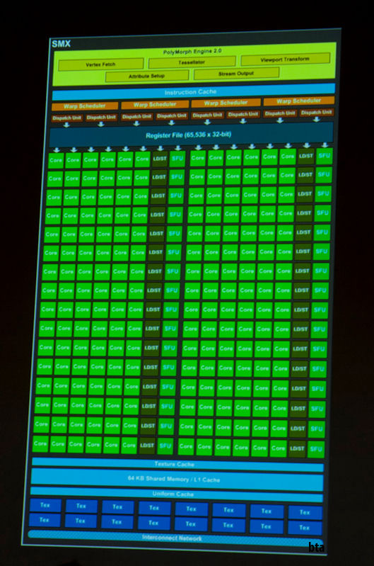 The specs of the GeForce GTX680 (Name not official Yet) were detailed by 3DCenter while Semiaccurate tells that the chip would be available in two variants.
The Specification shows that the Cuda Core Architecture would get a completely new design and would drop hot clocks being featured on previous generation cards. The Top GK-104 chip would be known as the GTX680/780 and would be manafactured using TSMC’s 28nm Fabrication Process.
GK-104 would pack 96 Stream Processors per cluster totaling at around 1536 Cuda Cores, 128 Texture Units, 32 ROP’s and a 2048Mb GDDR5 memory as standard, Core clock frequency would be set at 950Mhz.
Nvidia Kepler GK-104:
|
 9 teraflops , double precision with 1:6 = 486 DP GFlops processing power, 121 Texture Rate Gtex/sec
The die size for both GK104 and GK110 have been revealed by Charlie on Semiaccurate which match the 3DCenter’s details. Semiaccurate has also release a new article which shows that the GK104 would be launched in two variants, GK104-400 and GK104-335 (Source). Such product codes were recently used on the Fermi based GTX560 and 560Ti cards where GTX560ti was marked GF114-400 and GTX560 was marked as GF114-325. This could suggest that specific GK104 based models would come with shader clusters disabled.
Other details include a 225W TDP and a price point of $299 for the performance segment cards, Performance is rumored to be faster than the AMD’s recently launched HD7970 Tahiti based card which is currently the fastest GPU on the planet!
Kepler is expected to launch in April 2012.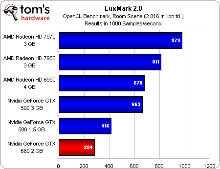
More details on Nvidia Kepler:
NVIDIA GeForce Kepler GK-104 Specifications Leaked, Features 256-bit Memory Bus and 225W TDP
Alleged NVIDIA GeForce GK-104 “Kepler” Specifications Leaked
Share this story
|
3DNews Technologies and IT market. News Rumors Specs NVIDIA GK104 GeForce GTX … The most interesting in the reviews
02/13/2012 [02:03], Konstantin Khodakovsky In recent weeks, there has been a flurry of rumors about the specifications of NVIDIA’s first 28nm graphics cards, codenamed Kepler. Many of them turned out to be fakes, but 3DCenter, followed by BSN, report that they have in their hands the full final specifications of the GK104 performance chip, which will form the basis of the GeForce GTX 680/670 cards.
Architecture diagram NVIDIA Kepler GK104: at first glance, it looks very similar to GF110, but if you look closely, the new chip offers 1536 stream processors instead of 512! It is reported that although initially NVIDIA wanted to call the card based on the GK104 chip the name GeForce GTX 660, later the choice was made in favor of the GTX 680 (it is indicated that 99% of the market name will be GK104). This card will be designed for the $350-400 market, and the performance of the accelerator will not only be higher than the GTX 580, Radeon HD 7950 3 GB for $450, but can even compete with the Radeon HD 7970 for $550.
Why? The fact is that the card will receive a new architecture with 1536 stream processors (or CUDA cores in NVIDIA’s terminology), which will be divided into 4 graphics computing clusters (GPCs) with four streaming multiprocessors (SMs) with 96 CUDA cores in each. Basic combinations of computing units of the NVIDIA Kepler family — 96 stream processors (1 SM), 384 (1 GPC), 768 (2 GPC), 1536 (4 GPC), 2304 (6 GPC). As reported, in addition to the GK104, a single-chip GeForce GTX 69 accelerator will also be released.0 with 2304 stream processors. Nothing is said about the dual-chip solution. Continuing talking about GK104, it should be noted that the card should get the same number of texture units and rasterization units as Tahiti XT — 128 TMU and 32 ROP. The card will rely on a 256-bit memory bus and, accordingly, 2 GB of video memory. The expected core frequency is 950 MHz (there is no separate frequency for shaders now), and, according to BSN, the frequency of 772 MHz will correspond in performance to approximately GTX 580, and 925 MHz — Tahiti XT. The memory frequency will be set to 1.25 GHz (5 GHz effective). In the area of bandwidth, therefore, the GTX 680 with its 160 GB/s will be inferior to the GTX 580 (192.4 GB/s), but will outperform the GTX 560 Ti (128. Other features of the GTX 680 include peak performance of 2.9 teraflops in single precision and 486 gigaflops in double precision. The area of the crystal will be about 340 square meters. mm. If the new rumors are true, then the GTX 680 will be a formidable rival to the Radeon HD 79 cards.00 at a lower cost. This is very reassuring. Related materials: Sources:
Permanent URL: https://3dnews.ru/624442 Headings: Tags: ← |
 27 GB/s).
 History of Nvidia Streaming Multiprocessors / Sudo Null IT News
I spent the last weekend learning CUDA and SIMT programming.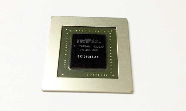 This fruitful time ended with an almost 700-fold acceleration of my “tracer on a business card” [1] — from 101 seconds to 150 ms.
Such an enjoyable experience was a good pretext for further exploration of the topic and the evolution of the Nvidia architecture. Thanks to the sheer volume of documentation published over the years by the green team, I was able to go back in time and briefly walk through the amazing evolution of their streaming multiprocessors.
In this article, we will review:
 Year Generation Series Crystal Manufacturing process The most powerful card
================================================= =========================
2006 Tesla GeForce 8 G80 90 nm 8800 GTX
2010 Fermi GeForce 400 GF100 40 nm GTX 480
2012 Kepler GeForce 600 GK104 28 nm GTX 680
2014 Maxwell GeForce 900 GM204 28nm GTX 980ti
2016 Pascal GeForce 10 GP102 16 nm GTX 1080 Ti
2018 Turing GeForce 20 TU102 12 nm RTX 2080 Ti
Dead End
Up until 2006, NVidia’s GPU architecture correlated with the [2] rendering API logical steps. The GeForce 7900 GTX, driven by the G71 chip, consisted of three parts dealing with vertex processing (8 blocks), fragment generation (24 blocks), and fragment merging (16 blocks).
Crystal G71. Notice the Z-Cull optimization, which discards a fragment that would not pass the Z-test.
This correlation forced the designers to guess the location of the bottlenecks in the conveyor to properly balance each of the layers. With the advent of another stage in DirectX 10 — the geometry shader, Nvidia engineers were faced with the difficult task of balancing the die without knowing how actively this stage would be used. It’s time for a change.
Tesla
Nvidia solved the problem of growing complexity with Tesla’s «unified» architecture, released in 2006.
The G80 crystal no longer had layer differences. Thanks to the ability to execute the vertex, fragment and geometric «kernel», the stream multiprocessor (Stream Multiprocessor, SM) replaced all previously existing blocks. Load balancing was done automatically by replacing the «core» performed by each SM depending on the requirements of the pipeline.
«In fact, we threw out the entire NV30/NV40 shader architecture and created a new one from scratch with a new general purpose processor architecture (SIMT) that also introduced new processor design methodologies.»
Jonah Alben (extremtech.com interview)
No longer capable of executing SIMD instructions, «shader units» became «cores» capable of executing one integer or one float32 instruction per clock. SM receives threads in groups of 32 called warps. Ideally, all threads of the same warp execute the same instruction at the same time, only for different data (hence the name SIMT). The Multi-threaded Instruction Unit (MT) deals with enabling/disabling threads in a warp if their instruction pointer (Instruction Pointer, IP) converges/rejects.
Two SFUs help you perform complex mathematical calculations such as inverse square root, sin, cos, exp, and rcp.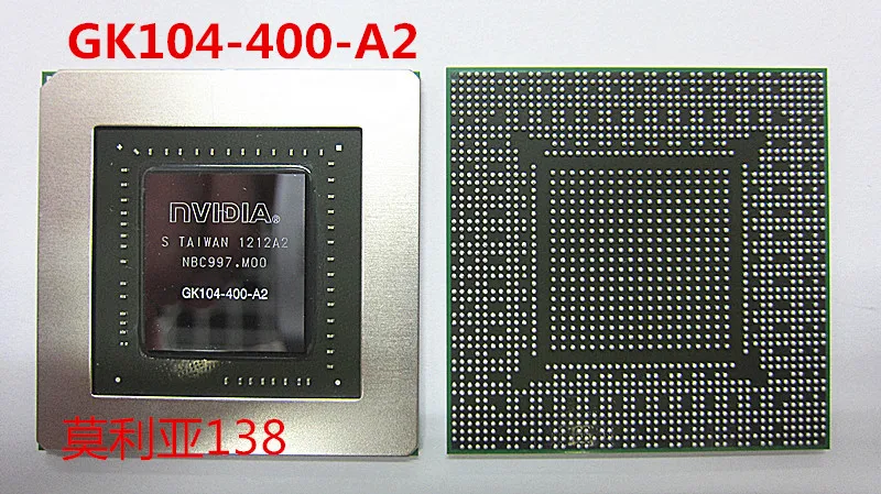 These blocks are also capable of executing one instruction per clock, but since there are only two of them, the speed of warp execution is divided by four. There is no hardware support for float64, the calculations are performed in software, which greatly affects the execution speed.
The SM reaches its maximum potential when it is able to hide memory latency due to the constant presence of dispatchable warps, but also when the warp thread is not diverted (control logic keeps it in the same instruction execution path). Thread states are stored in 4-kilobyte register files (Register File, RF). Threads that take up too much stack space reduce the number of possible threads that can run at the same time, reducing performance.
The flagship die of the Tesla generation was the 90nm G80 introduced in the GeForce 8800 GTX. The two SMs are combined into a Texture Processor Cluster (TPC) along with a Texture Unit and a Tex L1 cache. The G80, with 8 TPCs and 128 cores, was promised to generate 345.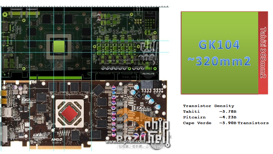 6 gigaflops [3] . The 8800 GTX card was hugely popular in its day, getting great reviews and loved by those who could afford it. It turned out to be such an excellent product that, thirteen months after its release, it remained one of the fastest GPUs on the market.
G80 installed in 8800 GTX. Render Output Units (ROP) are responsible for performing anti-aliasing.
Together with Tesla, Nvidia introduced the C programming language for Compute Unified Device Architecture (CUDA), a superset of the C99 language. This appealed to GPGPU enthusiasts, who welcomed the alternative to tricking the GPU with GLSL textures and shaders.
Although I’m mostly talking about SM in this section, it was only one half of the system. The SM needs to pass instructions and data stored in GPU memory. To avoid idle times, GPUs don’t try to minimize memory hits with large caches and predictions, as CPUs do. GPUs take advantage of latency by saturating the memory bus to meet the I/O needs of thousands of threads. To do this, a die (eg G80) implements high memory bandwidth using six double-sided DRAM memory buses.
GPUs take advantage of memory latencies while CPUs hide them with huge cache and prediction logic.
Fermi
Tesla was a risky move that turned out to be very successful. It was so successful that it became the foundation for NVidia’s GPUs for the next two decades.
“While we have certainly made major architectural changes since then (Fermi was a major system architecture change and Maxwell was another major change in processor design), the fundamental architecture we introduced with the G80 remains the same today [ Pascal].
Jonah Alben (extremtech.com interview)
In 2010, Nvidia released the GF100 based on the brand new Fermi architecture. The insides of her latest chip are detailed in the Fermi white paper [4] .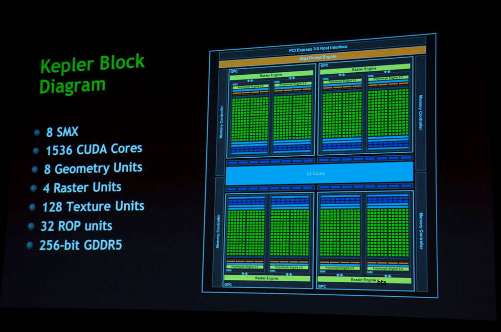
The execution model is still based on warps of 32 threads dispatched in SM. NVidia was able to double/quadruple all the numbers with the 40nm process technology alone. Thanks to two arrays of 16 CUDA cores, SM could now dispatch two half-warps (16 threads each) at the same time. With each core executing one instruction per clock, the SM was essentially able to eliminate one warp instruction per clock (four times as many as Tesla’s SM).
The number of SFUs has also increased, but not as much — the capacity has only doubled. It can be concluded that instructions of this type were not used very actively.
There is semi-hardware float64 support that combines the operations performed by the two CUDA cores. Thanks to the 32-bit ALU (Tesla used to have 24-bit ALU), the GF100 can perform an integer multiplication in one cycle, and due to the transition from IEEE 754-1985 to IEEE 754-2008, it has increased accuracy when working with a float32 pipeline using Fused Multiply -Add (FMA) (more accurate than that used in Tesla MAD).
From a programming standpoint, Fermi’s unified memory system allowed CUDA C to be extended with C++ features such as object, virtual methods, and exceptions.
With texture units now SM, the TPC concept has been abandoned. It has been replaced by Graphics Processor Clusters (GPCs) with four SMs. Lastly, SM is now gifted with the Polymorph Engine, which handles vertex acquisition, viewport transformation, and tessellation. The flagship GeForce GTX 480 card based on the GF100 was advertised as containing 512 cores and capable of delivering 1,345 gigaflops [5] .
GF100 installed in a GeForce GTX 480. Notice the six memory controllers serving the GPC.
Kepler
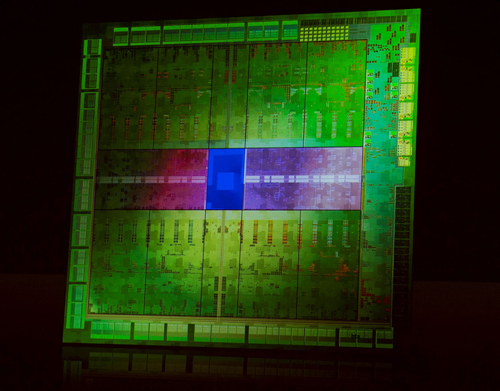
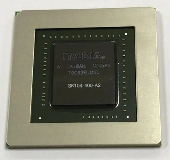
In 2012, Nvidia released the Kepler architecture, named after the astrologer best known for discovering the laws of planetary motion. As usual, the technical documentation GK104 [6] allowed us to look inside.
With Kepler, Nvidia has greatly improved the power efficiency of the die by lowering the clock speed and merging the core clock with the card clock (previously they were halved).
Such changes should have led to a decrease in performance. However, thanks to a halved process technology (28 nanometers) and the replacement of a hardware dispatcher with a software one, Nvidia was able not only to fit more SMs on the chip, but also to improve their design.
The Next Generation Streaming Multiprocessor (SMX) is a monster with nearly every performance doubled or tripled.
With four warp dispatchers capable of processing an entire warp in one cycle (Fermi could only process half a warp), SMX now contained 196 cores. Each dispatcher had dual dispatch, allowing the execution of a second instruction in a warp if it was independent of the currently executing instruction. Dual dispatch was not always possible because one column of 32 cores was shared between two dispatch operations.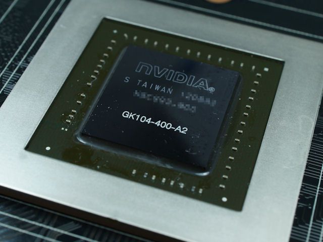
This scheme complicated the scheduling logic (we will return to this later), but due to the execution of up to six warp instructions per clock cycle, the SMX provided twice the performance compared to the SM of the Fermi architecture.
NVIDIA’s flagship GeForce GTX 680 with GK104 die and eight SMXs was claimed to have 1536 cores reaching 3250 gigaflops [7] . The elements of the crystal became so confusing that I had to remove all the labels from the circuit.
GK104 found in the GeForce GTX 680.
Check out the completely redesigned memory subsystems running at breathtaking 6 GHz. They allowed to reduce the number of memory controllers from six to four.
Maxwell
In 2014, Nvidia released the tenth generation GPU called Maxwell. As stated in the white paper GM107 [8] , the motto of the first generation of the architecture was «Maximum energy efficiency and extreme performance per watt consumed.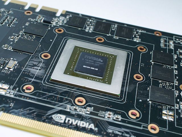 » The cards were marketed for «power-constrained environments such as laptops and small form factor (SFF) PCs.»
The most important decision was the abandonment of the Kepler structure with the number of CUDA cores in the SM that is not a power of two: some cores became shared and returned to work in half-warp mode. For the first time in the history of the SMM architecture, it had fewer cores than its predecessor: «only» 128 cores.
Matching the number of cores and warp size improved die segmentation, resulting in area and power savings.
One 2014 SMM had as many cores (128) as the entire GTX 8800 in 2006.
The second generation of Maxwell (described in the GM200 datasheet [9] ) has greatly improved performance while maintaining the energy efficiency of the first generation.
The process technology remained at 28nm, so Nvidia engineers could not resort to simple miniaturization to improve performance.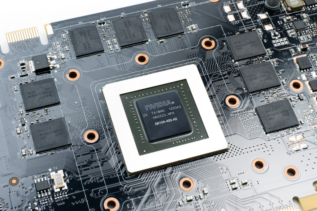 However, the reduction in the number of SMM cores reduced their size, allowing more SMMs to fit on the die. Compared to Kepler, the second generation of Maxwell doubled the amount of SMM, while increasing the die area by only 25%.
The list of enhancements also includes a simplified dispatch logic that reduces redundant dispatch recalculations and computation latency, resulting in more optimal use of warps. The memory frequency has also been increased by 15%.
Studying the block diagram of the Maxwell GM200 is already starting to strain your eyes. But we are still studying it closely. Flagship NVIDIA GeForce GTX 980 Ti with GM200 die and 24 SMM promised 3,072 cores and 6,060 gigaflops [10] .
GM200 installed in a GeForce GTX 980 Ti.
Pascal
In 2016, Nvidia introduced Pascal. Datasheet GP104 [11] leaves a feeling of déjà vu because the Pascal SM looks exactly like the Maxwell SMM.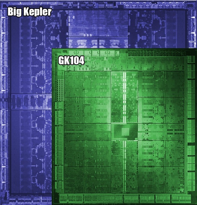 The lack of SM changes didn’t lead to performance stagnation because the 16nm process allowed more SMs to fit and double the gigaflops again.
Other major improvements included a memory system based on the all-new GDDR5X. The 256-bit memory interface, thanks to eight memory controllers, provided transfer rates of 10 gigaflops, increasing memory bandwidth by 43% and reducing warp idle time.
NVIDIA’s flagship GeForce GTX 1080 Ti with GP102 die and 28 TSM promised 3584 cores and 11,340 gigaflops [12] .
GP104 installed in GeForce GTX 1080.
Turing
With the release of Turing in 2018, Nvidia made its «biggest architectural leap forward in ten years» [13] . In Turing SM, not only specialized Tensor cores with artificial intelligence appeared, but also cores for ray tracing (rautracing, RT). This fragmented structure reminds me of the layered architecture that existed before Tesla, and it proves once again that history loves repetition.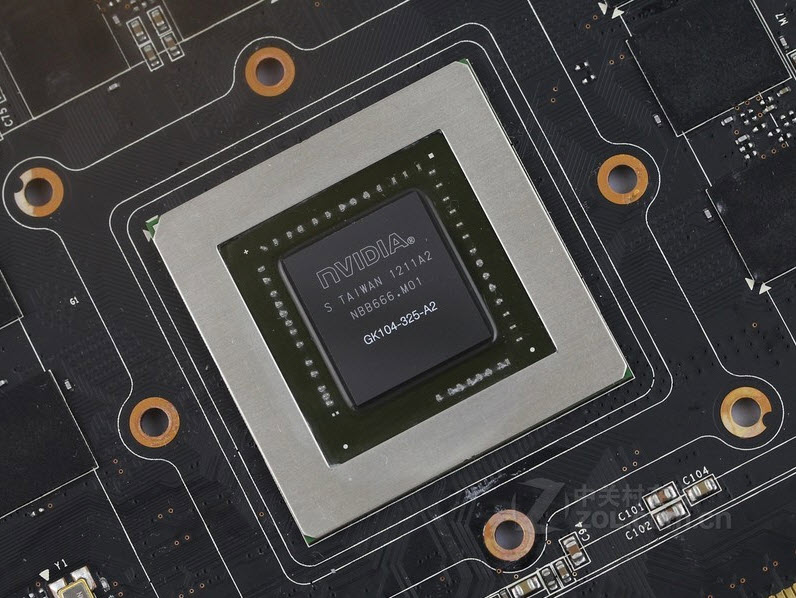
In addition to the new cores, Turing has three important features. First, the CUDA core has now become superscalar, which allows you to execute instructions with integers and floating point numbers in parallel. If you caught the year 1996, then this may remind you of Intel’s «innovative» Pentium architecture.
Secondly, the new GDDR6X memory subsystem, supported by 16 controllers, is now capable of providing 14 gigaflops.
Third, threads no longer have common instruction pointers (IP) in warp. Thanks to Volta’s Independent Thread Scheduling, each thread has its own IP. As a result, SMs are able to more flexibly configure warp thread scheduling without having to converge as quickly as possible.
NVIDIA’s flagship GeForce GTX 2080 Ti with TU102 die and 68 TSM has 4352 and goes up to 13 45 gigaflops [14] . I didn’t draw the block diagram because it would look like a blurry green spot.
What lies ahead for us
The next architecture, codenamed Ampere, is rumored to be announced in 2020.