The Cache Debate, LGA-1156 and the 32nm Future
by Anand Lal Shimpion November 19, 2008 8:00 PM EST
- Posted in
- CPUs
33 Comments
|
33 Comments
IndexMainstream Nehalem: On-chip GPU and On-chip PCIeWhat to Buy: Mainsteam vs. High End NehalemWhat’s Next: A Preview of Westmere and Sandy Bridge
Another Part? Oh there will be more
In an unexpected turn of events I found myself deep in conversation with many Intel engineers as well as Pat Gelsinger himself about the design choices made in Nehalem. At the same time, Intel just released its 2009 roadmap which outlined some of the lesser known details of the mainstream LGA-1156 Nehalem derivatives.
I hadn’t planned on my next Nehalem update being about caches and mainstream parts, but here we go. For further reading I’d suggest our first two Nehalem articles and the original Nehalem architecture piece.
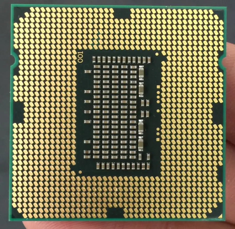
Nehalem’s Cache: More Controversial Than You’d Think
I spoke with Ronak Singhal, Chief Architect on Nehalem, at Intel’s Core i7 launch event last week in San Francisco and I said to him: “I think you got the cache sizes wrong on Nehalem”. I must be losing my shyness.
He thought I was talking about the L3 cache and asked if I meant it needed to be bigger, and I clarified that I was talking about the anemic 256KB L2 per core.
We haven’t seen a high end Intel processor with only 256KB L2 per core since Willamette, the first Pentium 4. Since then Intel has been on a steady ramp upwards as far as cache sizes go. I made a graph of L2 cache size per core of all of the major high end Intel cores for the past decade:
Click to Enlarge
For the most part we’ve got a linear trend, there are a few outliers but you can see that earlier in 2008 you’d expect Intel CPUs to have around 2 — 3MB of L2 cache per core. Now look at the lower right of the chart, see the little orange outlier? Yeah, that’s the Core i7 with its 256KB L2 cache per core, it’s like 2002 — 2007 never happened.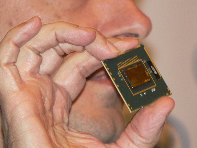
If we look at total on-chip cache size however (L2 + L3), the situation is very different:
Click to Enlarge
Now we’ve got an exponential growth of cache size, not linear, and all of the sudden the Core i7 conforms to societal norms. To understand why, we have to look at what happened around 2005 — 2006: Intel started shipping dual-core CPUs. As core count went up, so did the total amount of cache per chip. Dual core CPUs quickly started shipping with 2MB and 4MB of cache per chip and the outgoing 45nm quad-core Penryns had 12MB of L2 cache on a single package.
The move to multi-core chip designs meant that the focus was no longer on feeding the individual core, but making sure all of the cores on the chip were taken care of. It’s all so very socialist (oh no! 😉 ).
Nehalem was designed to be a quad-core product, but also one that’s able to scale up to 8 cores and down to 2 cores. Intel believes in this multi-core future so designing for dual-core didn’t make sense as eventually dual-core will go away in desktops, a future that’s still a few years away but a course we’re on nonetheless.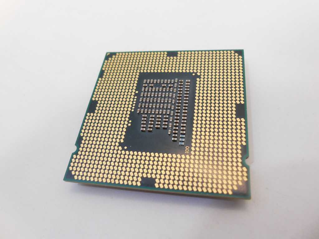
AMD’s shift to an all quad-core client roadmap
Intel is pushing the shift to quad-core, much like AMD is. By 2010 all of AMD’s mainstream and enthusiast CPUs will be quad-core with the ultra low end being dual-core, a trend that will continue into 2011. The shift to quad-core makes sense, unfortunately today very few consumer applications benefit from four cores. I hate to keep re-using this same table but it most definitely applies here:
Back when AMD introduced its triple-core Phenom parts I put together a little table illustrating the speedup you get from one, two and four cores in SYSMark 2007:
| SYSMark 2007 Overall | E-Learning | Video Creation | Productivity | 3D | |
Intel Celeron 420 (1 core, 512KB, 1.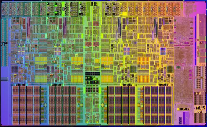 6GHz) 6GHz) |
55 | 52 | 55 | 54 | 58 |
| Intel Celeron E1200 (2 cores, 512KB, 1.6GHz) | 76 | 68 | 91 | 70 | 78 |
| % Increase from 1 to 2 cores | 38% | 31% | 65% | 30% | 34% |
Intel Core 2 Duo E6750 (2 cores, 4MB, 2.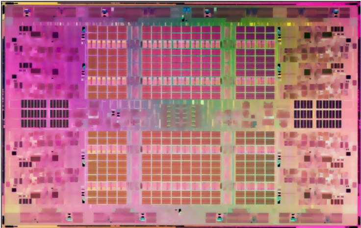 66GHz) 66GHz) |
138 | 147 | 141 | 120 | 145 |
| Intel Core 2 Quad Q6700 (4 cores, 8MB, 2.66GHz) | 150 | 145 | 177 | 121 | 163 |
| % Increase from 2 to 4 cores | 8.7% | 0% | 26% | 1% | 12% |
Not only are four cores unnecessary for most consumers today, but optimizing a design for four cores by opting for very small, low latency L2 caches and a large, higher latency L3 cache for the chip isn’t going to yield the best desktop performance.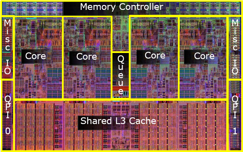
A Nehalem optimized for two cores would have a large L2 cache similar to what we saw happening on the first graph, but one optimized for four or more cores would look like what the Core i7 ended up being. What’s impressive is that Intel, in optimizing for a quad-core design, was still able to ensure that performance either didn’t change at all or improved in applications that aren’t well threaded.
Apparently the L2 cache size was and still is a controversial issue within Intel, many engineers still feel like it is too small for current workloads. The problem with making it larger is not just one of die size, but also one of latency. Intel managed to get Nehalem’s L2 cache down to 10 cycles, the next bump in L2 size would add another 1 — 2 cycles to its latency. At 512KB per core, 20% longer to access the cache was simply unacceptable to the designers.
In fact, going forward there’s no guarantee that the L2 caches will see growth in size, but the focus instead may be on making the L3 cache faster.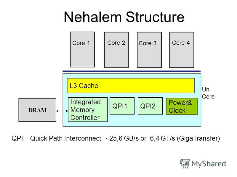 Right now the 8MB L3 cache takes around 41 cycles to access, but there’s clearly room for improvement — getting a 30 cycle L3 should be within the realm of possibility. I pushed Ronak for more details on how Intel would achieve a lower latency L3, but the best I got was “microarchitectural tweaks”.
As I mentioned before, Ronak wanted the L3 to be bigger on Nehalem; at 8MB that’s only 2MB per core and merely sufficient in his eyes. There are two 32nm products due out in the next 2 years, I suspect that at least one of them will have an even larger L3 to continue the exponential trend I showed in the second chart above.
Could the L2 be larger? Sure. But Ronak and his team ultimately felt that the tradeoff between size/latency was necessary for what Intel’s targets were with Nehalem. And given its 0 — 60% performance increase, clock for clock, over Penryn — I can’t really argue.
Mainstream Nehalem: On-chip GPU and On-chip PCIe
IndexMainstream Nehalem: On-chip GPU and On-chip PCIeWhat to Buy: Mainsteam vs.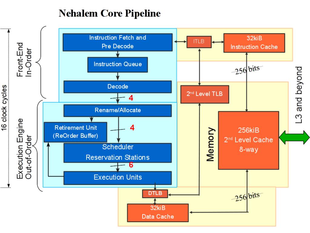 High End NehalemWhat’s Next: A Preview of Westmere and Sandy Bridge
PRINT THIS ARTICLE
Intel shows off 32nm chip, offers update on Penryn, Nehalem
Article Hero Image
AppleInsider may earn an affiliate commission on purchases made through links on our site.
Presenting at its Intel Developer Forum in San Francisco on Tuesday, Intel Corp. demonstrated the industry’s first 32-nanometer (nm) chip and also offered a status update on its upcoming «Penryn» family of processors and next-generation «Nehalem» architecture.
Chief executive Paul Otellini said chips based on its upcoming 32nm technology are due out in 2009 and will include transistors so small that more than 4 million of them could fit on the period at the end of this sentence. He also provided an overview of the advantages of the upcoming 45nm family of Penryn processors, which are based on the chipmaker’s high-k metal gate transistor technology and slated to ship this November.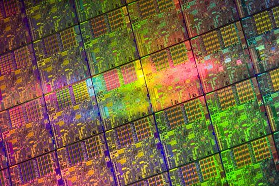
«Our tick-tock strategy of alternating next generation silicon technology and a new microprocessor architecture — year after year — is accelerating the pace of innovation in the industry,» said Otellini. «Tick-tock is the engine creating today’s most advanced technologies and keeps them coming out at a rapid cadence. Our customers and computer users around the world can count on Intel’s innovation engine and manufacturing capability to deliver state-of-the-art performance that rapidly becomes mainstream.»
Penryn
When Intel introduces Penryn in a few weeks, it will be the world’s first high-volume 45nm processor, the company said. Along with the Silverthorne family of 45nm processors due next year, Penryn will have the small feature size, low-power requirements and high-performance capabilities to meet a wide variety of computing needs from handheld Internet computers to high-end servers.
Intel, which already claims to have achieved more than 750 design wins for the Penryn processor, plans to quickly ramp the technology, introducing 15 new 45nm processors by the end of the year and another 20 in the first quarter of 2008.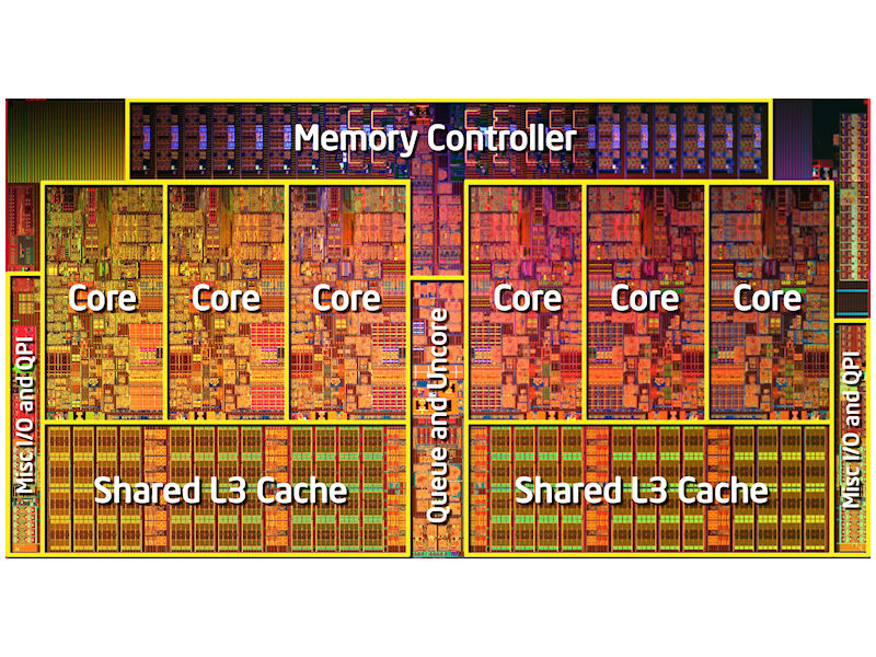
«We expect our Penryn processors to provide up to a 20 percent performance increase while improving energy efficiency,» he said. «Intel’s breakthrough 45nm silicon process technology allows us to provide low-cost, extremely low-power processors for innovative small form factor devices while delivering high-performance, multi-core, multi-featured processors used in the most advanced systems.»
Otellini also announced that Intel’s 45nm processors and 65nm chipsets would use halogen-free packaging technology beginning next year, yielding chips that will not only be more energy efficient but also better for the environment.
Nehalem
Looking to 2008, the Intel chief also conducted the first public demonstration of Intel’s Nehalem processor and said the company is on track to deliver the new processor design in the second half of the year.
The Nehalem architecture was conceived with the company’s leadership in performance-per-watt in mind, and will give way to the first chip to utilize Intel’s QuickPath Interconnect system architecture, which includes integrated memory controller technology and improved communication links between system components to significantly improve overall system performance.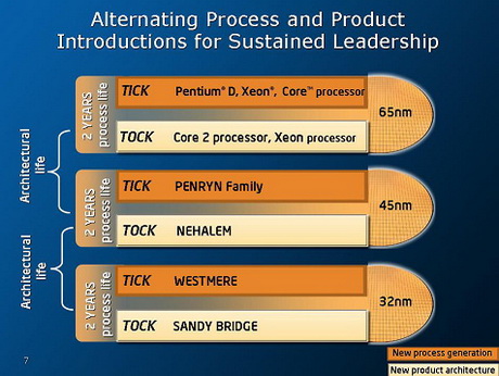
«Nehalem is an entirely new architecture that leverages Intel’s Core Microarchitecture, bringing leading-edge performance advantages, power efficiency and important new server features to market just a year after Intel leads the industry to 45nm technology,» said Otellini.
32nm technology
Describing other advanced Intel technologies destined to quickly come to market, Otellini showed the world’s first 300mm wafer built using next-generation 32nm process technology. The development of advanced test chips serves as a critical milestone in the company’s march toward high-volume manufacturing of 32nm process technology, which it plans for 2009.
Intel’s 32nm test chips incorporate logic and memory (static random access memory — SRAM) to house more than 1.9 billion transistors, Otellini said. The 32nm process also uses the company’s second-generation high-k and metal gate transistor technology.
This additional performance made possible by Intel’s push to drive chip design and manufacturing technology forward will not only be seen in computing, but will enable more true-to-life entertainment and realistic graphics capabilities. As a result, the company said it will be placing increased emphasis on using the power of its processors to enhance key technologies such as visual computing and graphics.
«Satisfying demand for ever-greater computer performance increases means we need to move rapidly to the next manufacturing technology.» said Otellini. «Intel engineers and researchers deserve a great deal of credit for setting the pace for the industry. As our advanced technology reaches consumers and businesses in the next couple of years the amount of computing power they’ll be able to harness will help them become even more productive, creative and innovative.»
25 watt Penryn
During his presentation, Otellini also announced that a version of a Penryn dual-core processor operating at 25 watts will be available on the upcoming Montevina platform, which will include Intel’s mobile WiMAX silicon. He said several equipment manufacturers are already planning to introduce Montevina-based notebook PCs starting next year when the platform is introduced.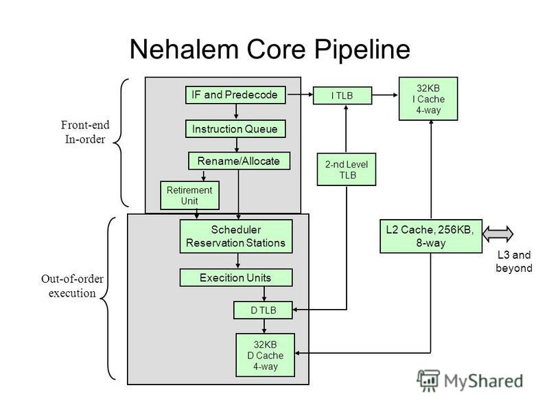
New details on 32nm Sandy Bridge processors
The first Intel processors with the Nehalem architecture will appear later this year. Thus, for the «Japanese soothsayers» this is already an almost worked out topic, and they will return to it only in case of emergency. Westmere processors, which will be produced in 32 nm technology from the beginning of 2010, will retain the Nehalem architecture, and only the process technology will be new. And only at the end of 2010, Sandy Bridge processors can appear, carrying a new architecture.
The Japanese site PC Watch has published a new article about the differences between Nehalem and Sandy Bridge processors from the current ones. The material uses both the statements of Intel representatives and information from some sources close to the manufacturers.
Let’s start with the fact that server-class Nehalem processors promise to demonstrate a significant performance increase over 45 nm Clovertown processors operating at 3. 0 GHz. For example, in the SPECint_rate2006 test, performance in integer operations will increase by 1.6 times, and in the SPECfp_rate2006 test, performance in floating point operations will increase by 2.4 times. The speed of interaction between processors will increase due to the rejection of the classic FSB in favor of the QPI serial bus, and the memory controller will benefit from being transferred directly to the processor.
Sandy Bridge generation processors are being developed by an Israeli engineering team, which at one time determined Intel’s success in the mobile segment with Pentium M processors. The American development team is preparing for the announcement of Nehalem. Such a parallel development scheme allows for a declared schedule of announcements, according to which a new architecture is presented every two years. It usually takes much longer to develop a new processor.
We should also return to the topic of integrating the graphics core into the processor, which was covered by Japanese colleagues last week. Then it was suggested that Nehalem processors would combine graphics and processor cores in one package, but physically these components would be placed on separate crystals. And only 32 nm followers will receive a graphics core on a monolithic crystal.
Israeli developers share the point of view that the graphics core should be placed on the same chip with the processor. The multi-chip layout does not provide visible advantages, according to the developers of Sandy Bridge, this is not much of an innovation. There is every chance that 32 nm Sandy Bridge processors will receive an integrated graphics core on a common chip with processors.
True, there are some obstacles here. The update cycle for graphics cores usually does not exceed 6 months, and the processor architecture is preparing for the announcement much longer. Thus, by the time a processor with a monolithic crystal is announced, its graphics core may be hopelessly outdated. To avoid this, Israeli engineers can use a processor architecture with a ring bus, as in Cell processors.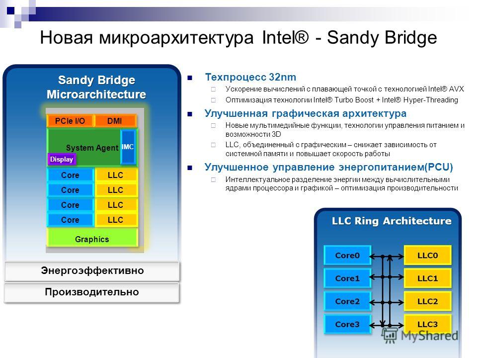 This will make it quite easy to integrate a modern graphics core into the processor or increase the number of main cores without significant design redesign.
Incidentally, Intel denies all accusations that it is copying AMD’s idea of creating a processor with an integrated graphics core. Representatives of the company say that Timna could have become the first hybrid processor if its development had not been curtailed at one time. This happened due to problems with the expediency of integrating a memory controller that was supposed to support RDRAM — this type of memory was too expensive.
recommendations
It remains to be hoped that Sandy Bridge processors will conquer the success of their mobile predecessors, which once left the doors of the Israeli laboratories of Intel. We just need to be patient until 2010.
Intel completed development of 32nm technology
Business
Digitization
Infrastructure
|
Share
Intel has completed the development of 32nm processor technology. The company reported that the release of the first chips based on it is expected on time — in the 4th quarter of 2009which once again proves the viability of the «tick-tock» strategy.
Intel Corporation announced the successful completion of research work on the introduction of a new technological process with a transistor size of 32 nm. The company will begin production of the first chips based on this technology in the 4th quarter of 2009, as previously planned. This was reported in a press release.
The technical features of the new processors will be presented at the IEDM, an international conference in the field of electronic devices, which will be held next week in San Francisco. Research papers describe high-k + metal gate transistor design technology and applications 193 nm immersion lithography.
In case of successful transition to 32-nm process technology in 2009, the corporation will once again prove the viability of the «tick-tock» strategy. This is a strategy that Intel has been pursuing since 2006, whereby after the previous generation architecture (tick) workflow has been reduced, a new architecture (tock) emerges. In this case, «tick» and «tock» occur sequentially every year. So, in 2008, a new microprocessor architecture Nehalem was introduced, in 200932-nm topology is expected to be introduced, and in 2010 the launch of a new architecture called Sandy Bridge. In 2011, it is planned to reduce transistors to 22 nm and so on. Currently, Intel processors (Nehalem architecture, as well as the previous one — Penryn) have a 45-nm topology.
New microprocessor architecture Nehalem introduced in 2008
Other chipmakers are also working on the introduction of 32 nm and have even formed an alliance to successfully achieve their goals. It includes IBM, Toshiba, AMD, Samsung, Infineon, Freescale and other well-known companies. The work of the group will last until 2010.