Pentium? Core i5? Core i7? Making sense of Intel’s convoluted CPU lineup
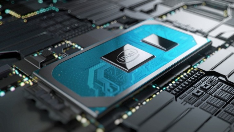
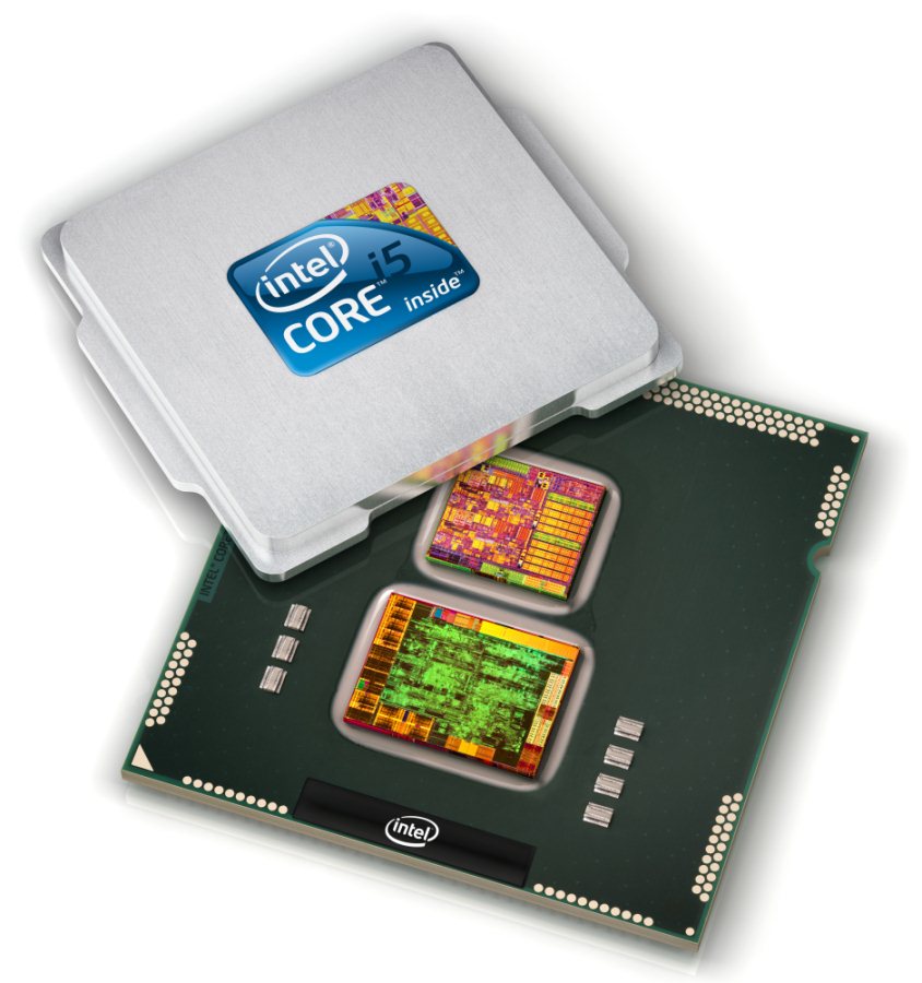
Enlarge / Intel’s Skylake-based Pentium G4500.
Andrew Cunningham
Our creative director Aurich Lawson is building a PC to power a custom arcade cabinet, and he was having trouble picking a processor. Not because he didn’t know what he needed, but because he was having trouble matching what he needed (the cheapest quad-core CPU that meets the recommended requirements for Street Fighter V) with what Intel was offering (five different obfuscated brands spread out over multiple sockets and architectures).
And if you’re building a PC now after having been out of the game for a few years, it can be exceptionally confusing. Around the turn of the millennium you just had Celeron and Pentium. One name meant “cut-down low-end” and one meant “high-end, more features,” and you just bought the fastest one you could reasonably afford. Things got a little more confusing in the Core and Core 2 days (the Core branding continues to survive alongside the Celeron and Pentium brands), but you could at least use names like “Core Solo” and “Core 2 Quad” to guess which architecture and how many cores you were getting. Now there are three separate Core brands, Pentium and Celeron brands, and a long series of letters that you need to know to figure out what CPU you’re getting.
It’s been a few years since the last time we demystified Intel’s CPU lineup, and in truth things haven’t changed too much. In broad strokes, the rules are the same. But Intel has introduced and retired a few CPU architectures and brands since then. We’ll run down the basics for both desktops and laptops to help you make some sense of things whether you’re building a computer or buying one from someone else.
First: Know your architectures
Right this second we’re in a sort of transitional phase where some old CPUs are still filtering out as new ones filter in. In brief:
Advertisement
The old chips, codenamed Haswell, are generally identifiable by their 4000-series model numbers or the “4th generation Core” label. The desktop chips use socket 1150 motherboards.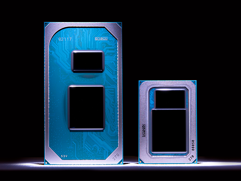 In general, we would recommend against considering these for new builds or purchases unless you can get a really good deal—Haswell is at the end of its life and Intel won’t be making new chips for its socket in the future. There are also a handful of 5000-series, 5th-generation Broadwell desktop chips that use the same socket—Intel didn’t do a full release of these CPUs because of manufacturing delays, so you’ll find the majority of them in laptops instead.
The new chips, codenamed Skylake, have 6000-series model numbers and a “6th generation Core” label. The desktop chips use socket 1151 motherboards, which is likely (not guaranteed, but likely) to see additional use in the upcoming Kaby Lake and Cannonlake architectures later this year and into next year. If you care at all about future-proofing, the small price premium is worth paying if you’re building a desktop.
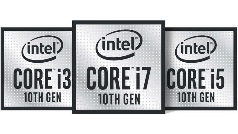
Desktops: Celeron, Pentium, and Core
There are a total of five separate processor brands that all share the Skylake architecture and the socket. I’ll list the high-level differences of each along with exceptions, and then we’ll get into model number suffixes.
Celerons and Pentiums
Both of these are budget brand names, and processors in both lines tend to be differentiated by clock speed and not much else. Skylake Pentiums are G4000-series chips, while Celerons are G3000-series. They’re all dual-core CPUs with no Turbo Boost, no Hyperthreading, and 3MB of cache, and they’re typically paired with the basic Intel HD 510 integrated GPU.
Core i3 CPUs are a little faster, but Pentiums will give most price-conscious people the best bang for their buck.
Exceptions: The Pentium G4500-series chips get an Intel HD 530 GPU that’s quite a bit faster than the 510 (within the realm of integrated graphics, anyway).
Core i3
These CPUs are still dual-core but add Hyperthreading, which presents two logical processor cores to the operating system for every physical core. This can definitely help performance in multithreaded workloads, though it’s nowhere near the boost you’d get from moving to a quad-core CPU. Core i3-6100 CPUs include 3MB of cache while 6300-series chips include 4MB of cache; nearly all of them use the Intel HD 530 GPU.
Advertisement
Exceptions: The Core i3-6098P uses an Intel HD 510 GPU.
Core i5
These are all quad-core CPUs without Hyperthreading, and they probably represent the best balance of price and performance for high-end users. They also use Intel’s Turbo Boost feature, which let the CPU run at higher clock speeds when there’s enough thermal headroom or when fewer cores are being actively used.
Not all workloads will benefit from two extra processor cores, but video editing, Photoshop work, and an increasingly large number of games are all happier with four cores. All of these CPUs include 6MB of cache and most of them have Intel HD 530 GPUs.
Exceptions: The Core i5-6402P includes an Intel HD 510 GPU.
Core i7
These are best described as Core i5 chips with Hyperthreading, higher clock speeds, and and 8MB of cache. Otherwise they’re the same. As with Core i3 CPUs, Hyperthreading definitely does help performance in heavily threaded programs, but jumping from a Pentium or Core i3 to a Core i5 will get you a much larger performance bump than jumping from an i5 to an i7.
Exceptions: None. There aren’t many of these processors yet.
Desktop Processor suffixes
The Celeron, Pentium, and various Core labels tell you most of what you need to know about a given CPU, but the model number suffix is important too. Here’s what these suffixes mean (and note that some CPUs have more than one letter attached).
No suffix: These are “mainstream” CPUs with no particularly special properties.
T-series: These are low-power desktop chips with lower TDP values, which generally (but not always) translates into lower power consumption. These power savings are usually realized by reducing the CPUs’ maximum clock speed. For example, a Core i7-6700 has a TDP of 65W, a base frequency of 3.4GHz, and a Turbo frequency of 4.0GHz. A Core i7-6700T has a TDP of 35W, a base frequency of 2.8GHz, and a max clock speed of 3.6GHz.
K-series: This relatively rare suffix denotes a multiplier-unlocked CPU that can be overclocked when paired with a high-end Intel Z170 chipset. The chips also have a higher 91W TDP, relative to the standard 65W for a quad-core CPU.
E-series: E is for “embedded,” which implies that these are mostly going to come with pre-built systems or soldered to motherboards. System builders can mostly ignore this one.
P-series: Back in the Core 2 days, a P-series chipset didn’t include an integrated GPU. Now, P-series chips just include slower integrated GPUs. Go figure.
Pentium 5, the processor that could not be
I still remember the surprise with which I received the arrival of Intel Pentium processors, back in 1993 (when I still aspired to buy a 386). It was for many reasons, of course, but there is one that I remember anecdotally, and that is that until they were announced, I expected the next generation to be… I’m sure you’ve guessed it, yes, 80586 or i586. Intel actually left this nomenclature behind in order to be able to commercially register the name (something that could not be done with numerical sequences).
Four years later, in 1997, the jump to Pentium II would arrive, which meant the abandonment (temporary, as we saw later) of the classic chip format inserted in a socket for a cartridge designed to improve heat dissipation, which was connected to the motherboard through a slot. It didn’t last long two years later came Pentium III that recovered the classic chip-in-socket format that has prevailed until today.
In those days, Intel was already very fast when it came to jumping from one generation to the next, so just a year later, At the end of 2000, the first Pentium 4 debuted on the market. So what could we expect at that time? Obviously, of course, that in 2001 (or at the latest in 2002) the new generation would arrive, which would obviously be Pentium 5, right? Well, it was expected, but as you probably already know, it is not what happened.
Intel Pentium 4 Prescott. Performance, yes, but at what thermal price… Image: JulianVilla26
Instead, Pentium 4 brought together, over the years, several different architectures: Willamette, Northwood, Northwood (Extreme Edition) and Prescott. Why did Intel decide not to increment the number at each of these jumps? There are some theories about it, such as the one that, erroneously, and due to the speed with which it jumped from version to version between Pentium and Pentium 4, there were users who thought that the number was a performance rating system, not a generation indicator.
Be that as it may, the point is that The Pentium 4 Prescott, released in early 2004, was already facing some high power issues and, directly associated, heat generation.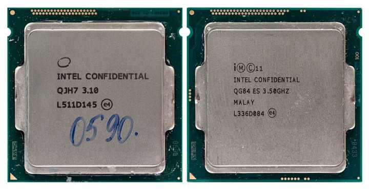 The top of the range of its generation was the Pentium 4 570J at 3.8 gigahertz, although Intel initially planned more powerful models, four gigahertz or more, finally the aforementioned problems made it impossible.
And then came 2006 but, contrary to expectations, a new Pentium 4 architecture or, more expected still, the leap to Pentium 5 did not come from it. Instead, Intel formulated a paradigm shift that, with time, has proven more than successful. I am referring, of course, to the production of processors with more than one core. Intel Core Duo had just been born, a design with two execution cores. The rest? Surely you already know it, first the addition of more higher performance cores in each generation of Intel Core up to the eleventh, and the jump to hybrid architecture with Alder Lake.
And what happened to the Pentium 5?
Now what happened? Why did Intel abandon Pentium and make the jump to multicore architecture? A video recently published on the Fully Buffered YouTube channel reminds us of some already known facts, and tells us some very interesting ones about Intel’s plans regarding the Pentium 5and why it never finally saw the light of day, in addition to showing us two chips from that lost generation and having a first-hand testimony about them.
The first thing to note is that yes, Intel had planned the jump from Pentium 4 to Pentium 5a chip that should have reached the spectacular speed of 7 gigahertz. Let us remember, for context, that the Intel Core i9-12900K has a maximum speed of 5.2 gigahertz, and we are talking about a processor, the Pentium 5, which would have hit the market around 15 years earlier. Those were the times of brute force and, although there was already talk of execution threads and others, the competition was determined by speed, rather than performance.
However, with Prescott Intel he encountered a wall, perhaps not insurmountable, but terribly complex, that of temperature which, as we have already mentioned, prevented this generation from reaching the speeds initially planned.
Now, more than a year before the arrival on the market of the Pentium 4 Prescott, Intel had already started work on two architectures, called Texas and Jayhawk. The first would be the successor to Prescott and the one that would mark the jump to Pentium 5, while Jayhawk would mark the generational jump of Intel Xeon. Intel had already anticipated in 2003, showing a preliminary design, that Texas would reach the market in 2004, although later it was delayed until 2005, before cancel both projects in May 2004.
Steve Fischer, one of the Intel engineers who worked on the Texas and Jayhawk projects, with whom Fully Buffered spoke, has revealed in that video quite a bit of additional information about the project, about the challenges they faced and about the reasons that finally pushed Intel to back down, to abandon the gigahertz race (its initial goal was to reach 10 gigahertz in 2011), focusing on performance… although without forgetting speed.
After the cancellation of the Pentium 5, Intel opted for the multicore that debuted in the Core Duo, which in turn found its continuation in the Core 2 Duo, predecessor of the current Intel Core.
Fischer says that the thermal problem was decisive. At that time the fastest processor in the house reached, as we have mentioned before, 3.8 gigahertz, and for this its TDP was 115 watts. Thus, and with that technology, andscaling up to 7 gigahertz would have resulted in increasing the TDP to around 250 watts, probably something else. I know this doesn’t seem like much today (the TDP of the Core i9-12900K in turbo mode is 241 watts), but we’re talking about almost 20 years ago, processors with a 90 nanometer lithography (Although eventually the jump was made to 65 nanometers).
I called this thing “the Death Star of processors” and half-jokingly reasoned that consumer acceptance of liquid-cooled chassis wouldn’t be a big deal.
A TDP of 250 watts was, in those days, something simply monstrous for a desktop system and, although liquid cooling solutions already existed, they were still extremely rare and quite expensive, that is, they were not an option that Intel could consider.
Canceling Texas and Jayhawk was certainly not an easy decision, as involved making a complex leap to an architecture with more than one core and, in addition, to give up the milestone of 10 gigahertz, a key element in its competition, in those days, with AMD. But, after analyzing all the possibilities, the engineering teams involved in the project concluded that they faced a dead end.
As we remembered before, this “stumble” gave rise to a paradigm shift inaugurated with Intel Core Duoand that has brought us to the point where we are now, waiting for the arrival of the Intel Core i9-13900K, with its 24 cores (8 for performance and 16 for efficiency) and its consequent 32 threads, and that already It has been seen touching 6. 1 gigahertz.
A) Yes, the Pentium 5 never reached the market but it did exist, and some silicons were even produced, such as the one obtained by the creator of the video. And perhaps if Intel engineers had found a solution to the power and heat problem, today’s processors would be very different. Of course, if two engineering teams, with the means available at the time, determined that it was not possible, we do not have much room for imagination.
Intel Core i5-8305G vs Intel Pentium Gold 5405U: What is the difference?
54points
Intel Core i5-8305G
41points
Intel Pentium Gold 5405U
Comparison winner
vs
64 facts in comparison
Intel Core i5-8305G
Intel Pentium Gold 5405U
Why is Intel Core i5-8305G better than Intel Pentium Gold 5405U?
- 2.43x faster CPU speed?
4 x 2.8GHzvs2 x 2.3GHz - 267MHz higher ram speed?
2400MHzvs2133MHz - 4 more CPU threads?
8vs4 - 631MHz faster GPU clock speed?
931MHzvs300MHz - 0.
 5MB bigger L2 cache?
1MBvs0.5MB - 3.18x higher PassMark result?
7231vs2276 - 4MB bigger L3 cache?
6MBvs2MB - 1 newer version of PCI Express (PCIe)?
3vs2
Why is Intel Pentium Gold 5405U better than Intel Core i5-8305G?
- 50W lower TDP?
15Wvs65W
Which are the most popular comparisons?
AMD Ryzen 5 5500U
vs
Intel Core i5-1135G7
AMD Ryzen 3 3250U
vs
Intel Core i3-1115G4
AMD Ryzen 3 5300U
vs
Intel Core i3-1115G4
AMD Ryzen 7 3700U
vs
Intel Core i5-10210U
AMD Ryzen 7 3700U
vs
Intel Core i5-1135G7
AMD Ryzen 5 4600H
vs
Intel Core i5-10300H
Intel Core i3-1115G4
vs
Intel Core i5-10210U
AMD Ryzen 5 3500U
vs
Intel Core i5-10210U
AMD Ryzen 5 5500U
vs
Intel Core i3-1115G4
AMD Ryzen 7 5800H
vs
Intel Core i7-11800H
Price comparison
User reviews
Overall Rating
Intel Core i5-8305G
0 User reviews
Intel Core i5-8305G
0. 0/10
0/10
0 User reviews
Intel Pentium Gold 5405U
3 User reviews
Intel Pentium Gold 5405U
7.3/10
3 User reviews
Features
Value for money
No reviews yet
7.0/10
3 votes
Gaming
No reviews yet
7.0/10
3 votes
Performance
No reviews yet
7.0/10
3 votes
Reliability
No reviews yet
7.0/10
3 votes
Energy efficiency
No reviews yet
7.0/10
3 votes
Performance
1.CPU speed
4 x 2.8GHz
2 x 2.3GHz
The CPU speed indicates how many processing cycles per second can be executed by a CPU, considering all of its cores (processing units). It is calculated by adding the clock rates of each core or, in the case of multi-core processors employing different microarchitectures, of each group of cores.
2. CPU threads
More threads result in faster performance and better multitasking.
3.turbo clock speed
3.8GHz
Unknown. Help us by suggesting a value. (Intel Pentium Gold 5405U)
When the CPU is running below its limitations, it can boost to a higher clock speed in order to give increased performance.
4.Has an unlocked multiplier
✖Intel Core i5-8305G
✖Intel Pentium Gold 5405U
Some processors come with an unlocked multiplier which makes them easy to overclock, allowing you to gain increased performance in games and other apps.
5.L2 cache
A larger L2 cache results in faster CPU and system-wide performance.
6.L3 cache
A larger L3 cache results in faster CPU and system-wide performance.
7.L1 cache
A larger L1 cache results in faster CPU and system-wide performance.
8.L2 core
0.25MB/core
0.25MB/core
More data can be stored in the L2 cache for access by each core of the CPU.
9.L3 core
1.5MB/core
1MB/core
More data can be stored in the L3 cache for access by each core of the CPU.
Memory
1.RAM speed
2400MHz
2133MHz
It can support faster memory, which will give quicker system performance.
2.maximum memory bandwidth
37.5GB/s
37.5GB/s
This is the maximum rate that data can be read from or stored into memory.
3.DDR memory version
Unknown. Help us by suggesting a value. (Intel Pentium Gold 5405U)
DDR (Double Data Rate) memory is the most common type of RAM. Newer versions of DDR memory support higher maximum speeds and are more energy-efficient.
4. memory channels
More memory channels increases the speed of data transfer between the memory and the CPU.
5.maximum memory amount
The maximum amount of memory (RAM) supported.
6.bus transfer rate
The bus is responsible for transferring data between different components of a computer or device.
7.Supports ECC memory
✖Intel Core i5-8305G
✖Intel Pentium Gold 5405U
Error-correcting code memory can detect and correct data corruption. It is used when is it essential to avoid corruption, such as scientific computing or when running a server.
8.eMMC version
Unknown. Help us by suggesting a value. (Intel Core i5-8305G)
Unknown. Help us by suggesting a value. (Intel Pentium Gold 5405U)
A higher version of eMMC allows faster memory interfaces, having a positive effect on the performance of a device. For example, when transferring files from your computer to the internal storage over USB.
9.bus speed
Unknown. Help us by suggesting a value. (Intel Core i5-8305G)
Unknown. Help us by suggesting a value. (Intel Pentium Gold 5405U)
The bus is responsible for transferring data between different components of a computer or device.
Benchmarks
1.PassMark result
This benchmark measures the performance of the CPU using multiple threads.
2.PassMark result (single)
This benchmark measures the performance of the CPU using a single thread.
3.Geekbench 5 result (multi)
Unknown. Help us by suggesting a value. (Intel Pentium Gold 5405U)
Geekbench 5 is a cross-platform benchmark that measures a processor’s multi-core performance. (Source: Primate Labs, 2022)
4.Cinebench R20 (multi) result
Unknown. Help us by suggesting a value. (Intel Core i5-8305G)
Unknown. Help us by suggesting a value. (Intel Pentium Gold 5405U)
Cinebench R20 is a benchmark tool that measures a CPU’s multi-core performance by rendering a 3D scene.
5.Cinebench R20 (single) result
Unknown. Help us by suggesting a value. (Intel Core i5-8305G)
Unknown. Help us by suggesting a value. (Intel Pentium Gold 5405U)
Cinebench R20 is a benchmark tool that measures a CPU’s single-core performance by rendering a 3D scene.
6.Geekbench 5 result (single)
Unknown. Help us by suggesting a value. (Intel Pentium Gold 5405U)
Geekbench 5 is a cross-platform benchmark that measures a processor’s single-core performance. (Source: Primate Labs, 2022)
7.Blender (bmw27) result
Unknown. Help us by suggesting a value. (Intel Core i5-8305G)
Unknown. Help us by suggesting a value.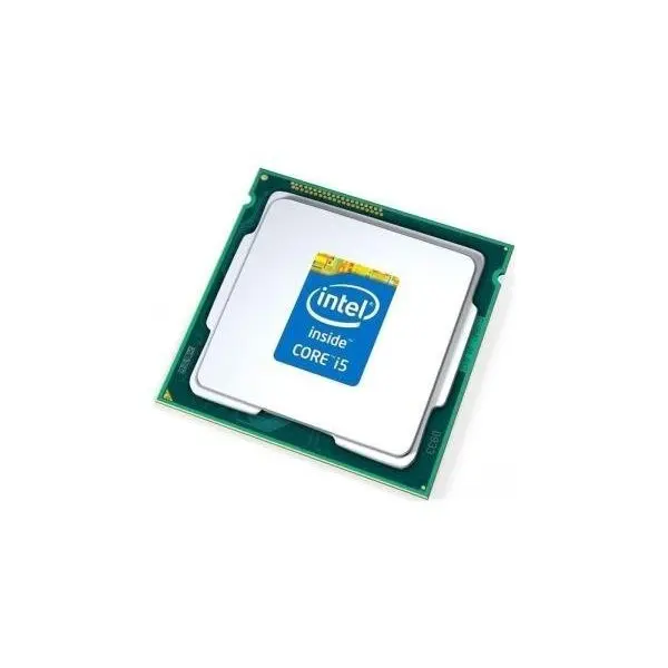 (Intel Pentium Gold 5405U)
The Blender (bmw27) benchmark measures the performance of a processor by rendering a 3D scene. More powerful processors can render the scene in less time.
8.Blender (classroom) result
Unknown. Help us by suggesting a value. (Intel Core i5-8305G)
Unknown. Help us by suggesting a value. (Intel Pentium Gold 5405U)
The Blender (classroom) benchmark measures the performance of a processor by rendering a 3D scene. More powerful processors can render the scene in less time.
9.performance per watt
Unknown. Help us by suggesting a value. (Intel Pentium Gold 5405U)
This means the CPU is more efficient, giving a greater amount of performance for each watt of power used.
Features
1.uses multithreading
✔Intel Core i5-8305G
✔Intel Pentium Gold 5405U
Multithreading technology (such as Intel’s Hyperthreading or AMD’s Simultaneous Multithreading) provides increased performance by splitting each of the processor’s physical cores into virtual cores, also known as threads. This way, each core can run two instruction streams at once.
2.Has AES
✔Intel Core i5-8305G
✔Intel Pentium Gold 5405U
AES is used to speed up encryption and decryption.
3.Has AVX
✔Intel Core i5-8305G
✖Intel Pentium Gold 5405U
AVX is used to help speed up calculations in multimedia, scientific and financial apps, as well as improving Linux RAID software performance.
4.SSE version
SSE is used to speed up multimedia tasks such as editing an image or adjusting audio volume. Each new version contains new instructions and improvements.
5.Has F16C
✔Intel Core i5-8305G
✖Intel Pentium Gold 5405U
F16C is used to speed up tasks such as adjusting the contrast of an image or adjusting volume.
6.bits executed at a time
Unknown. Help us by suggesting a value. (Intel Core i5-8305G)
Unknown. Help us by suggesting a value. (Intel Pentium Gold 5405U)
NEON provides acceleration for media processing, such as listening to MP3s.
7.Has MMX
✔Intel Core i5-8305G
✔Intel Pentium Gold 5405U
MMX is used to speed up tasks such as adjusting the contrast of an image or adjusting volume.
8.Has TrustZone
✖Intel Core i5-8305G
✖Intel Pentium Gold 5405U
A technology integrated into the processor to secure the device for use with features such as mobile payments and streaming video using digital rights management (DRM).
9.front-end width
Unknown. Help us by suggesting a value. (Intel Core i5-8305G)
Unknown. Help us by suggesting a value. (Intel Pentium Gold 5405U)
The CPU can decode more instructions per clock (IPC), meaning that the CPU performs better
Price comparison
Cancel
Which are the best CPUs?
Difference Between Intel Pentium vs i5
Intel Pentium and Intel Core i5 are in a completely different performance price categories. They are so further apart in terms of differences that a simple comparison is simply ridiculous. Yet, more often than not, those who are completely new to PC hardware often ask about the differences between Intel Pentium vs i5.
Simply put, Intel Pentiums are entry level CPUs whereas an Intel Core i5 is a mainstream CPU. The current generation of Intel Pentium CPUs offer 2 cores, whereas, the current generation of Intel Core i5 offer 6-10 cores.
Hence as far as the performance goes, the Core i5 CPUs are light years ahead. However, Intel Core i5 CPUs are also far more expensive and are often reserved for enthusiasts, gamers and also professionals.
In the following text I will compare Intel Pentium vs i5 in several parameters including:
TABLE OF CONTENTS
Differences Between Intel Pentium vs i5
To establish how the Intel Pentium compares to i5 I will look at the following parameters:
- Clock Speed and Core Count comparison
- Performance comparison
- Price and Value comparison
- TDP comparison
- Use cases comparison
1.
Clock Speed and Core Count Comparison Between Intel Pentium vs i5
Pentium CPUs have a very low core count. Even the best ones at the moment are dual core CPUs.
Intel Core i5s, on the other hand offer 6 cores for laptops and desktop variants.
The 12th gen CPUs, however, have introduced a completely different core count configuration featuring Performance and Efficiency cores.
Also Read: How Many Cores Does an i5 Have?
The following table explains more:
| CPU | Specs |
Type |
Remarks |
| Intel Pentium Gold 6405U | 2.4 GHz 2 Cores 4 Threads |
Laptop/ Mobile |
Flagship and Popular laptop based Intel Pentium CPU |
| Intel Pentium G6400 |
4.0 GHz 2 Cores 4 Threads |
Desktop | Popular; desktop based Pentium CPU. |
| Intel Pentium G6600 |
4.2 GHz 2 Cores 4 Threads |
Desktop | Flagship; desktop based Pentium CPU. |
| Intel Core i5-11500H |
4.6 GHz Max 6 Cores 12 Threads |
Laptop/ Mobile |
Flagship and Popular laptop based Intel Core i5 CPU |
| Intel Core i5-12600K | 4.9 GHz Max 6 P-Cores 4 E-Cores 12 P-Threads 4 E-Threads |
Desktop | Flagship and Popular; desktop based Core i5 CPU. |
You can see from the table above that there is a huge difference in specs when comparing the latest Pentium and i5 CPUs for desktops and laptops.
For Desktops, the 12th Generation flagship i5 CPU, the Core i5-12600K features 10 Cores (6 performance cores and 4 efficient cores). In addition to that, it features 16 threads in total and has a very high clock speed of 4. 9 GHz.
On the other hand, the desktop flagship Pentium Gold G6600 only features 2 cores and 4 threads with a max clock speed of 4.2 GHz.
The Laptop Intel Pentium and Core i5 CPUs are also drastically different in terms of performance. While flagship laptop Pentium 6405U only has 2 cores and 4 threads, the current 11th gen flagship laptop Core i5 11500H offers 6 cores and 12 threads.
2. Intel Pentium vs i5 Performance Comparison
As mentioned earlier, the Intel Core i5 CPUs are light years ahead in terms of performance compared to Intel Pentium CPUs.
In order to gauge the performance difference, I will use the scores from PassMark and Cinbench R15 benchmarks to compare desktop Pentium and Core i5 CPUs.
Also Read: How is Processor Speed Measured?
Performance Comparison of Intel Core i5 and Pentium Desktop CPUs
Intel Pentium vs i5 Desktop CPUs Passmark Scores
- Scores taken from CPUBenchmark.net
Intel Pentium vs i5 Desktop CPUs Cinebench R15 Single Core ScoresIntel Pentium vs i5 Desktop CPUs Cinebench R15 Multi Core Scores
- Cinebench R15 scores taken from CPU-Monkey.
 com
com
No matter what benchmark you use, you will almost always find the Core i5 CPU significantly more powerful than the best Pentium CPUs.
According to PassMark the flagship Intel Core i5 12600K is more than 6 TIMES as powerful as the flagship Intel Pentium G6600 CPU (26,917 vs 4396)!
Hence when it comes to performance, there is literally no comparison between the two Intel series.
3. Price and Value Comparison
To determine the value of a CPU, you have to look at its performance/dollar value.
To determine this, we can simply take the PassMark score of each CPU and divide it by the MSRP in USD of the CPU.
For simplicity sake, I will take the flagship desktop CPUs from both series.
| CPU | PassMark Score |
MSRP |
Performance/Dollar* |
| Intel Pentium G6400 |
4141 | $64 | 64. 7 7 |
| Intel Pentium G6600 |
4396 | $93 | 47.26 |
| Intel Core i5-11500 |
17775 | $202 | 87.99 |
| Intel Core i5-12600K | 26917 | $299 | 90 |
- To calculate performance/dollar value I am taking the PassMark score and dividing it by its MSRP.
- Higher the Performance/Dollar score, the better the value.
- MSRP taken from Intel.com
You can see here that not only are the Intel Core i5 better performing, they have a much better performance/dollar value compared to the Intel Pentium i5 as well.
So much so that the Intel Core i5 12600K offers almost twice the value for money as compared to Intel Pentium G6600.
4. TDP Comparison
TDP or Thermal Design Power loosely defines the electricity the CPU uses and also the amount of heat it generates.
Generally, the higher the performance of a CPU, the higher would be its TDP.
A higher TDP means, you have to provide adequate cooling to the CPU, which adds to the cost of the overall build.
| CPU | TDP (W) |
| Intel Pentium G6400 |
58 |
| Intel Pentium G6600 |
58 |
| Intel Core i5-11500 |
65 |
| Intel Core i5-12600K |
150 |
As expected, higher performing CPUs often have a very high TDP. This is particularly true for flagship Core i5 CPU for desktops such as the Intel Core i5 12600K.
Even the best desktop-based Intel Pentium CPUs have a far lower TDP compared to Intel Core i5s.
Laptop CPUs have the lowest TDP so much as so that some laptop CPUs can even have a TDP of even 8W. Laptop CPUs have lower TDP in order to conserve battery life.
As such, a Laptop Pentium and a Laptop Core i5 have a weaker performance as compared to desktop counterparts.
Read in Detail: Laptop vs Desktop CPUs
5. Use Cases of Intel Pentium and Intel Core i5
Both Intel Pentium and Core i5 serve a very different market segment.
In the Intel performance hierarchy, Intel Pentium is on the bottom rung. The Intel CPU hierarchy looks something like this:
- Intel Celeron
- Intel Pentium
- Intel Core i3
- Intel Core i5
- Intel Core i7
- Intel Core i9
Where the Intel Core i9 are the most powerful commercial Intel CPUs.
Intel Pentium Serves the Budget Market Segment
Intel Pentium is an entry level series that caters to users on a budget or to those who just require basic productivity.
They are great for day to day computing and also sufficient for office use.
They are not built for gaming or for using professional editing and designing software.
Also Read: Is Intel Pentium Good for Gaming?
Intel Core i5 Serves the Mainstream Market Segment
Intel Core i5 are some of the most capable CPUs and also among the most popular among gamers and among budding editors and designers.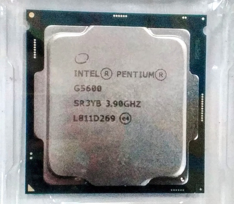
As far as their Single Core performance goes, they are as capable as the i7 and i9 CPUs. The only major difference between an i5 and i7/i9 is the core count.
In terms of multi core performance an i5 is weaker than an i7/i9 however, UNLESS you are a professional editor who renders tons of videos or if you a regular streamer who streams games while playing them on ultra high settings, an i5 should more than suffice.
Also Read: Does Motherboard Matter for Gaming?
Final Words
It is funny to even draw a comparison between Intel Pentium vs i5 since an i5 is literally a beast in front of Pentium.
However, for the uninitiated and new PC builders, things can get confusing particularly given the fact that Intel has so many different lines of CPUs and understanding each and their sub models can give even adepts a headache.
Also Read: Difference Between Intel Celeron vs i3
The Story of the abandoned Intel 7 GHz Pentium 5 chips
YouTube channel Fully Buffered published a video yesterday discussing the history of the abandoned Tejas Project by Intel.![]() This project would have seen two Pentium 5 chips hit the market offering significantly higher clock speeds on a single core — between 7-10 GHz depending on the chip. The project was shelved due to power consumption and overheating issues, and Intel changed the company’s focus to multi-core processors.
This project would have seen two Pentium 5 chips hit the market offering significantly higher clock speeds on a single core — between 7-10 GHz depending on the chip. The project was shelved due to power consumption and overheating issues, and Intel changed the company’s focus to multi-core processors.
First, let’s look a little closer into the two chips themselves. Tejas was the codename given to the microprocessor to be the successor to the Pentium 4 processor. Jayhawk was the Xeon variant of the abandoned Pentium 5 series.
Intel’s Core formed the basis for power-efficient architectures. Netburst, the microarchitecture for the x86 processors, was launched in November 2000. The microarchitecture was seen in the Willamette-core Pentium 4 series, the first release of the newer processors. Netburst was also utilized in Pentium D variations until July 2006, when the company chose to replace the microarchitecture with the more contemporary Core architecture.
In 2003, Intel began work on the Tejas series, with a release date the following year. However, due to issues with the designs of the chips, Intel was forced to change the date to 2005. Unfortunately, the company could not achieve its goal with the Tejas Project and ended the development on May 7, 2004. Outside of heat and high power consumption causing issues with the product, there was also the issue of sacrificing the processors’ performance per clock.
Image source: Jason R. Wilson, Wccftech. All assets are owned by their significant owners.
Issues similar to this were seen with the Prescott performance and its minor gain above Northwood. Prescott could obtain clock speeds over 5 GHz but suffered increased power and higher temperatures, albeit mildly. Intel’s Tejas was to achieve higher clock speeds than Prescott. The company attempted to achieve clock speeds reaching a fantastic 10 GHz within ten years (2000 to 2011). However, as the YouTuber points out, Prescott was a disaster.
The Tejas and Jayhawk chips were to enhance and improve NetBurst, with Tejas being built with a 90nm process. Eventually, the chip had to reduce from a 90 nm process to a 65 nm process. At the time, the series was to offer a single megabyte of L2 cache. The 65 nm processor doubled the cache size of the 90 nm chip, offering 2 MB of L2 cache. A rumored dual-core processor called Cedar Mill by Intel was also to be developed but never saw the light of day.
Regarding specifications of the Tejas processor, Various outlets reported that early samples sent to board partners showed that the clock reached 2.8 GHz with a TDP of 150W. The unreleased CPU would have fit into the LGA 775 socket with a die size of 213 mm² — double that of the Prescott chipset. The only sample reported before the video from Fully Buffered was from Anandtech, who obtained a model that turned out to be the Prescott BO ES and not the Tejas series. The only speculated samples that would have been floating around in enthusiast circles would have possibly thermal examples of the Tejas line.
Fully Buffered obtained the Tejas and Jayhawk processors from John Culver of CPU Shack (eBay) for an undisclosed amount. The YouTuber said the Tejas chip fit into an LGA 771 socket, not the reported LGA 775 socket. Intel labeled them with the name «j-holes.» The date listed on the chips and verified by the RoHS documentation is in the middle of April 2004, which is assumed only to be a few weeks before the company entirely scrapped the line.
Steve Fischer, one of the Intel engineers who worked on the Tejas and Jayhawk processors, gave some insight into some of the development histories and is not currently reported anywhere but on Fully Buffered’s channel.
The first question focused on Fischer’s involvement with the project and some insights into the project.
Tejas was primarily led and developed by an engineering team based in Austin, and the Folsom processor development team playing a large existing role. Folsom had more is and designed for manufacturability expertise based on earlier P6 and P4 derivative product developments, while the Austin team was newer to intel but with some different microarchitecture expertise brought in from the outside like former Power PC engineers.
I came into this project late having spent a couple of years doing something completely different at one of intel’s acquisitions during the .com boom […] after returning to intel I focused on microcode development. With these efforts are first being applied on Prescott and then later on Tejas the latest and greatest P4 product. The thing had a pipeline depth of around 50 stages and an expected clock target at one point north of 7 GHz.
I call the thing «the Death Star of processors» and half-jokingly reasoned that consumer acceptance of liquid-cooled chassis would not be a big deal.
By mid-2004, I believe I’d moved on to lead the microarchitecture activities [at Intel.]…
The fastest Pentium 4 processor at the time offered 3.8 GHz at 115W TDP, so the Tejas would have provided at the 7 GHz level around 250W TDP or higher, which at that time would have required liquid-cooling to keep heat levels low.
Fischer was then asked about the project within intel, especially when the microarchitecture was the gateway to the beginning of the Core architecture.
This «multiple team approach» is quite common at intel. It is healthier and encourages a more competitive product. Development at the time, as also on many other products, there was a lot of debate between which architecture direction was best. Even within the teams, there’s been a lot of debate. Tejas, in a way, was taking the P4 microarchitecture to an even further extreme while many believed that this was a dead end due to its extreme use of pipelining and the power implications that came with it while the more recent trend towards mobility and lower power implied the mirror on direction to be the better choice.
After Merom team was showing very favorable results, and given these doubts, it was decided at a corporate level to kill Tejas and double-down on the mirror microarchitecture.
Fully Buffered asked if Fischer could comment on the legitimacy of the two processors purchased from Culver off eBay, to which the former Intel engineer stated:
.
..2004 is the year in which the project was cancelled. After having some early silicon results, and I believe these are probably actual silicon. The A4 stepping designation makes that implication as it would be highly unlikely to have that many revisions for a thermal or mechanical sample.
On the origin of the names of the two processors, Fischer had this to say about their history:
I think it is named after a park or river in Texas. Not sure about Jayhawk…
One shouldn’t put too much weight on such project names as often it may be simply based on the whims of a more influential manager that also passes the approval of the legal department.
During the interview, Fischer was asked if he believed the processor would be capable of working, to which he stated that he was unsure but would lean strongly towards the processor not working. Fully Buffered attempted an older and newer Intel board and failed to activate the processor.
Halting an entire project is a multi-million dollar loss regarding a business’s expenses. With Intel, canceling Tejas and Jayhawk had quite a dramatic effect as their first attempt at a dual-core processor for the company’s Itanium processor that was marketed for enterprise servers and high-performance computing systems. Also, AMD was developing and releasing the company’s Athlon 64 processors, which were a giant step for the Intel rival.
The company immediately switched its focus to the Pentium M microarchitecture, which used some of the same building blocks as the P6 architecture used in their Centrino notebooks. The microarchitecture was a more considerable step for Intel in that it not only outperformed several NetBurst-based designs but, in turn, ushered in the Core processors, leading to the Core 2 architectures that are used to this day. But even to this day, the GHz race is more alive than ever with both AMD and Intel pushing their latest chips past the 5. 5 GHz barrier and closer to the 6.0 GHz clock limit.
News Sources: Fully Buffered, Anandtech
COMPANY NEWS; Flaw Undermines Accuracy of Pentium Chips
Business|COMPANY NEWS; Flaw Undermines Accuracy of Pentium Chips
Advertisement
Continue reading the main story
COMPANY NEWS
Credit…The New York Times Archives
See the article in its original context from
November 24, 1994, Section D, Page 1Buy Reprints
View on timesmachine
TimesMachine is an exclusive benefit for home delivery and digital subscribers.
About the Archive
This is a digitized version of an article from The Times’s print archive, before the start of online publication in 1996. To preserve these articles as they originally appeared, The Times does not alter, edit or update them.
Occasionally the digitization process introduces transcription errors or other problems; we are continuing to work to improve these archived versions.
An elusive circuitry error is causing a chip used in millions of computers to generate inaccurate results in certain rare cases, heightening anxiety among many scientists and engineers who rely on their machines for precise calculations.
The flaw, an error in division, has been found in the Pentium, the current top microprocessor of the Intel Corporation, the world’s largest chip maker. The chip, in several different configurations, is used in many computers sold for home and business use, including those made by I.B.M., Compaq, Dell, Gateway 2000 and others.
The flaw appears in all Pentium chips now on the market, in certain types of division problems involving more than five significant digits, a mathematical term that can include numbers before and after a decimal point.
Intel declined to say how many Pentium chips it made or sold, but Dataquest, a market research company in San Jose, Calif. , estimated that in 1994 Intel would sell 5.5 million to 6 million Pentiums, roughly 10 percent of the number of personal computers sold worldwide.
Intel said yesterday that it did not believe the chip needed to be recalled, asserting that the typical user would have but one chance in more than nine billion of encountering an inaccurate result as a consequence of the error, and thus there was no noticeable consequence to users of business or home computers. Indeed, the company said it was continuing to send computer makers Pentium chips built before the problem was detected.
William Kahan of the University of California at Berkeley, one of the nation’s experts on computer mathematics, expressed skepticism about Intel’s contentions that the error would only occur in extremely rare instances.
«These kinds of statistics have to cause some wonderment,» he said. «They are based on assertions about the probability of events whose probability we don’t know.»
At the Jet Propulsion Laboratory in Pasadena, Calif. , one satellite communications researcher who learned of the error this week, said six Pentium machines were used in his group and their use had been suspended for now.
«The Pentium appeared as a cost-effective means to do the kind of analytical computing that scientists and engineers do,» said David Bell, the researcher. «But when we hear and see that there are problems, that puts a question mark on the results.»
A number of other computer scientists and engineers said the probability of encountering the problem would vary wildly depending upon what software the computer was using.
In addition to its growing role in PC’s, the Pentium chip is used in a number of larger computers that harness individual chips to work in tandem, creating supercomputer power. This technique, known as parallel processing, is used for weather forecasting, the aerodynamic simulation used in automotive and airplane design and in molecular engineering.
Intel said the problem came to its attention in June and was corrected then, at the design stage. That change took some time to make its way through the chip production process, and Intel has only recently begun providing its largest customers with the revised chips, the company said.
Intel acknowledged that the flaw could affect certain scientific and engineering applications in rare cases. Stephen L. Smith, the company’s engineering manager for the Pentium, said discussions were under way with scientists and engineers.
«Those are exactly the people who should call us,» he said. «We’re willing to work with them and understand what applications they are using that might be affected.»
For Intel, which has spent millions of dollars on an advertising campaign using the slogan «Intel Inside,» the news of the defect might create something of a public relations problem. In recent months Intel has had success in positioning the Pentium as a chip for scientific and engineering applications, boasting that at a lower cost it matches the speed of rival processors made by Digital Equipment, Hewlett-Packard, I. B.M. and Sun Microsystems.
«The issue is being sure that the arithmetic is right,» said Cleve Moler, chairman and chief scientist of the Mathworks, a software company in Natick, Mass., that develops mathematical software. «There are enough other things that can go wrong that I don’t want to think about arithmetic.»
The Pentium flaw is not the first to be found in microprocessors. Both Intel’s 386 and 486 chips, predecessors of the Pentium that remain in wide use, have had different math errors that were corrected when they were discovered. And in 1991 Sun Microsystems acknowledged that a division error in its Sparc work stations created a security loophole. That problem was later corrected.
Some computer users said they believed that Intel had not acted quickly enough after discovering the error.
«Intel has known about this since the summer; why didn’t they tell anyone?» said Andrew Schulman, the author of a series of technical books on PC’s. «It’s a hot issue, and I don’t think they’ve handled this well.
The company said that after it discovered the problem this summer, it ran months of simulations of different applications, with the help of outside experts, to determine whether the problem was serious.
The Pentium error occurs in a portion of the chip known as the floating point unit, which is used for extremely precise computations. In rare cases, the error shows up in the result of a division operation.
Intel said the error occurred because of an omission in the translation of a formula into computer hardware. It was corrected by adding several dozen transistors to the chip.
The error was made public earlier this month after Thomas Nicely, a mathematics professor at Lynchburg College in Lynchburg, Va., sent a private electronic-mail message to several colleagues, asking them to check their machines for the error. Dr. Nicely was calculating a series of reciprocals of prime numbers, in part to show that PC’s now had enough power to be used instead of supercomputers for computationally intensive tasks.
Professor Nicely, who is now consulting with Intel, said he had run more than one quadrillion calculations on a revised Pentium chip and had not reproduced the error.
After the Pentium flaw was made public, Intel began telling users that it had discovered and corrected the flaw in June, and last week it quietly began offering replacement chips to users concerned about the error.
Executives at the Compaq Computer Corporation and the Dell Computer Corporation, two large Pentium customers, said they had begun to receive calls from users who had found the error using a test recommended by Professor Nicely.
A spokeswoman for Compaq said the company was referring the calls to Intel. A spokesman for Dell said the company had been contacted recently by Intel and was dealing directly with customers.
0029
15W vs 54W
Why is Intel Pentium G3430 better than Intel Core i5-4200U?
- 2.
 06x higher CPU speed?
2 x 3.3GHz vs 2 x 1.6GHz - GPU frequency 150MHz more?
350MHz vs 200MHz - 1 newer version of PCI Express (PCIe)?
3 vs 2 - 16GB more max memory?
32GB vs 16GB - Supports memory debug code?
- 100MHz faster GPU turbo speed?
1100MHz vs 1000MHz
Which comparison is the most popular?
Intel Core i5-4200u
VS
Intel Celeron N3060
Intel Pentium G3430
VS
AMD E1-1200
Intel Core i5-4200u
003
Intel Pentium G3430
vs
Intel Core i7-4930K
Intel Core i5-4200U
vs
Intel Core i3-7100
Intel Pentium G3430
vs
Intel Core i3-2100
Intel Core i5-4200U
VS
Intel Celeron N4020
Intel Pentium G3430
VS
AMD E1-2500
Intel Core Gore
VS
Intel Ceoleon N3000 INTEL INTEL INTEL INTEL INTEL INTEL INTEL INTEL INTEL INTEL0003
VS
Intel Core i5-3470
Intel Core i5-4200U
VS
A10-57503
Intel Pentium G3430
VS
Apple M1
Intel Core INTEL INTEL INTEL INTEL INTEL Intel Core i5-1135G7
Intel Pentium G3430
VS
Intel Core i5-2400
Intel Core i5-4200U
AMD AMD AMD AMD AMD AMD AMD G34303
Intel PENTIUM
Intel Core i5-4200u
VS
AMD A6-5350M
Intel Pentium G3430
VS
Intel Celeron G5905
9002
Users 9000-based productivity Production Production Production Productivity Production Protection.
 x 1.6GHz
2 x 3.3GHz
CPU speed indicates how many processing cycles per second a processor can perform, considering all its cores (processors). It is calculated by adding the clock speeds of each core or, in the case of multi-core processors, each group of cores.
2nd processor thread
More threads result in better performance and better multitasking.
3.speed turbo clock
2.6GHz
Unknown. Help us offer a price. (Intel Pentium G3430)
When the processor is running below its limits, it can jump to a higher clock speed to increase performance.
4. Has an unlocked multiplier of
✖Intel Core i5-4200U
✖Intel Pentium G3430
Some processors come with an unlocked multiplier and are easier to overclock, allowing you to get better performance in games and other applications.
5. L2 Cache
More L2 scratchpad memory results in faster results in CPU and system performance tuning.
6.L3 cache
More L3 scratchpad memory results in faster results in CPU and system performance tuning.
7.L1 cache
More L1 cache results in faster results in CPU and system performance tuning.
8.core L2
0.25MB/core
0.25MB/core
More data can be stored in the L2 scratchpad for access by each processor core.
9.core L3
1.5MB/core
1.5MB/core
More data can be stored in L3 scratchpad memory to access each processor core.
Memory
1.RAM speed
1600MHz
1600MHz
Can support faster memory which speeds up system performance.
2.max memory bandwidth
25. 6GB/s
6GB/s
25.6GB/s
This is the maximum rate at which data can be read from or stored in memory.
3rd DDR memory version
Unknown. Help us offer a price. (Intel Pentium G3430)
DDR (Double Data Rate Synchronous Dynamic Random Access Memory) is the most common type of RAM. New versions of DDR memory support higher maximum speeds and are more energy efficient.
4 memory channels
More memory channels increase the speed of data transfer between memory and processor.
5.maximum memory capacity
Maximum memory capacity (RAM).
6.bus baud rate
Unknown. Help us offer a price. (Intel Core i5-4200U)
Unknown. Help us offer a price. (Intel Pentium G3430)
The bus is responsible for transferring data between various components of a computer or device.
7. Supports Memory Error Code
✖Intel Core i5-4200U
✔Intel Pentium G3430
Memory Error Code can detect and repair data corruption. It is used when necessary to avoid distortion, such as in scientific computing or when starting a server.
8.eMMC version
Unknown. Help us offer a price. (Intel Core i5-4200U)
Unknown. Help us offer a price. (Intel Pentium G3430)
A newer version of eMMC — built-in flash memory card — speeds up the memory interface, has a positive effect on device performance, for example, when transferring files from a computer to internal memory via USB.
9.bus frequency
Unknown. Help us offer a price. (Intel Core i5-4200U)
Unknown. Help us offer a price. (Intel Pentium G3430)
The bus is responsible for transferring data between various components of a computer or device
Geotagging
1. PassMark result
Unknown. Help us offer a price. (Intel Pentium G3430)
This benchmark measures processor performance using multithreading.
2nd PassMark result (single)
Unknown. Help us offer a price. (Intel Pentium G3430)
This test measures processor performance using a thread of execution.
3.Geekbench 5 result (multi-core)
Unknown. Help us offer a price. (Intel Pentium G3430)
Geekbench 5 is a cross-platform benchmark that measures multi-core processor performance. (Source: Primate Labs,2022)
4. Cinebench R20 result (multi-core)
Unknown. Help us offer a price. (Intel Pentium G3430)
Cinebench R20 is a test that measures the performance of a multi-core processor by rendering a 3D scene.
5.Cinebench R20 result (single core)
Unknown. Help us offer a price. (Intel Pentium G3430)
Cinebench R20 is a test to evaluate the performance of a single core processor when rendering a 3D scene.
6.Geekbench 5 result (single core)
Unknown. Help us offer a price. (Intel Pentium G3430)
Geekbench 5 is a cross-platform benchmark that measures the single-core performance of a processor. (Source: Primate Labs, 2022)
7. Blender test result (bmw27)
Unknown. Help us offer a price. (Intel Core i5-4200U)
Unknown. Help us offer a price. (Intel Pentium G3430)
The Blender benchmark (bmw27) measures CPU performance by rendering a 3D scene. More powerful processors can render a scene in a shorter time.
8.Blender result (classroom)
Unknown. Help us offer a price. (Intel Core i5-4200U)
Unknown. Help us offer a price. (Intel Pentium G3430)
The Blender (classroom) test measures CPU performance by rendering a 3D scene. More powerful processors can render a scene in a shorter time.
9.performance per watt
Unknown. Help us offer a price. (Intel Core i5-4200U)
Unknown. Help us offer a price. (Intel Pentium G3430)
This means that the processor is more efficient, giving more performance per watt of power used.
Functions
1.uses multithreading
✔Intel Core i5-4200U
✔Intel Pentium G3430
processor into logical cores, also known as threads. Thus, each core can run two instruction streams at the same time.
2. Has AES
✔Intel Core i5-4200U
✖Intel Pentium G3430
AES is used to speed up encryption and decryption.
3. Has AVX
✔Intel Core i5-4200U
✔Intel Pentium G3430
AVX is used to help speed up calculations in multimedia, scientific and financial applications, and to improve the performance of the Linux RAID program.
4.Version SSE
SSE is used to speed up multimedia tasks such as editing images or adjusting audio volume. Each new version contains new instructions and improvements.
5.Has F16C
✔Intel Core i5-4200U
✔Intel Pentium G3430
F16C is used to speed up tasks such as image contrast adjustment or volume control.
6.bits transmitted at the same time
Unknown. Help us offer a price. (Intel Core i5-4200U)
Unknown. Help us offer a price. (Intel Pentium G3430)
NEON provides faster media processing such as MP3 listening.
7. Has MMX
✔Intel Core i5-4200U
✔Intel Pentium G3430
MMX is used to speed up tasks such as adjusting image contrast or adjusting volume.
8. Has TrustZone
✖Intel Core i5-4200U
✖Intel Pentium G3430
Technology is integrated into the processor to ensure device security when using features such as mobile payments and video streaming through Digital Rights Management (DRM) technology .
9.interface width
Unknown. Help us offer a price. (Intel Core i5-4200U)
Unknown. Help us offer a price. (Intel Pentium G3430)
The processor can decode more instructions per clock (IPC), which means the processor performs better
Price comparison
Cancel
Which CPUs are better?
Pentium birthday. The famous processor is 29 years old / Sudo Null IT News On this day, a solemn presentation took place, at which Intel presented to the public a new generation of processors called Pentium — chips that radically changed the familiar landscape of computer technology in the first half of the «nineties».
Microprocessor engineer and venture capitalist Vinod Dham, known as the «Father of the Pentium,» began working on the next-generation x86-compatible processor architecture, tentatively called the P5, back in 1989. The first prototypes appeared in 1991, after which a long process of testing a new microcircuit, eliminating shortcomings, optimizing its topology and preparing for mass production began. Initially, it was assumed that these chips would be called 80586 or i586 by analogy with the previous generation Intel processors — 386 and 486, but here the manufacturer encountered an unexpected problem. The fact is that competing companies quickly launched the production of cheaper analogues of Intel processors, which were successfully sold under similar names, such as, for example, Am486 from AMD or 486SLC/486DLC from Cyrix Corporation. To protect its products from such «piracy», Intel tried to patent the name «586», but it quickly became clear that the trademark under US law could not consist of numbers alone. That is why it was decided to name the fifth generation processors Intel Pentium — from the Greek word «pente», «five».
The official presentation of the Intel Pentium took place on March 22, 1993 — this day is considered to be the birthday of the Pentiums. Serial production of Pentium processors with a core clock speed of 60 MHz had already been established at the Intel factory in Oregon by that time. Of course, the new chip significantly surpassed the 486-series processors that reigned on the market at that time both in terms of performance and speed, thanks to which it quickly gained popularity.
The new processor was based on 800 nm technology and included 3.1 million transistors per chip. Due to the presence in its architecture of two pipelines — the main and auxiliary — Intel Pentium could execute two commands in one cycle, which significantly increased its performance. In fact, the Pentium became the first x86 processor with a multi-pipeline architecture. Thanks to the use of a 64-bit data bus, it could exchange twice as much information with memory in one cycle as compared to previous generation processors at a similar clock speed. The Intel Pentium used a 16 KB L1 cache, but at the same time it was split into 2 segments of 8 KB each for separate storage of data and instructions, which again gave a performance gain compared to 80486. The Pentium also had other important differences from its predecessors, for example , a branch prediction (branch prediction) mechanism that made it possible to use the idle time of pipelines to preload and execute instructions that should be executed after a conditional branch instruction. The Pentium’s prediction accuracy was quite high, which made it possible to further optimize the computing resources of the processor. In addition, the «Pentium» supported the system management mode (System Management Mode, SMM), which opened up the possibility of reducing its power consumption.
The first Pentium 60 model based on the P5 core was produced in a 273-pin Socket 4 package. At the same time, serial production of Intel Pentium for notebooks began, which rapidly gained popularity due to high performance, especially in games. In the same 1993, Intel launched the production of a modification with a frequency of 66 MHz, but this processor heated up much more than the first model and already required the installation of a fan (Intel Pentium 60 perfectly managed with a conventional passive cooling radiator). In addition, the percentage of defects in the manufacture of these chips was too high, which is why they were quickly removed from production, replacing them with a new version of the processor, released on the basis of 600-nanometer technology with an updated P54C core. This version was capable of operating at a frequency of 75 MHz.
It was this processor that became one of the most massive and popular in this family. In addition, it quickly became clear that Pentium processors are capable of operating in forced modes, which is why numerous instructions and methods for their “overclocking” appeared, which were successfully used, first of all, by gamers.
In 1994, Pentium processors based on the P54C core with frequencies of 90 and 100 MHz were born, and in the latter it was possible to reduce the supply voltage to 3.3 V, and the power consumption to 10.1 W. These processors were installed in a different socket — Socket 5, and their main distinguishing feature was that the clock frequency of the processor core exceeded the frequency of the system bus.
In 1995, Intel launched the little-known Pentium OverDrive series processors. They had all the features and capabilities of the first generation Pentium processors on the P5 core, but were intended for installation in Socket 2 and Socket 3, which made it possible to upgrade computers with i486 processors without replacing the motherboard. This processor worked with a voltage of 5 V, two modifications were released with frequencies of 63 and 83 MHz. However, Pentium OverDrive did not gain popularity due to the combination of high cost and low performance: in most cases, users were more profitable to invest in replacing the processor + motherboard kit, getting a computer with a higher clock speed and faster performance, which, moreover, could be upgraded in the future, a simple replacement of the processor.
Soon a modification of the Pentium core was developed under the name P54CS — these processors were produced using a 350-nanometer process technology, which made it possible to further reduce the size of the crystal. In 1995 and 1996, chips with a frequency of 120, 133, 150 and 166 MHz were born in this family.
The next milestone in Pentium history was the introduction of MMX technology and the new P55C core. Developed at the Israeli research center in Haifa, the MMX instruction set significantly improved processor performance in multimedia applications and games, and the increase could reach 60% if the new instructions were fully supported by the program itself. The first-level cache of the new Pentium MMX family was increased to 32 KB (16 for data and instructions each), and the chip itself, produced using 280-nanometer technology, included 4.5 million transistors.
In January 1997, an extremely popular hit called the Intel Pentium 166 MMX was born, which broke almost all records in terms of the number of copies sold, a little later the Pentium 200 MMX joined it. The last serial processor in this family was the Intel Pentium 233 MMX, which went on sale on June 2, 1997. This chip ended the long history of Pentium processors, which began 29 years ago.
Surprisingly, some computers and laptops with Pentium processors work fine to this day, which indicates their high reliability. Of course, the Pentium II, III and IV that followed them were much more advanced, but the first generation of Intel Pentium was a real breakthrough that forever changed the world of high technology.
Evolution of the Pentium
This entry is entered into our paper competition.
In just over 10 years of existence, Intel’s Pentium processors have come a long way. Only the clock frequency has increased by more than 53 times, from 60 MHz to 3200 MHz. Also, Intel is the author of many developments that were later used by companies such as AMD and VIA.
The following processor families have been released in these 10 years:
- 1993 — Intel Pentium
- 1995 — Intel Pentium PRO
- 1997 — Intel Pentium MMX
- 1997 — Intel Pentium II
- 1999 — Intel Pentium!!!
- 2000 — Intel Pentium 4
And now let’s look at each of them in more detail.
Pentium
It all started on March 22, 1993. It was then that Intel introduced the first processors under the brand name Pentium , which for many years became synonymous with the word processor.
recommendations
This was the first dual-pipeline processor. Had the code name P5 . Had clock frequencies of 60 and 66 MHz. The bus frequency coincided with the processor clock speed. The processors contained more than 3.1 million transistors and were produced using 0.80 micron technology, and later — 0.60 micron. The size of the first level L1 cache was 16 KB — 8 KB for data and 8 KB for instructions, while the second level cache was located on the motherboard and could be up to 1 MB. The processor was produced for Socket 4.
A year later, in March 1994, Intel releases the second generation Pentium (core P54 ).
The processor had frequencies from 75 to 200 MHz. Bus frequency 50-66 MHz. The size of the L1 cache remained the same — 16 KB (8 KB for data and 8 KB for instructions). The second-level cache remained on the motherboard, and could have a volume of up to 1 MB. In the manufacture of this processor, Intel uses a more advanced 0.50 micron process technology. The processor contained over 3.3 million transistors. Released for Socket 5, later Socket 7.
Pentium PRO
On November 1, 1995, with the release of the Pentium PRO processor (codename P6 ), the sixth generation of processors began to count down. They were distinguished from the previous generation by the use of dynamic execution technology — changing the order of execution of instructions and the architecture of a double independent bus. Another bus has been added that connects the processor to the second-level cache, which is built into the core. As a result, for the first time, an L2 cache operating at the processor frequency was used. The initial size of the L2 cache is 256 KB; by 18 August 1997 reached 1024 KB. The maximum size is 2048 Kb. The cache of the first level remained the same: 8 KB + 8 KB. Had clock frequencies of 150, 166, 180, 200 MHz.
Pentium PRO processors were produced in SPGA (Staggered Pin Grid Array) packages with pin matrix. Two crystals were installed in one case — the processor core and the second-level cache of our own manufacture.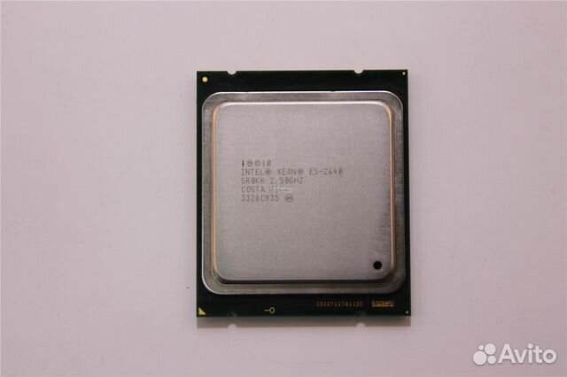 Installed in Socket 8 with the ability to combine up to 4 processors for symmetrical multiprocessing. Bus 60-66 MHz. With 32-bit computing and multitasking, it significantly outperformed the Pentium, but lost to it in 16-bit applications. The 150 MHz processor was manufactured using a 0.60 micron process technology, older models — 0.35 micron. Pentium PRO consisted of more than 5.5 million transistors, plus from 15.5 to 31 million included a cache. Pentium MMX
On January 8, 1997, the Pentium w/MMX technology processor (codename P55 ) was released, which is a continuation of the Pentium line, in which a new set of 57 MMX (Multi Media eXtention) instructions was first implemented, significantly increasing computer performance in multimedia applications (from 10 to 60%, depending on optimization).
Available in 166, 200 and 233 MHz. Worked on 66 MHz bus. Compared to the Pentium, the size of the first level cache was doubled, which amounted to 32 KB. As in previous versions, a separate cache was used: 16 KB for data and 16 KB for instructions. It is worth saying that such a division (and size) of the L1 cache has become a kind of standard for many years. The second-level cache, like its predecessor, remained on the motherboard, and could have a volume of up to 1 MB. The processors were produced according to 0.35 micron technology, and consisted of 4.5 million transistors. Designed for Socket 7.
Pentium II
The first processors with the name Pentium II appeared on May 7, 1997. These processors combine the Pentium PRO architecture and MMX technology. Compared to Pentium Pro, the size of the primary cache has been doubled (16 KB + 16 KB). The processor uses a new package technology — a cartridge with a printed edge connector, on which the system bus is displayed: S.E.C.C (Single Edge Contact Cartridge). It was produced in the Slot 1 design, which naturally required an upgrade of old motherboards. A 14 x 6.2 x 1. 6 cm cartridge has a processor core chip (CPU Core), several chips that implement the secondary cache, and auxiliary discrete elements (resistors and capacitors).
This approach can be considered a step backwards — Intel has already worked out the technology of embedding the second-level cache into the core. But in this way it was possible to use third-party memory chips. At one time, Intel considered this approach promising for the next 10 years, although after a short time it is abandoned.
At the same time, the independence of the secondary cache bus is preserved, which is closely connected to the processor core by its own local bus. The frequency of this bus was half that of the core. So the Pentium II had a large cache running at half the processor speed.
The first Pentium II processors (codename Klamath ), which appeared on May 7, 1997, had about 7.5 million transistors in the processor core alone and were made using 0. 35 micron technology. They had core clocks of 233, 266 and 300 MHz with a system bus frequency of 66 MHz. At the same time, the secondary cache worked at half the core frequency and had a volume of 512 KB. For these processors, Slot 1 was developed, which in terms of signal composition strongly resembles Socket 8 for the Pentium Pro. However, Slot 1 allows only a couple of processors to be combined to implement a symmetrical multiprocessor system, or a system with redundant functionality control (FRC). So this processor is a faster Pentium Pro with MMX support, but with reduced multiprocessor support.
On January 26, 1998, a processor from the Pentium II line came out with the name of the core — Deschutes . Klamath differed from in a thinner technological process — 0.25 µm and a bus frequency of 100 MHz. Had clock frequencies of 350, 400, 450 MHz. It was produced in the S.E.C.C design, which in older models was changed to S.E.C.C.2 — a cache on one side of the core, and not on two, as in the standard Deschutes, and a modified cooler mount. The last core officially used in Pentium II processors, although the latest Pentium II 350-450 models came with a core that looked more like Katmai — only, of course, with a cut SSE. Remained support for MMX. The cache of the first level is the same 32 KB (16 + 16). The second level cache has not changed either — 512 KB running at half the frequency. The processor consisted of 7.5 million transistors and was produced for the Slot 1 connector.
Pentium II OverDrive — this was the name of the processor released on August 11, 1998 to upgrade the Pentium PRO on old motherboards, and working in the Socket 8 socket).
Had the code name P6T . Had a frequency of 333 MHz. The first level cache is 16 KB for data + 16 KB for instructions, the second level cache had a size of 512 KB and was integrated into the kernel. Worked at the frequency of the processor. Bus 66 MHz. It contained 7.5 million transistors and was produced according to the 0.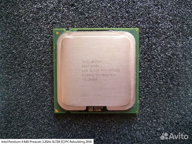 25 micron process technology. Supported the MMX instruction set.
Celeron
A new branch in the direction of microprocessor technology for Intel was the release of parallel mainstream, «lightweight» and cheaper versions. This is the Celeron series. On April 15, 1998, the first processor was introduced, called the Celeron and operating at a clock frequency of 266 MHz.
Codename Covington . This processor is a cut-off Pentium II. Celeron is based on kernel Deschutes without L2 cache. Which, of course, affected its performance. But it accelerated just fine (from one and a half to two times). If Pentium II overclocking was limited by the maximum cache frequency, then it simply did not exist here!
Celeron worked on a 66 MHz bus and repeated all the main characteristics of its ancestor — Pentium II Deschutes: L1 cache — 16 KB + 16 KB, MMX, 0.25 micron process technology. 7.5 million transistors. The processor was produced without a protective cartridge — constructive — S.E.P.P (Single Edge Pin Package). Connector — Slot 1.
Starting with a frequency of 300 MHz, Celeron processors appeared with a 128 KB cache integrated into the core, operating at the processor frequency. Codename — Mendocino . It was released on August 8, 1998. Due to the full-speed cache, it has high performance comparable to Pentium II (assuming the same system bus frequency). They were produced with clock frequencies from 300 to 533 MHz. On November 30, 1998, a version of the processor with the P.P.G.A (Plastic Pin Grid Array) design was released, which worked in the Socket 370.
Up to 433 MHz available in two designs: S.E.P.P and P.P.G.A. For some time, Slot-1 (266 — 433 MHz) and Socket-370 (300A — 533 MHz) variants existed in parallel, in the end, the former was smoothly superseded by the latter.
The new Celeron was a step towards the Pentium !!!, but since it worked on a 66 MHz bus, it could not show all the advantages of the integrated high-speed cache. Since the cache was integrated into the core, the number of transistors that make up the processor has increased significantly — 19million. The process technology remained the same — 0.25 microns.
XEON
The Xeon family is designed for powerful computers. The Pentium II Xeon is a server variant of the Pentium II processor that replaced the Pentium PRO. It was produced on the Deschutes core and differed from the Pentium II in a faster (full-speed) and more capacious (there are options with 1 or 2 MB) L2 cache and design. It was produced in the S.E.C.C design for Slot 2. This is also an edge connector, but with 330 pins, a VRM voltage regulator, and an EEPROM storage device. Able to work in multiprocessor configurations. Was released on 29June 1998.
L2 cache, as in Pentium PRO, full speed. Only here it is on the same board with the processor, and is not integrated into the core. First level cache — 16 KB + 16 KB. Bus frequency — 100 MHz. Supported the MMX instruction set. The processor worked at frequencies of 400 and 450 MHz. Produced using the 0.25 micron process technology. and contained 7.5 million transistors.
This is where the development of the Pentium II line ends. Starting with the Pentium II, Intel has identified three main directions in the production of processors: Pentium is a high-performance processor for workstations and home use, Celeron is a budget version of a Pentium for office or home use, Xeon is a server version with increased performance.
Pentium!!!
The first processors with the name Pentium !!! not much different from the Pentium II. They worked on the same bus with a frequency of 100 MHz (later, from September 27, 1999, models operating on a 133 MHz bus appeared), were produced in the S.E.C.C. 2 and were designed for installation in Slot 1.
Cache memory remains the same: L1 — 16 KB + 16 KB. L2 — 512 Kb, located on the processor board, and operating at half the frequency of the processor.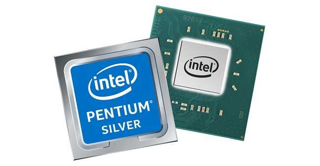 The main difference is the SIMD instruction set extension — SSE (Streaming SIMD Extensions). The set of MMX commands has also been expanded and the mechanism for streaming memory access has been improved. Kernel codename Katmai . Released February 26, 1999. The processor worked at frequencies of 450-600 MHz, contained 9.5 million transistors. Just like its predecessor — Pentium II Deschutes, it was produced using the 0.25 micron process technology.
Coppermine — this was the name of the next Pentium processor core !!!, which replaced Katmai on October 25, 1999. In fact, it is Coppermine that is a new processor, and not a revision of Deschutes. The new processor had a full-speed L2 cache integrated into the core with a size of 256 KB (Advanced Transfer Cache).
Manufactured using the 0.18 µm process. The thinning of the technology from 0.25 to 0.18 microns made it possible to place a larger number of transistors on the core and now there are 28 million of them, against 9. 5 million in old Katmai. True, the bulk of the newly introduced transistors refers to the integrated L2 cache. L1 cache remained unchanged. Supported MMX and SSE instruction sets. First produced in S.E.C.C. 2, but since the cache is now built into the processor core, the processor board was unnecessary, and only increased the cost of the processor. Therefore, soon the processors began to come out in the FC-PGA (Flip-Chip PGA) design. Like Celeron Mendocino, they worked in Socket 370.
True, there was limited compatibility with older motherboards. Since the processor was now running at higher clock speeds, the core was located on top, and had direct contact with the heatsink. Coppermine was the last processor for Slot 1. It worked on the 100 and 133 MHz bus (in the name of the processor, the 133rd bus was denoted by the letter B , for example — Pentium !!! 750B). Processors with the Coppermine core ran at clock speeds from 533 to 1200 MHz. The first attempts to release a processor based on this core with a frequency of 1113 MHz ended in failure, as it worked very unstable in extreme modes, and all processors with this frequency were recalled — this incident greatly tarnished Intel’s reputation.
Core Tualatin replaced Coppermine on June 21, 2001. At this time, the first Pentium 4 processors were already on the market, and the new processor was intended to test the new 0.13 micron. technology, as well as to fill the niche of high-performance processors, since the performance of the first Pentium 4 was rather low. Tualatin is the original name of Intel’s global project to move processor manufacturing to 0.13 micron technology. The processors themselves with the new core were the first products to appear as part of this project.
There are few changes in the core itself — only the «Data Prefetch Logic» technology has been added. It improves performance by preloading the data the application needs into the cache. In addition, the difference between these cores lies in the production technology used — Coppermine is manufactured using 0.18 micron technology, and Tualatin — 0.13 micron. The socket for the new processor remained the same — Socket 370, but the design changed to FC-PGA 2, which was used in Pentium 4 processors. It differs from the old FC-PGA in the first place in that the core is covered with a heat-dissipating plate, which also protects it from damage during installation of the radiator.
With the release of Tualatin, the Pentium line!!! «split» into two classes — desktop and server processors. For the former, the volume of the L2 cache remained at 256 KB, for the latter it doubled to 512 KB; also the desktop version of the new P-III (called Desktop Tualatin) lacked SMP support. First level cache — 16 KB + 16 KB. It should be said that Desktop Tualatin did not last long: it was supplied only to large PC assemblers, and was withdrawn from the market in order not to compete with Pentium 4. But Pentium !!!-S, the server version of the processor, was supposed to occupy the niche of powerful server processors, since the performance of Xeon processors was no longer enough, and the Pentium 4 did not have SMP support, and generally showed rather low performance.
As mentioned above, Tualatin processors were produced using a more advanced 0.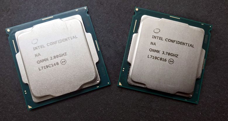 13 micron. process technology, worked on a bus with a frequency of 133 MHz and consisted of 44 million transistors. Supported MMX and SSE instruction sets. The processor ran at frequencies from 1 GHz to 1.33 GHz (Desktop Tualatin), and from 1.13 GHz to 1.4 GHz (server version).
Quite recently I found out quite interesting information — it turns out that Intel was developing a processor that was supposed to be a continuation of the Pentium line !!!. This processor was based on an upgraded Tualatin core using 0.13 µm. technical process. Its main differences from the usual Tualatin was increased to 1024 KB. L2 cache and 166 MHz system bus! Frequencies had to reach at least 2.0 GHz. But Intel, relying on the Pentium 4 processor, refuses the new Tualatin. After all, even if Celeron Tualatin, being overclocked to frequencies of about 1.7 GHz, easily competes not only with Celeron Willamette, but also with Pentium 4, then the new Tualatin, equipped with a huge cache and a fast bus, would not leave them any chance.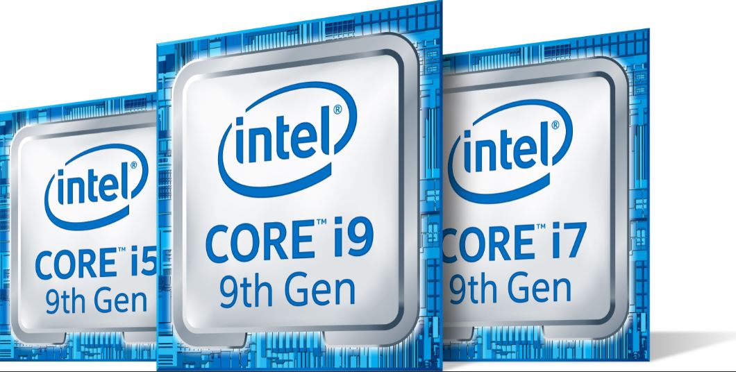
Celeron
After the release of the Pentium !!! processors, Intel, in order not to lose its positions in the market of budget processors, continued to release the Celeron line. Now they were completely different processors — Intel repeats the experience of creating the first processors with the name Celeron: it uses the Pentium processor core !!! with L2 cache trimmed to 128 KB and a slow 66 MHz bus.
March 29, 2000 the first Celeron processors appear on the Coppermine 128 9 core0518 or Coppermine Lite .
As the name implies, the processor is based on the Coppermine core with a halved L2 cache. Like the older brother — Pentium !!! Coppermine, the new Celeron, has a set of additional SSE commands, a fast built-in cache memory and is produced according to the same technological standard (0.18 microns.), differing only in the size of the second level cache — 128 KB versus 256 KB for Pentium !!! (the most annoying thing is that the cache is physically present in the processor, it is simply disabled).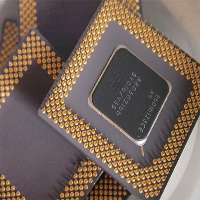 Works in the same Socket 370.
The first processors appeared with a frequency of 566 MHz and worked on a 66 MHz bus. Later, on January 3, 2001, with the release of the 800 MHz version, Celeron switched to a faster 100 MHz bus. The maximum frequency of these processors was 1100 MHz. First level cache: 32 KB (16 KB for data and 16 KB for instructions). The processor consisted of 28.1 million transistors.
On October 2, 2001, Intel moves the Celeron processor to a new core — Tualatin .
Celeron has never been so close to the Pentium processor. From Pentium!!! Desktop Tualatin, it differed only in a slower 100 MHz bus. In general, leaving the size of the L2 cache unchanged and lowering the FSB frequency to 100 MHz for the Tualatin core for desktop applications, Intel released the «new Celeron». The processors were produced with clock frequencies from 900 MHz to 1400 MHz, consisted of 44 million transistors, supported MMX, SSE. The technical process is 0.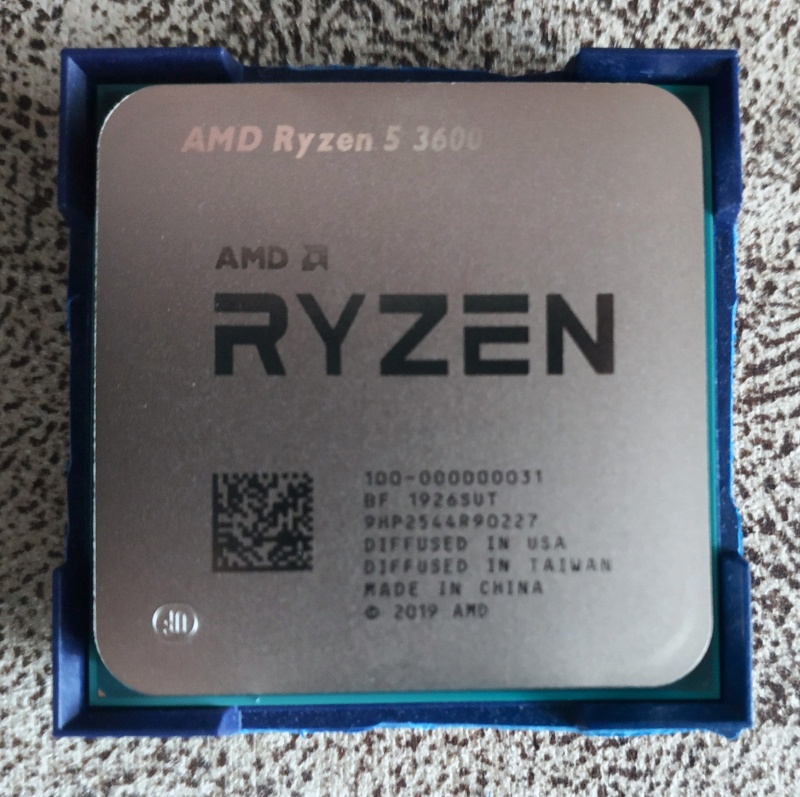 13 microns. Produced in FC-PGA 2 design, for Socket 370.
XEON
With the release of Pentium !!! Intel continues to release server processors based on the new generation Pentium. On March 17, 1999, the first processor from the Pentium line was released !!! xeon.
Core codename Tanner . It was built on the basis of Pentium!!! Katmai. Contains 512, 1024 or 2048 KB full-speed L2 cache. First level cache — 16 KB + 16 KB. Produced with frequencies of 500 and 550 MHz using 0.25 microns. technical process, and consisted of 9.5 million transistors. Worked on 100 MHz system bus. It was produced in the S.E.C.C design for Slot 2. It was intended for use in two-, four-, eight-processor (or more) servers and workstations.
With the transition Pentium !!! on October 25, 1999, a modification of the Xeon processor with a new core Cascades appeared on the new core. In fact, it was an upgraded Coppermine core. The processor had from 256 KB to 2048 KB cache of the second level, worked at the system bus frequencies of 100 and 133 MHz (depending on the version).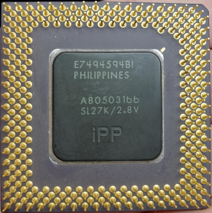 Processors were produced with frequencies from 600 to 900 MHz. Processors with a frequency of 900 MHz from the first batches overheated and their shipments were temporarily suspended. Like its predecessor, Xeon Cascades was designed for installation in the Slot 2 slot. It was produced using 0.18 microns. process technology and consisted of 28.1 million transistors. Could work in two-, four- and eight-processor servers and workstations.
No Xeon processors based on the Tualatin core. Their place was taken by the Pentium !!!-S, which I mentioned above. The Xeon processors supported the MMX and SSE instruction sets.
Pentium 4
Facing many problems when trying to increase the frequency of the Pentium processor !!! on the Coppermine core above 1 GHz, Intel engineers realized that the old processor architecture, which had not changed since the days of the Pentium Pro, required radical changes. And although the transition of production to 0.13 microns will help Pentium !!! for about a year it is quite worthy to do its job, the potential of this architecture is almost exhausted and the company has developed a new architecture for its new 32-bit processors, which it called Intel NetBurst Micro-Architecture. In order for processors to operate at frequencies of the order of several gigahertz, Intel increases the length of the Pentium 4 pipeline to 20 stages (Hyper Pipelined Technology), due to which it was possible to achieve processor operation at a frequency of 2 GHz even with technological standards of 0.18 microns. However, due to such an increase in the length of the pipeline, the execution time of one instruction in processor cycles also greatly increases. Therefore, the company has worked hard on transition prediction algorithms (Advanced Dynamic Execution).
The L1 cache in the processor has undergone significant changes. Unlike the Pentium !!!, whose cache could store instructions and data, the Pentium 4 has only 8 KB of data cache. Commands are stored in the so-called Trace Cache. There they are stored already in decoded form, i.e. in the form of a sequence of micro-operations coming for execution to the executive devices of the processor. The capacity of this cache is 12,000 µops.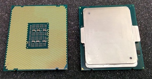
The instruction set has also been expanded in the new processor — SSE2 . In addition to 70 SSE instructions, 144 new instructions have been added. One of the many innovations was a completely new 100 MHz bus that transmits 4 data packets per clock — QPB ( Q uad P umped B us), which gives a resulting frequency of 400 MHz.
The first of the Pentium 4 line was the Willamette 423 processor.
Introduced on November 20, 2000 with frequencies of 1.4 and 1.5 GHz, these processors, manufactured using the 0.18 micron process technology, reached 2 GHz. The processor was installed in a new Socket 423 socket and produced in the FC-PGA 2 design. It consisted of 42 million transistors.
Level 2 cache remains the same size — 256 KB. The L2 cache bus is 256 bits wide, but the cache latency has been halved, allowing for a cache bandwidth of 48 GB at 1.5 GHz.
Since the architecture of the new processor was focused primarily on increasing the frequency, it is not surprising that the first Pentium 4 processors show extremely low performance. In most tasks, the 1.4 GHz processor was inferior to the Pentium !!! Coppermine operating at 1000 MHz.
Later, on August 27, 2001, processors with the Willamette core appeared designed for installation in a new socket — Socket 478. The processor repeated all the characteristics of its ancestor, except for the design — mPGA and socket 478.
The previous Socket 423 form factor was «transitional» and Intel is not going to support it in the future. The size of the processor has decreased due to the fact that now the conclusions are made directly under the processor core. This processor, like its predecessor, operated at frequencies from 1.4 to 2.0 GHz.
Northwood — this is the name of the next core, on which Pentium 4 processors are still produced to this day.
Transition to 0.13 µm. The technical process made it possible to further increase the clock frequency, and increase the second-level cache to 512 KB. The number of transistors that make up the processor has also increased — now there are 55 million of them. Naturally, support for the MMX, SSE and SSE2 instruction sets has remained.
The first processors based on the Northwood core appeared on August 7, 2001 with a frequency of 2.0 GHz and a system bus frequency of 400 MHz (4 * 100 MHz). Today, Northwood processors operate at frequencies from 1.6 to 3.2 GHz. To avoid confusion with processors operating at the same frequencies, but with a different core, Intel again uses letter marking. For example, Pentium 1.8 A , where the letter A indicates a new core and larger second level cache.
On May 6, 2002, Intel releases a processor based on the Northwood core with a system bus frequency of 533 MHz (4 * 133 MHz) and a clock frequency of 2.26 GHz. Since models with a bus frequency of 400 MHz were produced with frequencies up to 2.6 GHz, letter marking was also used here. Just like in Pentium processors!!! the presence of a 133 MHz bus was indicated by the letter B . For example, Pentium 4 2.4 B .
But Intel does not stop there, and on April 14, 2003 releases a processor based on the same Northwood core, but with a system bus frequency of 800 MHz (4 * 200 MHz) and a clock frequency of 3.0 GHz. Later, processors with an 800 MHz system bus began to be produced with lower frequencies — from 2.4 GHz. To indicate a new bus, the letter C appears in the processor marking. For example, Pentium 4 2.4 C . (Thus, there are three modifications of the 2.4 GHz processor with different bus frequencies that differ by a factor of 2!)
All 800MHz FSB processors support the new HT technology, which stands for Hyper-Threading .
Pentium 4 HT
On November 14, 2002, the Pentium 4 processor with a frequency of 3.06 GHz and a system bus frequency of 533 MHz was released with support for the new Hyper-Threading technology.
One physical processor with Hyper-Threading is seen by the system as two, which allows you to optimize the load of its resources and improve performance.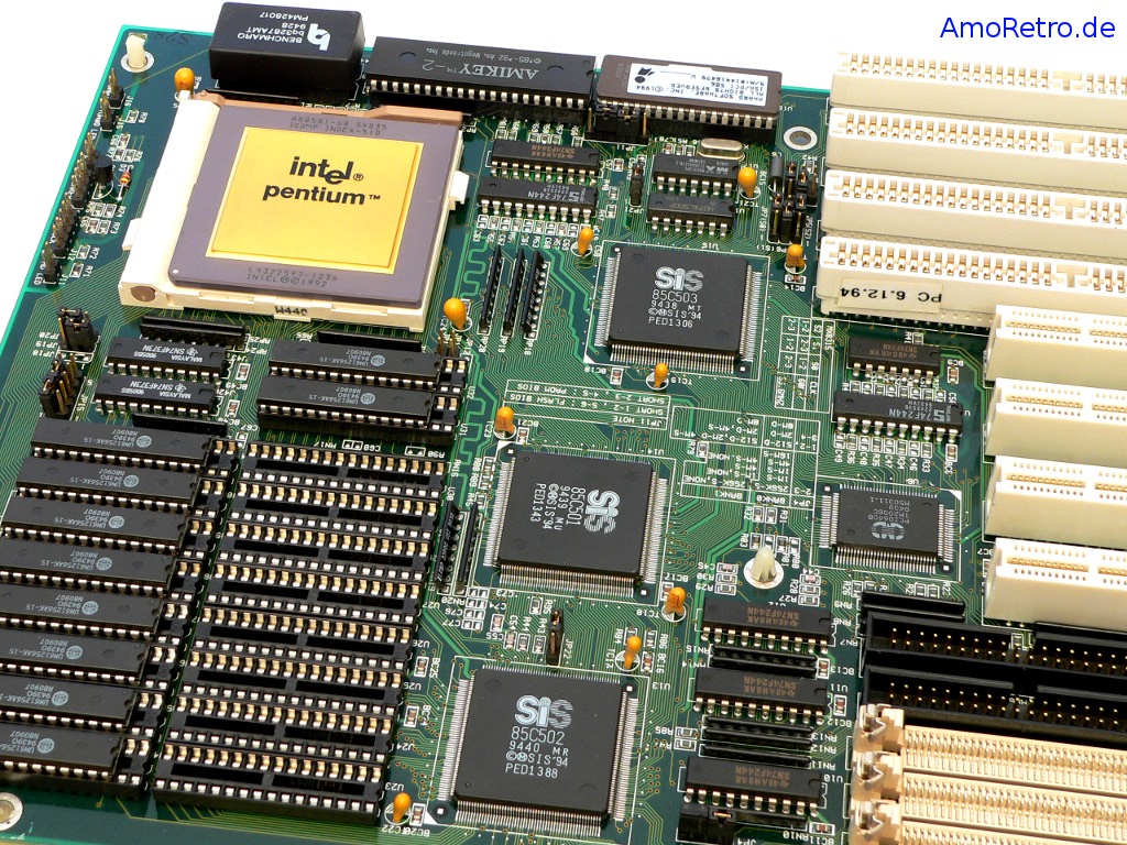 The principle of operation of Hyper-Threading is based on the fact that at any given time only a part of the processor’s resources is used when executing program code. Unused resources can also be loaded with work — for example, one more application (or another thread of the same application) can be used for parallel execution.
HT is not true multiprocessing, because the number of blocks directly executing commands has not changed. Only the efficiency of their use has increased. Therefore, the better a specific program is optimized for HT, the higher the performance gain will be. According to Intel, the advantage of HT can reach 30%, while the blocks that implement it occupy less than 5% of the total area of the Pentium 4 chip. However, even perfectly optimized applications can, for example, access data that is not in the cache -CPU memory, causing it to idle. If the NetBurst architecture itself was designed to increase the number of megahertz, then Hyper-Threading, on the contrary, is designed to increase the work performed per cycle.
One of the reasons for the rather late introduction of Hyper-Threading in Pentium 4 (support exists not only in the Northwood core, but even in Willamette, but was blocked) was the relatively low prevalence of Windows XP — the only OS of the Windows family that fully supports the new technology. Also, the technology must be supported by the chipset and BIOS of the motherboard.
Currently, Hyper-Threading technology is supported by the Pentium 4 3.06 GHz processor with a system bus frequency of 533 MHz, as well as all processors with a bus frequency of 800 MHz.
Celeron
After the release of the Pentium 4 Willamette for Socket 478, in order to force out processors for Socket 370 from the market, and also, wanting to occupy the niche of budget processors (where the Celeron Tualatin was before), Intel releases the Celeron based on the core Willamette 128 .
The Willamette 128 core is architecturally the same as the Pentium 4 Willamette core. The organization of the cache and its algorithms have not changed, the only difference is the size — 128 KB cache in the second level instead of 256 KB in the original Pentium 4 Willamette.
Naturally, the Socket 478 form factor, which Intel is going to use for a long time, has been retained. Thus, Intel transfers its processors to one platform, so that with a subsequent upgrade, it will not be necessary to change the motherboard along with the processor.
On May 15, 2002, the first processor called Celeron, built on the basis of Pentium 4, with a frequency of 1.7 GHz, appears. Later, on June 12, 2002, a 1.8 GHz version appears.
The new Celeron, as before, uses a 100 MHz system bus, but now with the transmission of 4 signals per clock. The quad 100 MHz system bus finally solves the old Celeron problem of lack of FSB bandwidth.
Like the Pentium 4 Willamette, the new Celeron is made using 0.18 microns. technical process. Consists of 42 million transistors. Available with frequencies of 1.7 and 1.8 GHz.
The next and last Celeron core for today is Northwood (of course, with L2 cache reduced to 128 KB). The first processor based on this core was Celeron 2.0 GHz, which was released on September 18, 2002. It, like the Celeron Willamette 128, completely repeats the characteristics of its older brother Pentium 4 Northwood, except for a bus designed exclusively for 400 MHz (4 * 100 MHz) and a 128 KB L2 cache.
Application 0.13 µm. process technology gives the advantage of good overclockability. The Northwood core has a good frequency potential (today up to 3.2 GHz), so there is room for overclocking.
XEON
A little less than three years have passed since the first release of the Intel Pentium II Xeon. And Intel, on May 21, 2001, continuing its course of segmenting its processors, announces the next generation Xeon processor, which is based on the Pentium 4 Willamette core. The processor is called in the old way, Intel Xeon, and is available in three versions: 1. 4 GHz, 1.5 GHz and 1.7 GHz. The processor core is almost completely identical to the regular (desktop) version of the Pentium 4, except for minor details. This means that the new Xeon has everything that the Pentium 4 has — both the advantages of the new architecture and its disadvantages.
The first Xeon models were produced using 0.18 µm. process technology, with a core that almost completely repeated the Pentium 4 Willamette and was codenamed Foster . The processor was produced with clock speeds up to 2.0 GHz. Consisted of 42 million transistors.
L1 cache, like all Pentium 4 processors, with NetBurst architecture, 8 KB data cache. Second level cache — 256 KB with improved data transfer (256 KB Advanced Transfer Cache). Just like the Pentium 4 Willamette, the new Xeon uses a 400 MHz system bus (4 * 100 MHz) that works synchronously with two memory channels at 400 MHz.
Historically, the Intel Xeon processor lines (i.e. Pentium II Xeon, Pentium III Xeon) have always used a different design than conventional processor versions. While the Pentium II and Pentium III processors came in the 242-pin Slot1 variant, their Xeon versions used the 330-pin Slot-2 connector. Most of the extra legs were used to supply the chip with extra power. With two megabytes of L2 cache, the Pentium III Xeon consumed more power than its 256-kilobyte counterpart. A similar situation happened with the new Xeon. While the early Pentium 4 Willamette processors used a 423-pin connector, the Xeon uses a 603-pin interface designed for use in Socket 603. The processor can only work in single or dual processor configurations.
On January 9, 2002, Xeon processors appear, made on the basis of the Northwood core using 0.13 microns. process technology, and equipped with 512 KB L2 cache. The core codename is Prestonia . From its predecessor — Xeon Foster, it differs only in an increased cache and a more advanced technical process. Processors operate at frequencies from 1.8 GHz to 3.0 GHz. Consist of 55 million transistors. Hyper-Threading support appeared in processors with Prestonia core for the first time.
March 12, 2002, the Xeon MP processor is released. Manufactured using 0.18 µm. and is equipped with 256 KB L2 cache. The main difference from the Xeon Foster processors is the ability to work in multiprocessor systems. They operate at frequencies from 1.4 to 1.6 GHz. These processors also support Hyper-Threading technology.
On November 4, 2002, Xeon MP processors made using 0.13 microns appear. technical process. These processors, running at 1.5 GHz, 1.9GHz and 2.0 GHz differ from their fellow Xeon Prestonia not only in the ability to work in multiprocessor configurations, but also in the presence of an integrated L3 cache of 1 or 2 MB. Thanks to this, the number of transistors that make up the processor has increased to 108 million!
On November 18, 2002, Xeon processors operating at 533 MHz (4 * 133 MHz) system bus appeared. These processors are made on the Prestonia core, using 0.13 µm. process technology and consist of 108 million transistors. Cache memory of the second level — 512 KB. Third level cache 1 MB. Xeon processors on the 533 MHz bus are available with clock speeds from 2.0 GHz to 3.06 GHz (released March 10, 2003). A 3.2 GHz processor was also recently announced.
What’s next?
At the end of 2003, Intel will introduce a new core for its processors — Prescott . These processors will be manufactured using 0.09 µm. (90 nm) technology. The Prescott core will consist of 125 million transistors and contain 1 MB of L2 cache. Also, it is possible that the first level cache will finally be increased to 32 KB. Naturally, the new core will have support for Hyper-Threading technology. Only it will already be Hyper-Threading 2 , a further development of «multiprocessing» in a single chip. What will be their difference is not yet known, but there are assumptions (not confirmed by anyone) that the novelty allows you to see not two, but several virtual processors in one physical processor.
A new instruction set will also be added (or an extension of the one already present), including 15 new instructions for converting floating point numbers to integers, complex number arithmetic, special instructions for video decoding, SIMD instructions for floating point format, and a thread synchronization process .
The first processors with this core will run at 3.2 and 3.4 GHz. Their cases will be compatible with those currently used in Northwood Pentium 4 processors. Going forward, Prescott processors will be converted to a new 775-pin LGA 775 package that will require new Socket T motherboards. Only now it is not the same Celeron that it was before. Celeron chips based on the Prescott core will be faster than their predecessors based on Northwood not only due to the increased clock frequency of the core. They will support a system bus with a frequency of 533 MHz, and their cache size will increase from 128 to 256 KB. The first Celerons based on the Prescott core will have frequencies of 2.8 and 3.06 GHz. Not having time to release processors for 90nm technology, Intel is already in full development of the next generation of chip technology — with 65nm standards. Developments are also underway, and there are working chips made using not only 0.065 microns. process technology, but also 45 nm, 32 nm and even 22 nm.
Prescott will be followed by the Tejas core with a 1066 MHz bus. It will be based on eight different processors with clock speeds from 6 to 9.2 GHz. The appearance of the first of them is planned for sale at the end of 2004. After that, the company will introduce the core Nehalem , which uses a 1200 MHz system bus and allows you to get an operating frequency in excess of 10 GHz. Nehalem will be based on a completely new architecture. It will not be an upgraded Pentium 4 like Prescott and Tejas. It will use the LaGrande hardware protection system, and according to some reports, more advanced multithreading technology will be used. The number of transistors in a chip will be about 150-250 million. Pentium Nehalem should appear in 2005.
Also recently announced a new processor from the Pentium 4 — 9 line0517 Intel Pentium 4 Extreme Edition .
It is equipped with Hyper-Threading technology, runs on a system bus of 800 MHz, has a core clock speed of 3. 2 GHz. But its main difference from the previous Pentium 4s was the presence of a 2 MB L3 cache memory integrated into the crystal! This cache is in addition to the standard 512 KB L2 cache and also runs at the processor core frequency (albeit with much higher latency, since it is asynchronous and is designed to speed up work with data from the most frequently used areas of system memory). Thus, the total new Pentium 4 Extreme Edition has 2.5 MB of cache memory! It is also the only desktop processor with a L3 cache integrated into the core.
The Pentium 4 Extreme Edition processor is positioned by Intel mainly for the gaming market, although its use in productive workstations is not excluded. The new processor uses a core from multiprocessor Xeon MP with integrated L3 cache. It was slightly changed in order to support the 800 MHz system bus, reduce power consumption, etc., and packaged in a standard Pentium 4 case.0003
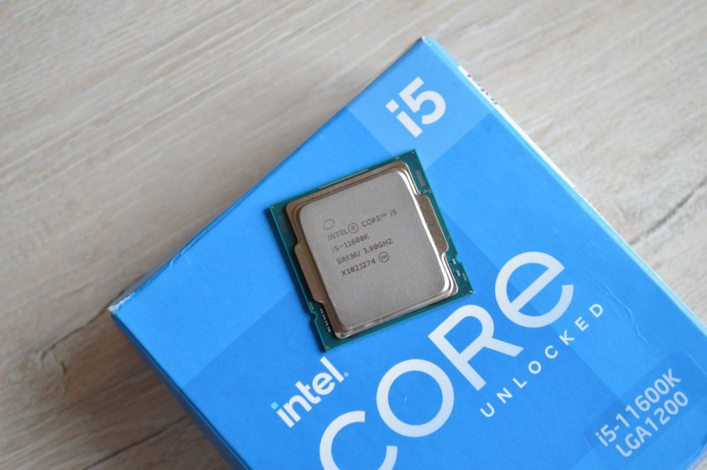 ru
ru Alexey Gavrilenko aka [-Alex-]
Subscribe to our channel in Yandex.Zen or telegram channel @overclockers_news — these are convenient ways to follow new materials on the site. With pictures, extended descriptions and no ads.
Comparison of Intel Pentium D 915 and Intel Pentium 4 HT 630
Comparative analysis of Intel Pentium D 9 processors15 and Intel Pentium 4 HT 630 for all known characteristics in the categories: General Information, Performance, Memory, Compatibility, Security and Reliability, Technology, Virtualization.
Analysis of processor performance by benchmarks: PassMark — Single thread mark, PassMark — CPU mark, Geekbench 4 — Single Core, Geekbench 4 — Multi-Core.
Intel Pentium D 915
versus
Intel Pentium 4 HT 630
Benefits
Reasons to choose Intel Pentium D 915
- Newer processor, release date difference 1 year(s) 5 month(s)
- 1 more core, ability to run more applications simultaneously: 2 vs 1 65 nm vs 90 nm0029
- Approximately 7% improvement in Geekbench 4 — Single Core performance: 179 vs 168
- Approx.
July 2006 vs February 2005 Number of cores 2 vs 1 Process 65 nm vs 90 nm Level 2 cache 4096 KB vs 2048 KB Maximum number of processors in configuration
2 vs 1 Geekbench 4 — Single Core 179 vs 168 Geekbench 4 — Multi-Core 307 vs 214 Reasons to choose Intel Pentium 4 HT 630
- About 7% more clock speed: 3 GHz vs 2.8 GHz
- About 5% more maximum core temperature: 66.
 6°C vs 63.4°C
 - % less power consumption: 84 Watt vs 95 Watt
About
Maximum frequency 3 GHz vs 2.8 GHz Maximum core temperature 66.6°C vs 63.4°C Power consumption (TDP) 84 Watt vs 95 Watt Benchmark comparison
CPU 1: Intel Pentium D 915
CPU 2: Intel Pentium 4 HT 630Geekbench 4 — Single Core CPU 1 CPU 2 Geekbench 4 — Multi-Core CPU 1 CPU 2 Name Intel Pentium D 915 Intel Pentium 4 HT 630 PassMark — Single thread mark 516 PassMark — CPU mark 441 Geekbench 4 — Single Core 179 168 Geekbench 4 — Multi-Core 307 214 Performance comparison
Intel Pentium D 915 Intel Pentium 4 HT 630 Architecture name Presler Prescott Issue date July 2006
February 2005 Place in the rating 2607 2718 Processor Number 915 630 Series Legacy Intel® Pentium® Processor Legacy Intel® Pentium® Processor Status Discontinued Discontinued Applicability Desktop Desktop Support 64 bit Base frequency 2.  80 GHz
 3.00 GHz Bus Speed 800 MHz FSB 800 MHz FSB Crystal area 162 mm2 135 mm2 Level 1 cache 28KB 28KB Level 2 cache 4096KB 2048KB Process 65nm 90nm Maximum core temperature 63.4°C 66.6°C Maximum frequency 2.  8 GHz
8 GHz 3GHz Number of cores 2 1 Number of transistors 376 million 169 million Permissible core voltage 1.200V-1.3375V 1.200V-1.400V Supported memory types DDR1, DDR2, DDR3 DDR1, DDR2, DDR3 Low Halogen Options Available Maximum number of processors in configuration
2 1 Package Size 37.  5mm x 37.5mm
 37.5mm x 37.5mm Supported sockets PLGA775 PLGA775 Power consumption (TDP) 95 Watt 84 Watt Execute Disable Bit (EDB) Intel® Trusted Execution Technology (TXT) Enhanced Intel SpeedStep® Technology Parity FSB Idle States Intel 64 Intel® AES New Instructions Intel® Demand Based Switching Intel® Hyper-Threading Technology Intel® Turbo Boost Technology Physical Address Extensions (PAE) 32-bit Thermal Monitoring Intel® Virtualization Technology (VT-x) Intel® Virtualization Technology for Directed I/O (VT-d) Pentium | it’s.
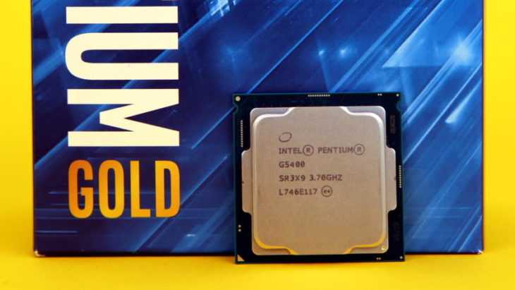 .. What is a Pentium?
Pentium (pronounced: Pentium ) is a trademark of several generations of microprocessors in the Intel family since March 22, 1993. The Pentium is Intel’s fifth generation processor and has replaced the Intel 80486 (often referred to simply as the 486).
Contents
- 1 History
- 2 Alternate history
- 3 Main differences from the 486th processor
- 4 models
- 4.1 P5
- 4.2 P54C
- 4.3 P54CS
- 4.4 P55C
- 4.5 Pentium OverDrive
- 4.6 Tillamook
- 5 Other processors using the Pentium
- 6 Specifications for various cores
- 7 Links
brand
History
Intel Pentium 60, the first model of the Pentium
In June 1989, Vinod Dam made the first sketches of a processor codenamed P5. He did not suspect that this particular product would be one of the main achievements of Intel Corporation.
 At the end of 1991, the design of the processor layout was completed, and engineers were able to run software on it. The stage of topology optimization and work efficiency improvement has begun. February 1992 years of design was basically completed, comprehensive testing of an experimental batch of processors began. In April 1992, a decision was made to start industrial production of processors, and Oregon Factory No. 5 was chosen as the main industrial base. Industrial development of production and final fine-tuning of technical characteristics began. In October 1992, Intel announced that the fifth-generation processors, formerly codenamed P5, would be called Pentium, not 586, as many had assumed. This is due to the fact that many processor manufacturers have actively mastered the production of «clones» (and not only) of the 386 and 486 processors. Intel was going to register the name «586» as a trademark so that no one else could manufacture processors with that name. , however, it turned out that it was impossible to register the numbers as a trademark, so it was decided to name the new processors «Pentium» (from « pent — «- five), which also indicated the generation of this processor.
 On March 22, 1993, a presentation of a new microprocessor took place, a few months later the first computers based on them appeared.
 Alternate History
The story about Vinod Dam is the official version of Intel, but there is another version of the appearance of this processor. In the 1980s, in Russia, Vladimir Mstislavovich Pentkovsky, who worked at the Russian Academy of Sciences under the leadership of Babayan, worked on the Elbrus processor. Around 19On the 89th, a delegation from Intel visited the Computer Science Laboratories of the Russian Academy of Sciences, where they met with Pentkovsky. Pentkovsky received an invitation to come to the United States to exchange experience at the Intel Research Center. Pentkovsky did not return from this trip to Russia, and a few months later Intel officially announced the development of a fundamentally new processor called the Pentium (named after the developer).
Main differences from the 486th processor
- Superscalar architecture.
 Thanks to the use of superscalar architecture, the processor can execute 2 instructions per 1 cycle. This possibility exists due to the presence of two conveyors — u- and v-conveyor. u-pipeline — the main one, performs all operations on integers and real numbers; v-pipeline — auxiliary, performs only simple operations on integers and partially on real ones. In order for older programs (for 486) to take full advantage of the possibilities of this architecture, they had to be recompiled. Pentium is the first
- 64-bit data bus. Allows the Pentium processor to exchange twice as much data with RAM as 486 in one bus cycle (at the same clock speed).
- Branch address prediction mechanism. Used to reduce pipeline idle time caused by instruction fetch delays when the address counter changes while branching instructions are executing. To do this, the processor uses the branch address buffer BTB (Branch Target Buffer), which uses branch address prediction algorithms.
- Separate code and data caching.
 Pentium processors use a 16Kb L1 cache, divided into 2 segments: 8Kb for data and 8Kb for instructions. This improves performance and allows double caching to be available more often than was previously possible. In addition, the caching mechanism has been changed.
 - Improved floating point unit (FPU, coprocessor).
- Symmetric multiprocessing (SMP).
Models
Initially (March 22, 1993) only two models were introduced, based on the P5 core with frequencies of 60 and 66 MHz. However, more efficient Pentium processors were later released, but based on improved cores. In addition, mobile versions of processors and Pentium OverDrive processors were presented.
| Core codename | P5 | P54C | P54CS | P55C | |||||||||
|---|---|---|---|---|---|---|---|---|---|---|---|---|---|
| Process (nm) | 800 | 600 | 350 | ||||||||||
| Clock speed cores (MHz) |
60 | 66 | 75 | 90 | 100 | 120 | 133 | 150 | 166 | 200 | 166 | 200 | 233 |
| Announced | March 23, 1993 | 1994 | March 7, 1994 | March 27, 1995 | June 12, 1995 | January 4, 1996 | June 10, 1996 | January 8, 1997 | June 2, 1997 | ||||
P5
First generation Pentium processors. The two (only) models were announced on March 23, 1993 and ran at 60 MHz and 66 MHz core clocks, the system bus (FSB) was equal to the core frequency, i.e. the core multiplier was «1.0». The second-level cache was located on the motherboard and could be up to 1 MB in size. The processor was produced in a 273-pin CPGA package and installed in a Socket 4 package and operated at 5 V. All Pentium processors are SL Enhanced, which means that they have an SMM system that provides reduced power consumption. Early versions of processors with frequencies of 60-100 MHz (P5 and P54C cores) had a bug in the FPU (math coprocessor), which, in rare cases, led to a decrease in the accuracy of the division operation. This defect was discovered in Lynchburg (USA, Virginia) on 1994 and became known as the «Pentium FDIV bug». Processors on the P5 core were manufactured using the 800 nanometer process technology, according to the bipolar F0 0f c7 c8) of the first generation Pentium processors, they were not advised to buy these models.
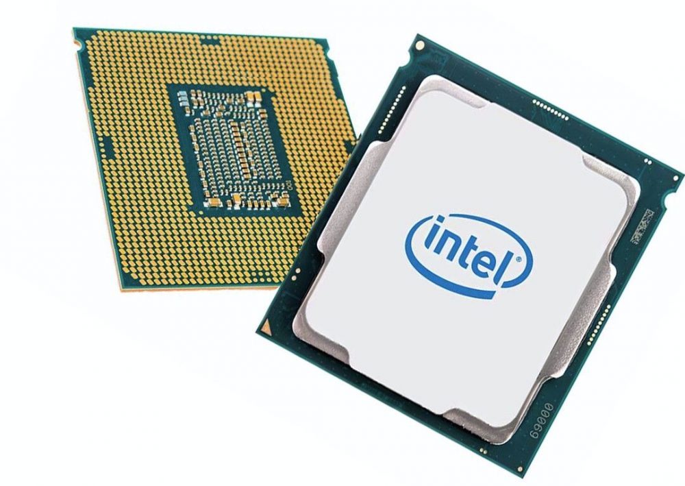 Production had to be stopped for a while. However, the production of improved processors based on the P54C core soon began ….
P54C
On March 7, 1994, the second generation Pentium processors were released. Initially, models were released with clock speeds of 90 and 100 MHz, but then a model with a frequency of 75 MHz was released. The processors were manufactured using 600 nm bipolar BiCMOS technology, which made it possible to reduce the die size to 148 mm² (the core contained 3.2 million transistors) and reduce power consumption to 10.1 W (for the Pentium 100). The supply voltage was also reduced to 3.3 V, the current consumed by the processor is 3.25 A. The processor was produced in a 296-pin CPGA package and installed in Socket 5 or Socket 7 and was not compatible with Socket 4. These processors have improved SMM system, added advanced programmable interrupt controller
P54CS
The first processors based on this core were released on March 27, 1995. By and large, this core is a P54C core manufactured using 350 nm bipolar BiCMOS technology, which made it possible to further reduce the core die size to 91 mm² (Pentium 120 and 133 processors), but soon, as a result of core optimization, its size was reduced to 83 mm² with the same number of transistors. At the same time, the Pentium 200 consumed a current of 4.6 A, and its maximum dissipated energy (heat dissipation) was 15.5 W.
| Multiplier | Processor |
|---|---|
| 1.5 | Pentium 75, Pentium 90, Pentium 100 |
| 2.0 | Pentium 120, Pentium 133 |
| 2.5 | Pentium 150, Pentium 166 |
| 3.0 | Pentium 200 |
P55C
Pentium MMX processor. Top view
On January 8, 1997, Pentium processors based on the third generation P5 core (P55C) were released. The Intel R&D Center in Haifa (Israel) added a new set of instructions to the P55C core called the Pentium MMX). The new processor includes an MMX device with command pipeline processing, L1 cache increased to 32 KB (16 KB for data and 16 KB for instructions). The new processor consists of 4.5 million transistors and is manufactured using advanced 350nm CMOS technology using silicon semiconductors, operates at a voltage of 2.8V. MMX). The die area of Pentium MMX processors is 141 mm². Processors were released in 296-pin CPGA or PPGA package for Socket 7.
Pentium OverDrive
Several generations of Pentium OverDrive were released.
- In 1995, the first Pentium OverDrive was released (using the P24T core). It was designed for installation in sockets such as Socket 2 or Socket 3 and worked with a supply voltage of 5 V, that is, it served to upgrade systems using the 486 processor without replacing the motherboard. At the same time, this processor had all the functions of the first generation Pentium processor (on the P5 core).
 Two models were released, operating at frequencies of 63 MHz and 83 MHz, the older one consumed a current of 2.8 A and had a power dissipation of 14 watts. Due to the high cost, this processor left before it appeared. And although after some time (March 4, 1996), these processors were replaced by Pentium ODP5V with frequencies of 120 and 133 MHz, based on the P5T core (in fact, it is the P54CS core), they also did not become popular.
 - March 4, 1996 the next version of Pentium OverDrive (Pentium ODP3V) is released on the P54CT core. This kernel is based on the P54CS kernel. The processor was available in a 320-pin CPGA package for Socket 5 or Socket 7.
- On March 3, 1997, two Pentium ODPMT models (with frequencies of 150 and 166 MHz) based on the P54CTB core (analogous to P55C) are released, later, on August 4, 19In 1997, two more models came out on the same core (with frequencies of 180 and 200 MHz). They were produced in 320-pin CPGA packages and were designed for Socket 5 or Socket 7 (Pentium ODPMT-200 MMX for Socket 7 only).
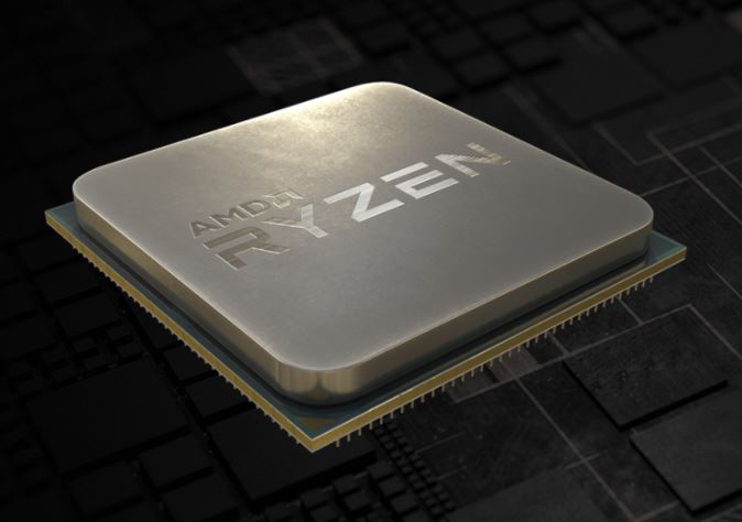
Tillamook
Processors based on this core were intended for portable computers. The Tillamook core (named after a city in Oregon, USA) is a reduced voltage P55C core — the 300 MHz model ran at 2.0 V, drew 4.5 A, and had a thermal output of 8.4 W. Older models (with a frequency of 233, 266 and 300 MHz) were produced using a 250 nm process technology and had a crystal with an area of 90 mm², the younger ones (133 and 150 MHz) using the 280 nm process technology and had a 140 mm² die, the rest were produced using both process technologies. Depending on the case type (TCP or CBGA), the processor was either soldered to the motherboard, or installed in a special MMC1 module. The first models were released in January 1997.
Other processors using the Pentium
brand
Intel Pentium processors were very popular, and Intel decided not to abandon the Pentium brand, naming subsequent processors as well, although they were very different from the first Pentiums and did not belong to the fifth generation. These are:
|
|
|
|
Specifications for various cores
| P5 | P54C | P54CS | P55C | |
|---|---|---|---|---|
| Announcement date of the first model | March 23, 1993 | March 7, 1994 | March 27, 1995 | January 8, 1997 |
| Clock frequencies, MHz | 60, 66 | 75, 90, 100 | 120, 133, 150, 166, 200 | 166, 200, 233 |
| System bus frequency (FSB), MHz | 60, 66 | 50, 60, 66 | 60, 66 | 66 |
| L1 cache, KB | 8 (for data)+8 (for instructions) | 16+16 | ||
| L2 cache, KB | external up to 1 MB | |||
| Supply voltage, V | 5 | 3. 3 3 |
2.8/3.3 | |
| Number of transistors, million | 3.1 | 3.2 | 3.3 | 4.5 |
| Chip area, mm² | 294 | 148 | 90 | 141 |
| Maximum heat dissipation, W | 16 | 10.1 | 15.5 | 16 |
| Process technology, nm | 800 | 600 | 350 | |
| Connector | Socket 4 | Socket 5, Socket 7 | Socket 5, Socket 7 (150-200 — Socket 7 only) | Socket 7 |
| Housing | 273-pin PGA | 296-pin CPGA | 296-pin CPGA/PPGA | |
| Addressable memory | 4 GB | |||
| Register capacity | 32 | |||
| External bus width | 64 | |||
| Address bus width | 32 | |||
Links
- Detailed list of Pentium processors with photos
- Pentium Processor Documentation
- Electrical parameters of processors, in particular Intel Pentium (English)
- Detailed specifications for processors
16 Intel innovations that have changed our lives
May 13, 2021DevicesTechnologies
Intel has been a pioneer in the IT industry for more than 50 years. Thanks to its revolutionary developments, we can use Wi-Fi at home, in the office, even in the subway, take thin and light laptops to study or on business trips and not get lost in the electronics store, choosing a new computer model. We tell you what other innovations Intel has brought to the world of technology and our lives.
Share
0
1965: Moore’s law
Intel was incorporated in 1968, but three years before that, Gordon Moore, one of the future founders, noticed an interesting pattern. New chips hit the market every 12 months, and the number of transistors in the next generation doubled. This empirical observation about the exponential growth in the power of devices later became known as Moore’s Law.
The engineer himself, businessman and honorary chairman of the board of directors of Intel, 10 years later, conducted a new market analysis and revised the deadline: the number of transistors doubled every 24 months. Now, with the development of technology, this gap is gradually decreasing, but still Moore’s law remains one of the pillars of IT.
1970: dynamic memory
Image: Oleksandr Lysenko / Mirage_studio / Tanya Repina
Before Intel, computer systems used magnetic or ferrite core memory. But its production required painstaking manual labor, and significant power was needed to power it.
The Intel® 1101 and 1103 DRAMs revolutionized the industry. Within a few years, these compact solutions almost completely ousted ferrite modules from the market, and over time, only memories remained of the former type of memory.
1971: The first CPU in a single chip
Intel engineer Ted Hoff came up with the idea to combine all the chips into one chip. This is how the world’s first microprocessor Intel® 4004 appeared — it was created for Japanese calculators Busicom 141-PF.
The Intel 4004 included 2,300 transistors and was comparable in performance to an ENIAC computer with 38,000 vacuum tubes. This car occupied 167 sq. m of area, weighed 30 tons and generated 174 kW of heat, and the dimensions of the Intel 4004 microprocessor were 4 x 3 mm², it worked at a frequency of up to 740 kHz and generated 1 W of heat.
The Intel 4004 was the first commercially successful processor. The legend turns 50 this year.
1974: microprocessor instead of bulky computers
In the mid-70s, computers cost several thousand dollars and were available mainly to the military or scientists. Chips were developed for specific tasks: as the basis for a calculator, industrial equipment or a communication device.
The first general-purpose microprocessor, the Intel® 8080, was offered for as little as $360, and a matchbox-sized chip seemed fantastic to many. Engineers could customize it for different tasks, and if necessary, reprogram it for a new system.
Modern laptops are becoming lighter, sleeker and faster every year. Models based on the Intel® Evo™ platform include the latest 11th Gen Intel® Core™ processors. They are 40% faster than devices released just a couple of years ago and boot in a second. This technique is universal: suitable for comfortable work, resource-demanding games, other entertainment and creativity.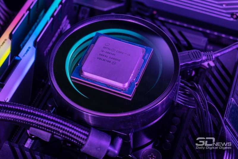
View Intel® Evo™ Notebooks
1978: The Legendary x86
Engineer Stephen Morse laid the foundation for the x86 processor architecture that is still in use today. He first developed this instruction set for the Intel® 8086 microprocessor in just three months, without even realizing how popular the technology would become.
Modern x86 processors support the original instruction set for the 16-bit processor. The term x86 itself appeared only in 1985, with the release of the 32-bit Intel® i80386 chip.
1980: Ethernet
The Ethernet protocol for packet data transfer between devices for computer and industrial networks was born in 1973 by Xerox engineer Robert Metcalfe. The developer had to spend more than 7 years to, with the support of Intel, Xerox and DEC, develop standards for this technology and ensure its widespread adoption.
Manufacturers soon realized the potential of the protocol and began mass-producing equipment to work with it. This allowed Ethernet to supplant the former Token ring and ARCNET protocols, survive hundreds of updates, and remain in demand for more than four decades.
1993: Intel® Pentium® and 100 million operations per second
The first Intel Pentium processor with 3.1 million transistors was released — it was 1,500 times faster than the Intel 4004 and replaced the «four» (Intel® 80486, which often referred to simply as 486). Due to the superscalar two-pipeline architecture, it executed two instructions in one cycle.
The first Pentium was followed by Intel Pentium Pro, MMX and other modifications, and then new generations of processors. They have long been entrenched in the market and have become the basis of billions of affordable home PCs.
1995: USB
Image: Oleksandr Lysenko / Mirage_studio / Tanya Repina
Together with other industry giants, Intel has developed the most popular bus for connecting peripherals. Actually, USB stands for Universal Serial Bus — «Universal Serial Bus».
The technology made it possible to simultaneously exchange data and provide power to the device. USB helped not only to abandon additional connectors, but also to simplify the connection — it provided a real plug & play without a long installation of drivers and gadget settings.
2001: the first 64-bit processor
It became clear that 32-bit memory addressing was no longer enough. That’s why Intel released the 64-bit Itanium® processor for servers and industrial systems.
Later, 64-bit processors were also used in the consumer segment. They allow you to address 1,019 memory addresses, and even NASA computers have enough for now.
2005: Multi-core processors
Intel® Pentium® D was introduced, which included two cores instead of one for more efficient parallel computing. They became the first x86-64 multi-core processors for personal computers.
Today, many smartphones are equipped with 8-core processors. And research chips can include dozens of cores: for example, in 2006, Intel showed the 80-core Polaris.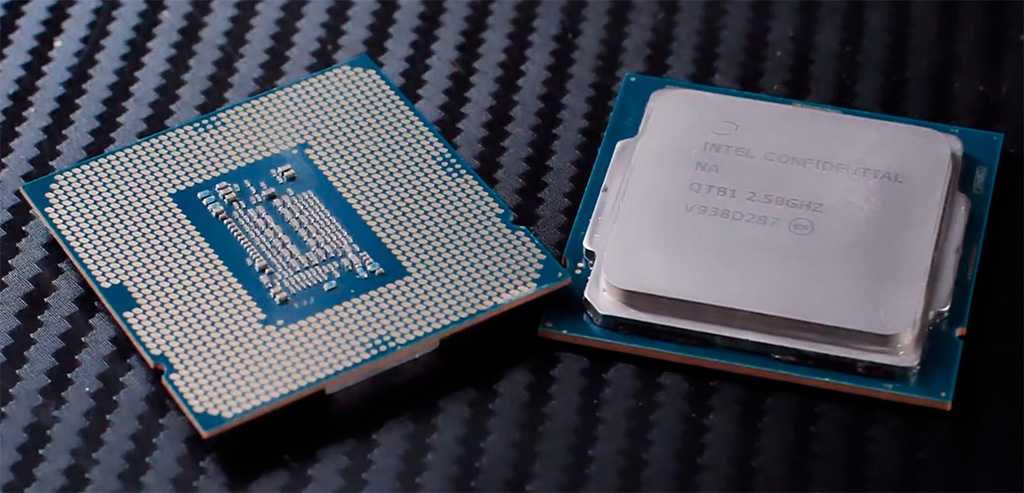 The Intel Pentium D is the starting point for these solutions.
2010: Intel® Turbo Boost™ Technology
Intel figured out how to automatically switch between economy and high performance and introduced Intel Turbo Boost Technology. The fact is that PC processors do not always need to work at the limit of power. For example, when a user listens to music or chats in a messenger, the system should not use all the features. At the same time, in resource-intensive games at maximum settings, you need to “turn on all engines”.
Intel Turbo Boost raises the processor’s operating frequency and delivers extreme power for demanding tasks, while keeping power consumption low the rest of the time.
2011: 3D transistors
Initially, transistors were made planar (flat). The 3D model made it possible to increase performance without increasing the supply voltage.
The first 3D chips to market using Intel® 3D Tri-Gate Technology are microprocessors based on the Ivy Bridge architecture..jpg) They consumed 50% less energy than their predecessors and showed a 37% increase in performance.
They consumed 50% less energy than their predecessors and showed a 37% increase in performance.
2011: Ultrabook™ as a trademark
Today we know that an ultrabook is a thin, light and powerful business laptop. We also owe the appearance of this term to Intel: the concept of an ultrabook was presented at the Intel Developer Forum 2011 in San Francisco.
Technically, Ultrabook is a trademark owned by Intel. Prior to this, such gadgets were called subnotebooks, but the term did not take root.
Ultrabooks had to meet certain criteria, which were updated annually. First of all, they had to be built on the basis of energy-efficient Intel processors, include an SSD (solid state drive) for fast loading of the operating system and programs, and have a long enough battery life.
2015: Intel® 3D XPoint (Intel® Optane™)
Intel 3D XPoint technology was born, enabling the creation of particularly fast storage media, faster than NAND and larger than DRAM. Intel releases them under the Intel Optane brand.
Now such drives are often used in laptops so that the system boots instantly. They are also installed in servers that should provide maximum performance.
2019: Chips with Intel® Wi-Fi Technology 6
Processors with support for the new data transfer standard began to be installed in thin and light laptops. This technique is chosen by business users who often have to work in Wi-Fi networks with a large number of connections, for example, in business centers, coworking spaces, and airports.
Devices with Intel Wi-Fi 6 can reduce latency by up to 75% compared to Wi-Fi 5 and quadruple network capacity. In practice, this means a fourfold increase in throughput in congested areas.
2021: Intel® Evo™ Platform
The new Intel Evo Platform Compliance Verification Program has been released and sets strong technical criteria for notebook manufacturers, including performance in real world scenarios and applications.