All Products | Schneider Electric India
-
Low Voltage Products and Systems
-
Building Automation and Control
-
Medium Voltage Distribution and Grid Automation
-
Critical Power, Cooling and Racks
-
Industrial Automation and Control
-
Access to Energy
-
Solar and Energy Storage
Top Ranges
Top Ranges
Top Ranges
Top Ranges
Top Ranges
Top Ranges
Top Ranges
Top Ranges
-
Ranges: 36
-
Ranges: 9
-
Ranges: 29
-
Ranges: 23
-
Ranges: 14
-
Ranges: 44
-
Ranges: 26
-
Ranges: 2
-
Ranges: 36
All Products | Schneider Electric India
-
Building Automation and Control
-
Medium Voltage Distribution and Grid Automation
-
Critical Power, Cooling and Racks
-
Industrial Automation and Control
-
Access to Energy
-
Solar and Energy Storage
Top Ranges
Top Ranges
Top Ranges
Top Ranges
Top Ranges
Top Ranges
Top Ranges
Top Ranges
-
Ranges: 36
-
Ranges: 9
-
Ranges: 29
-
Ranges: 23
-
Ranges: 14
-
Ranges: 44
-
Ranges: 26
-
Ranges: 2
-
Ranges: 36
L1, L2 and L3 cache.
 Definition — Iron on DTF
24736
views
The original is here.
Any computer processor, cheap laptop or million dollar server has a cache everywhere. And it has several levels.
Must be an important component, otherwise why is it there? What does the cache do, and why does it need several levels? What does 12-position associativity actually mean?
What is a cache?
In a nutshell: This is a small but very fast memory that sits next to the logical blocks of the processor.
But of course we want to know a lot more about the cache…
Imagine an imaginary magical storage system: it’s unrealistically fast, it can handle an infinite number of concurrent operations, and it always keeps data safe. If at least something remotely similar to this existed, then the design of processors would be much simpler.
The processor would only need logic modules for addition, multiplication, etc., and a system to handle the data transfer.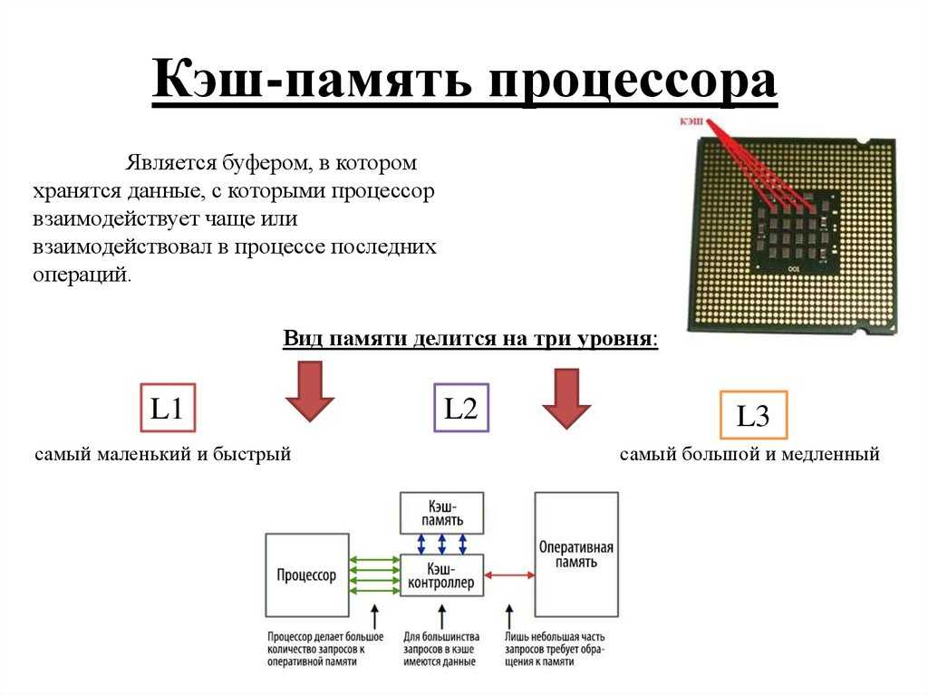 This is due to the fact that our theoretical data storage system can send and receive all the necessary numbers instantly; none of the logical blocks will be waiting for data transfer.
But as we all know, there is no magic storage technology. Instead, we have hard drives (HDD) or solid state drives (SSD) and even the best of them are not capable of handling all the data transfers required by a conventional processor.
Great data storage elephant.
The reason modern processors are so fast is that they only need one clock cycle to add two 64-bit integer values together. For a chip with a frequency of 4 GHz, this process will take only 00000000025 seconds, or a quarter of a nanosecond.
Meanwhile, hard drives take thousands of nanoseconds to find the data, not to mention that it still needs to be transferred. And solid-state drives — tens or hundreds of nanoseconds.
Disks of this kind cannot be built into the processor, this is understandable. Otherwise, they would be physically separated. This, in turn, would only increase the time for data transfer.
The second great data storage elephant, unfortunately.
Therefore, we need another storage system that sits between the processor and the main storage. It needs to be faster than a disk, as well as be able to process a lot of data at the same time, and be much closer to the processor.
Well, we already have such a system — random access memory (RAM). And this is its main task.
Virtually all «RAM» consists of dynamic random access memory (DRAM). It is much faster than any other disk.
Although DRAM is very fast, the amount of memory leaves much to be desired.
Micron’s largest DDR4 memory chips capable of storing 32 Gb or 4 GB of data. At the same time, the most capacious hard drives have a capacity of 4000 times more.
Thus, although we have increased the data transfer rate, we need to understand what is required for the processor in the first place, because the memory is very limited. These solutions are handled by hardware and software.
At least DRAM can be produced in a chip package (embedded DRAM). But the processors are quite small, so there is no way to insert a lot of memory.
10 MB RAM. To the left of the Xbox 360 GPU.
The vast majority of DRAM is located right next to the processor, which in turn is connected to the mat. board. The closest component to the processor, and yet not fast enough.
DRAM still takes about 100 nanoseconds to find data, but it is capable of transmitting it at billions of bits per second. It seems that we need another link between the processor and DRAM.
SRAM (Static Random Access Memory) enters the scene. Where DRAM uses microscopic capacitors to store data as an electrical charge, SRAM uses transistors. And they can run almost as fast as logic modules in a processor (about 10 times faster than DRAM).
SRAM has a flaw, and again it’s about size.
Transistor memory takes up much more space than DRAM. 4GB DDR4 is equivalent to only 100MB SRAM. But, since the design of the CPU is similar to SRAM, it can be built into the processor itself, located as close as possible to the logical devices.
Each time you increase the speed, the storage capacity decreases. We could keep adding more sections, each one faster but smaller.
So we’ve come to a more technical definition of what a cache is: These are a few blocks of SRAM that are located inside the processor. They are used to keep the logical blocks busy by sending and storing data at ultra-fast speeds. Satisfied? Well, good. From now on, things get a lot more complicated!
Cache: multilevel parking
As we said, the cache is necessary because the processor does not have a magic storage system that can satisfy the data needs of the logic modules. Modern CPUs and GPUs contain a number of SRAM blocks that are organized into a hierarchy, a sequence of caches that are ordered as follows:
In the image above, the processor is represented by a black dotted rectangle. The ALU (Arithmetic Logic Unit) is on the left. This structure powers the processor and handles the math. Technically, it’s not a cache. The closest memory level to the ALU are the registers (they are grouped into a register file).
Each contains a single number, such as a 64-bit integer. Its value can be a piece of data about something, a specific instruction code, or a memory address of some other data.
The register file in the desktop processor is very small — for example, in the Intel Core i9-9900K there are two «banks» in each core. One for integers, total 180 64-bit registers. Another register file for vectors (small arrays of numbers), 168 256-bit entries. Thus, the total register file for each core is a little less than 7 KB. By comparison, the Nvidia GeForce RTX 2080 Ti streaming multiprocessor (GPU core equivalent) register file size is 256 KB.
Registers are SRAM, like cache, but they are as fast as the ALU they serve, moving data in one clock cycle. But they are not designed to store very large amounts of data (only one part), so there are always several large blocks of memory nearby: this is the 1st level cache.
Intel Skylake processor. An enlarged image of one of the nuclei.
The above image is an enlarged view of one of the Intel Skylake processor cores.
ALU and registry files are visible on the left. They are highlighted in green. At the top of the photo, in the middle, L1 cache is marked in white. It doesn’t have much information, only 32 kB, but like registers, it’s very close to logical blocks and runs at the same speed as them.
Another white rectangle indicates the second level 1 instruction cache, also 32 kB. As the name suggests, it stores various instructions that will be divided into smaller, so-called micro operations (usually labeled as µops). All of them will be transferred to the ALU. They also have a cache, L0, since it is smaller (only 1500 operations) and closer than the L1 cache.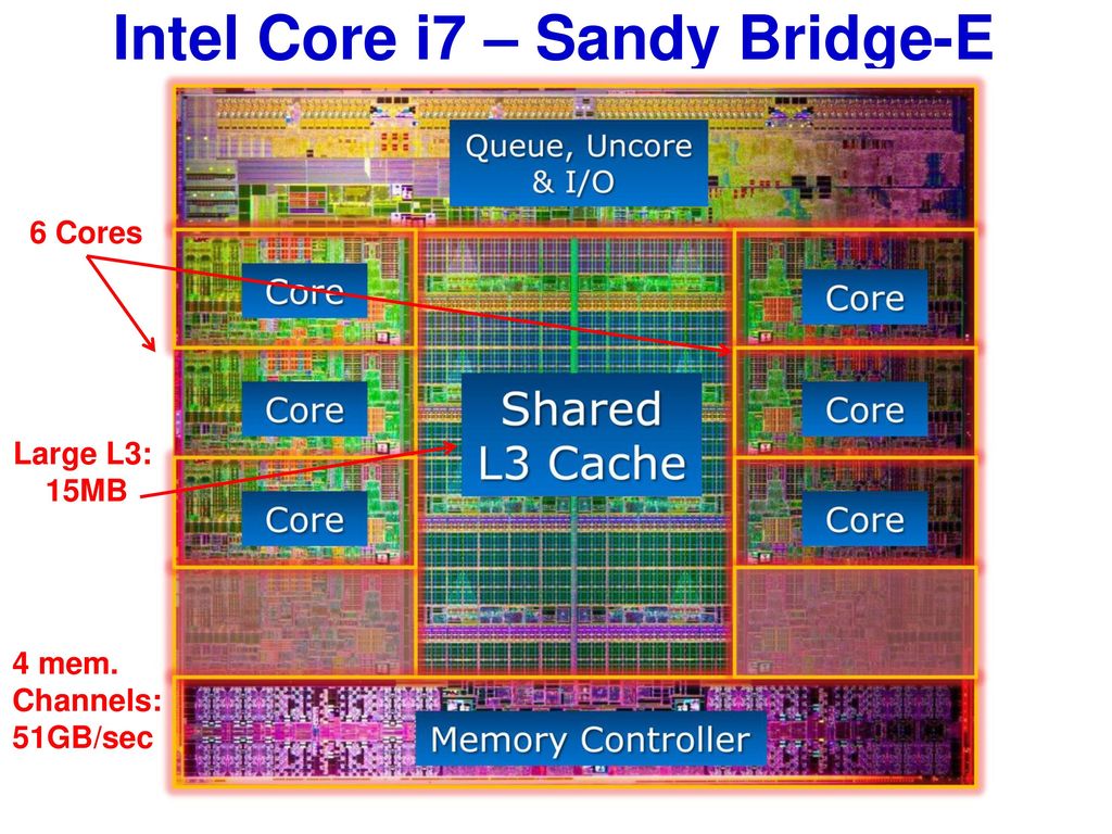
You might be wondering why these SRAM blocks are so small? Why aren’t they measured in megabytes? In sum, the data and instruction caches take up almost as much space on the chip as the main logic blocks. Therefore, increasing their volume would increase the overall size of the matrix.
But the main reason why they contain several KB is that the time required to find and retrieve data increases as the amount of memory increases. The L1 cache needs to be really fast, and so a trade-off between size and speed needs to be made. At best, it takes about 5 cycles (longer for floating point values) to get the data out of this cache ready for use.
L2 cache in Skylake.
If this were the only cache in the processor, its performance would suddenly come to a standstill. So they have another level of memory built into the core: the L2 cache. This is a shared block of memory that stores instructions and data.
It is always slightly larger than level 1: AMD Zen 2 processors, for example, contain up to 512 kB, so the lower level caches are in good condition. However, the additional size incurs a delay in retrieving and transferring data from this cache. It takes about twice as long as in L1.
Remembering the Intel Pentium, then the L2 cache was a separate chip that was located on a small plug-in board (for example, RAM DIMM), or was built into the motherboard. In the end, L2 did get into the processor case. Integration into the processor matrix, based on Pentium III and AMD K6-III chips.
Further development entailed another layer to support other lower levels, and this happened due to the growth of multi-core processors.
Intel Kaby Lake processor.
In this image of Intel Kaby Lake, 4 cores are shown in the middle left (the integrated GPU occupies almost half of the die, on the right). Each core has its own set of level 1 and 2 caches (highlighted in white and yellow, respectively), but they also have a third set of SRAM blocks.
The L3 cache, although it surrounds one core, is completely separate from the others. Each of them can get free access to the contents of someone else’s cache of the 3rd level. It is much larger (from 2 to 32 MB), but also much slower, averaging 30 cycles, especially if the kernel needs to use data that is in a cache block that is some distance away.
Below we see one of the AMD Zen 2 cores: 32 KB L1 cache (white), 512 KB L2 cache (yellow) and a huge 4 MB L3 cache block (red).
AMD Zen 2. One of the cores.
Stop. How can 32 kB physically take up more space than 512 kB? If L1 contains so little data, why is it so much larger than L2 or L3 cache?
More than just a number
The cache improves computer performance by speeding up the transfer of data to LUNs and by storing a copy of frequently used instructions and data nearby. The information stored in the cache is divided into two parts: the data itself and the place where it was originally located in system memory / storage — this address is called the cache tag.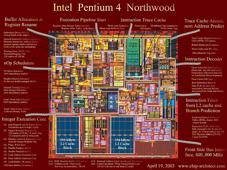
When the processor performs an operation to read or write data from or to memory, it starts by checking the tags in the level 1 cache. If the desired tag is present, then access to this data can be obtained almost immediately. Mismatches occur when the required tag is not at the lowest cache level.
Thus, a new tag is created in the L1 cache, and the rest of the processor takes over the search for data for this tag, through other cache levels (up to the main drive, if necessary). But in order to make room in the L1 cache for this new tag, something else must be loaded into L2.
This results in almost constant data shuffling, all achieved in just a few clock cycles. The only way to achieve this is to have a complex structure around SRAM to manage the data. To put it another way: if the processor core consisted of only one ALU, then the L1 cache would be much simpler, but since there are dozens of them (many of which will pass through two threads with instructions), the cache requires many connections to continue working.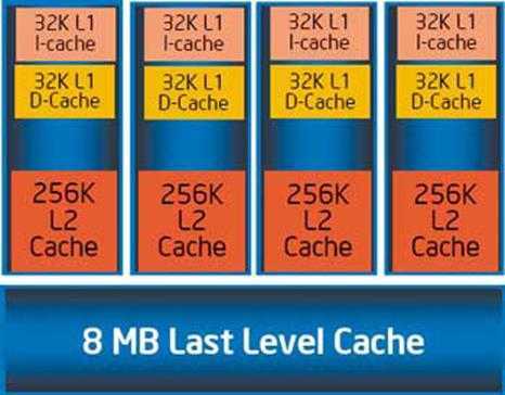
To check the cache in your own processor, you can use free programs such as CPU-Z. But what does all this information mean? An important element is the associative set of labels — it’s all about the rules applied when copying data blocks from system memory to the cache.
The above information is from Intel Core i7-9700K. Its level 1 caches are broken into 64 small blocks called sets, and each of these is further broken down into cache lines (64 bytes in size). An associative set means that a block of data from system memory is mapped to the cache line in one specific set, and not anywhere else.
«x8» tells us that one block can be associated with 8 cache lines in the set. The higher the level of associativity (i.e., the more «ways»), the more likely it is to get a cache hit while the processor is looking for data, and also reduces the number of errors caused by cache misses. The disadvantages include: overall complexity, increased power consumption, and reduced performance as more cache lines must be processed to obtain a data block.
Cache L1+L2 inclusive. L3 cache memory of the victim. Write-back policy, even ECC (error-correcting memory).
Victim cache or Victim buffer (literally Victim cache) is a small specialized cache that stores those cache lines that were recently ousted from the main microprocessor cache when they were replaced.
Another aspect of cache complexity is how data is stored at different levels. The rules are set in a so-called inclusion policy. For example, Intel Core processors have a fully inclusive L1+L3 cache. This means that the same data on the first level can also be on the third. This may seem like a waste of valuable cache memory, but there is a major benefit: if the processor misses a tag lookup at a lower level, it doesn’t have to look it up at a higher level.
On the same processors, the L2 cache is not inclusive: any data stored there is not copied to any other level. This saves space, but results in the processor’s memory system having to look for the missing tag in L3 (which is always much larger). The victim cache is similar, but it is used to store information that comes from a lower level — for example, AMD Zen 2 processors use the L3 victim cache, which simply stores data from L2.
There are other caching policies, such as when data is written to the cache and main system memory. This is called a write policy, and most modern processors use a write-back cache: when data is written to cache memory, there is a delay before system memory is updated with a copy of that cache. For the most part, this pause lasts as long as the data remains in the cache — only after loading does the RAM receive information.
Nvidia GA100 GPU equipped with L1 cache (20MB) and L2 cache (40MB).
For processor designers, choosing the size, type, and policy of caching is a balancing act between advanced chip capabilities and overall increased complexity and required die space. If it were possible to create a 20MB, 1000-way fully associative L1 cache, and not have the chip become the size of Manhattan (and consume the same amount of power), then everyone would have computers with these processors!
The lowest level of caching in modern processors hasn’t changed much in the last decade. However, the L3 cache continues to grow in size. Ten years ago, if you were lucky enough to own a $999 Intel i7-980X, you could get 12MB of L3 cache. For half that amount today, you get 64 MB.
Cache, in a nutshell: an absolutely necessary and amazing technology. We haven’t looked at other types of caches in the CPU and GPU (such as the TLB or texture cache), but since they all follow a simple structure and level pattern, you won’t find it hard to figure them out.
Did you have a computer with a separate L2 cache on the motherboard? What about those Pentium II and Celeron processors (specifically the 300a) that came as daughterboards? Can you remember your first shared L3 processor? Tell us about it in the comments.
Processor cache. Levels and principles of operation
One of the important factors that increase processor performance is the availability of cache memory, or rather its volume, access speed and distribution by levels.
For a long time, almost all processors are equipped with this type of memory, which once again proves the usefulness of its presence.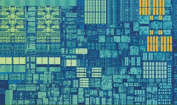 In this article, we will talk about the structure, levels and practical purpose of cache memory, as a very important characteristic of the processor.
What is cache memory and its structure
Cache memory is an ultra-fast memory used by the processor for temporary storage of data that is most often used. This is how, briefly, this type of memory can be described.
Cache memory is built on flip-flops, which, in turn, consist of transistors. A group of transistors takes up much more space than the same capacitors that make up RAM. This entails many difficulties in production, as well as restrictions in volumes. That is why cache memory is a very expensive memory, while having negligible volumes. But from such a structure, the main advantage of such a memory follows — speed. Since flip-flops do not need regeneration, and the delay time of the gate on which they are assembled is small, the switching time of the flip-flop from one state to another is very fast. This allows the cache memory to operate at the same frequencies as modern processors.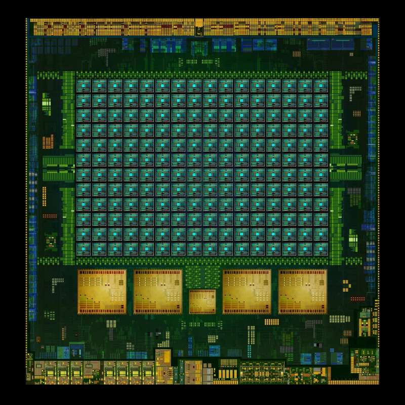
Also, an important factor is the location of the cache. It is located on the processor chip itself, which significantly reduces the access time to it. Previously, cache memory of some levels was located outside the processor chip, on a special SRAM chip somewhere on the motherboard. Now, in almost all processors, the cache memory is located on the processor chip.
What is CPU cache used for?
As mentioned above, the main purpose of cache memory is to store data that is frequently used by the processor. The cache is a buffer into which data is loaded, and despite its small size (about 4-16 MB) in modern processors, it gives a significant performance boost in any application.
To better understand the need for cache memory, let’s imagine the memory organization of a computer as an office. RAM will be a cabinet with folders that the accountant accesses periodically to retrieve large blocks of data (that is, folders). And the table will be the cache memory.
There are elements that are placed on the accountant’s desk, which he refers to several times during an hour. For example, it can be phone numbers, some examples of documents. These types of information are right on the table, which, in turn, increases the speed of access to them.
In the same way, data can be added from those large data blocks (folders) to the table for quick use, for example, any document. When this document is no longer needed, it is placed back in the cabinet (in RAM), thereby clearing the table (cache) and freeing this table for new documents that will be used in the next period of time.
Also with the cache memory, if there is some data that is most likely to be re-accessed, then this data from the RAM is loaded into the cache memory. Very often, this happens with the joint loading of the data that is most likely to be used after the current data. That is, there are assumptions about what will be used «after». These are the simple principles of operation.
Processor cache levels
Modern processors are equipped with a cache that often consists of 2 or 3 levels. Of course, there are exceptions, but this is often the case.
In general, there can be such levels: L1 (first level), L2 (second level), L3 (third level). Now a little more about each of them:
First level cache (L1) is the fastest cache memory level that works directly with the processor core, thanks to this tight interaction, this level has the shortest access time and operates at frequencies close to the processor . It is a buffer between the processor and the second level cache.
We will be looking at volumes on a high performance Intel Core i7-3770K processor. This processor is equipped with 4 x 32 KB L1 cache 4 x 32 KB = 128 KB. (32 KB per core)
Second level cache (L2) — the second level is larger than the first, but as a result, it has lower «speed characteristics». Accordingly, it serves as a buffer between the L1 and L3 levels.