Intel Core i5-4200U vs Nvidia Tegra 4: What is the difference?
33points
Intel Core i5-4200U
34points
Nvidia Tegra 4
Comparison winner
vs
64 facts in comparison
Intel Core i5-4200U
Nvidia Tegra 4
Why is Intel Core i5-4200U better than Nvidia Tegra 4?
- Supports 64-bit?
- 667MHz higher ram speed?
1600MHzvs933MHz - 6nm smaller semiconductor size?
22nmvs28nm - 12GB larger maximum memory amount?
16GBvs4GB - Has AES?
- Uses multithreading?
- Has AVX?
- Has F16C?
Why is Nvidia Tegra 4 better than Intel Core i5-4200U?
- 2.37x faster CPU speed?
4 x 1.9GHzvs2 x 1.6GHz - 472MHz faster GPU clock speed?
672MHzvs200MHz - 1.5MB bigger L2 cache?
2MBvs0.5MB - 128KB bigger L1 cache?
256KBvs128KB - 0.
25MB/core more L2 cache per core?
0.5MB/corevs0.25MB/core - Has TrustZone?
Which are the most popular comparisons?
Intel Core i5-4200U
vs
Intel Celeron N3060
Nvidia Tegra 4
vs
Nvidia Tegra K1 (64-bit)
Intel Core i5-4200U
vs
AMD A6-5200
Nvidia Tegra 4
vs
Qualcomm Snapdragon 888
Intel Core i5-4200U
vs
Intel Core i3-7100
Nvidia Tegra 4
vs
Qualcomm Snapdragon 865 Plus
Intel Core i5-4200U
vs
AMD A6-5350M
Nvidia Tegra 4
vs
Nvidia Tegra 3 T33
Intel Core i5-4200U
vs
Intel Celeron N3350
Nvidia Tegra 4
vs
Nvidia Tegra K1 (32-bit)
Intel Core i5-4200U
vs
AMD A8-5550M
Nvidia Tegra 4
vs
ARM Cortex-A53
Intel Core i5-4200U
vs
Intel Core i5-1135G7
Nvidia Tegra 4
vs
Qualcomm Snapdragon 835
Intel Core i5-4200U
vs
AMD A10-5750M
Nvidia Tegra 4
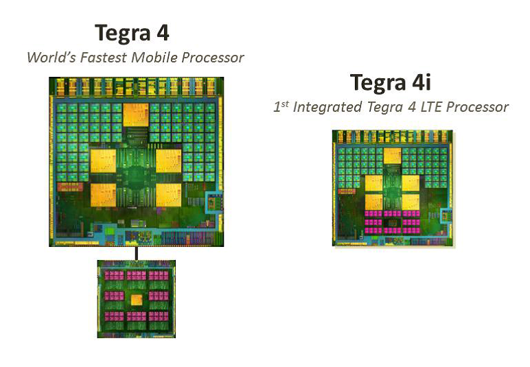
vs
Nvidia Tegra 4i
Intel Core i5-4200U
vs
Intel Celeron N4020
Nvidia Tegra 4
vs
Qualcomm Snapdragon S4 Pro MSM8960T
Intel Core i5-4200U
vs
Intel Pentium G3430
Nvidia Tegra 4
vs
Apple A14 Bionic
Price comparison
User reviews
Performance
1. CPU speed
2 x 1.6GHz
4 x 1.9GHz
The CPU speed indicates how many processing cycles per second can be executed by a CPU, considering all of its cores (processing units). It is calculated by adding the clock rates of each core or, in the case of multi-core processors employing different microarchitectures, of each group of cores.
2.CPU threads
More threads result in faster performance and better multitasking.
3.turbo clock speed
2.6GHz
Unknown. Help us by suggesting a value. (Nvidia Tegra 4)
When the CPU is running below its limitations, it can boost to a higher clock speed in order to give increased performance.
4.Has an unlocked multiplier
✖Intel Core i5-4200U
✖Nvidia Tegra 4
Some processors come with an unlocked multiplier which makes them easy to overclock, allowing you to gain increased performance in games and other apps.
5.L2 cache
A larger L2 cache results in faster CPU and system-wide performance.
6.L3 cache
Unknown. Help us by suggesting a value. (Nvidia Tegra 4)
A larger L3 cache results in faster CPU and system-wide performance.
7.L1 cache
A larger L1 cache results in faster CPU and system-wide performance.
8.L2 core
0.25MB/core
0.5MB/core
More data can be stored in the L2 cache for access by each core of the CPU.
9.L3 core
1.5MB/core
Unknown. Help us by suggesting a value. (Nvidia Tegra 4)
More data can be stored in the L3 cache for access by each core of the CPU.
Memory
1.RAM speed
1600MHz
933MHz
It can support faster memory, which will give quicker system performance.
2. maximum memory bandwidth
25.6GB/s
Unknown. Help us by suggesting a value. (Nvidia Tegra 4)
This is the maximum rate that data can be read from or stored into memory.
3.DDR memory version
Unknown. Help us by suggesting a value. (Nvidia Tegra 4)
DDR (Double Data Rate) memory is the most common type of RAM. Newer versions of DDR memory support higher maximum speeds and are more energy-efficient.
4.memory channels
More memory channels increases the speed of data transfer between the memory and the CPU.
5.maximum memory amount
The maximum amount of memory (RAM) supported.
6.bus transfer rate
Unknown. Help us by suggesting a value. (Intel Core i5-4200U)
Unknown. Help us by suggesting a value. (Nvidia Tegra 4)
The bus is responsible for transferring data between different components of a computer or device.
7.Supports ECC memory
✖Intel Core i5-4200U
✖Nvidia Tegra 4
Error-correcting code memory can detect and correct data corruption. It is used when is it essential to avoid corruption, such as scientific computing or when running a server.
8.eMMC version
Unknown. Help us by suggesting a value. (Intel Core i5-4200U)
Unknown. Help us by suggesting a value. (Nvidia Tegra 4)
A higher version of eMMC allows faster memory interfaces, having a positive effect on the performance of a device. For example, when transferring files from your computer to the internal storage over USB.
9.bus speed
Unknown. Help us by suggesting a value. (Intel Core i5-4200U)
Unknown. Help us by suggesting a value. (Nvidia Tegra 4)
The bus is responsible for transferring data between different components of a computer or device.
Benchmarks
1. PassMark result
Unknown. Help us by suggesting a value. (Nvidia Tegra 4)
This benchmark measures the performance of the CPU using multiple threads.
2.PassMark result (single)
Unknown. Help us by suggesting a value. (Nvidia Tegra 4)
This benchmark measures the performance of the CPU using a single thread.
3.Geekbench 5 result (multi)
Unknown. Help us by suggesting a value. (Nvidia Tegra 4)
Geekbench 5 is a cross-platform benchmark that measures a processor’s multi-core performance. (Source: Primate Labs, 2022)
4.Cinebench R20 (multi) result
Unknown. Help us by suggesting a value. (Nvidia Tegra 4)
Cinebench R20 is a benchmark tool that measures a CPU’s multi-core performance by rendering a 3D scene.
5.Cinebench R20 (single) result
Unknown. Help us by suggesting a value. (Nvidia Tegra 4)
Cinebench R20 is a benchmark tool that measures a CPU’s single-core performance by rendering a 3D scene.
6.Geekbench 5 result (single)
Unknown. Help us by suggesting a value. (Nvidia Tegra 4)
Geekbench 5 is a cross-platform benchmark that measures a processor’s single-core performance. (Source: Primate Labs, 2022)
7.Blender (bmw27) result
Unknown. Help us by suggesting a value. (Intel Core i5-4200U)
Unknown. Help us by suggesting a value. (Nvidia Tegra 4)
The Blender (bmw27) benchmark measures the performance of a processor by rendering a 3D scene. More powerful processors can render the scene in less time.
8.Blender (classroom) result
Unknown. Help us by suggesting a value. (Intel Core i5-4200U)
Unknown. Help us by suggesting a value. (Nvidia Tegra 4)
The Blender (classroom) benchmark measures the performance of a processor by rendering a 3D scene. More powerful processors can render the scene in less time.
9. performance per watt
Unknown. Help us by suggesting a value. (Intel Core i5-4200U)
Unknown. Help us by suggesting a value. (Nvidia Tegra 4)
This means the CPU is more efficient, giving a greater amount of performance for each watt of power used.
Features
1.uses multithreading
✔Intel Core i5-4200U
✖Nvidia Tegra 4
Multithreading technology (such as Intel’s Hyperthreading or AMD’s Simultaneous Multithreading) provides increased performance by splitting each of the processor’s physical cores into virtual cores, also known as threads. This way, each core can run two instruction streams at once.
2.Has AES
✔Intel Core i5-4200U
✖Nvidia Tegra 4
AES is used to speed up encryption and decryption.
3.Has AVX
✔Intel Core i5-4200U
✖Nvidia Tegra 4
AVX is used to help speed up calculations in multimedia, scientific and financial apps, as well as improving Linux RAID software performance.
4.SSE version
Unknown. Help us by suggesting a value. (Nvidia Tegra 4)
SSE is used to speed up multimedia tasks such as editing an image or adjusting audio volume. Each new version contains new instructions and improvements.
5.Has F16C
✔Intel Core i5-4200U
✖Nvidia Tegra 4
F16C is used to speed up tasks such as adjusting the contrast of an image or adjusting volume.
6.bits executed at a time
Unknown. Help us by suggesting a value. (Intel Core i5-4200U)
128 (ARM Cortex-A15)
NEON provides acceleration for media processing, such as listening to MP3s.
7.Has MMX
✔Intel Core i5-4200U
✖Nvidia Tegra 4
MMX is used to speed up tasks such as adjusting the contrast of an image or adjusting volume.
8.Has TrustZone
✖Intel Core i5-4200U
✔Nvidia Tegra 4 (ARM Cortex-A15)
A technology integrated into the processor to secure the device for use with features such as mobile payments and streaming video using digital rights management (DRM).
9.front-end width
Unknown. Help us by suggesting a value. (Intel Core i5-4200U)
3 (ARM Cortex-A15)
The CPU can decode more instructions per clock (IPC), meaning that the CPU performs better
Price comparison
Cancel
Which are the best CPUs?
Intel Core i5-3570K vs Nvidia Tegra 3 T30: What is the difference?
44points
Intel Core i5-3570K
26points
Nvidia Tegra 3 T30
Comparison winner
vs
67 facts in comparison
Intel Core i5-3570K
Nvidia Tegra 3 T30
Why is Intel Core i5-3570K better than Nvidia Tegra 3 T30?
- 2.43x faster CPU speed?
4 x 3.4GHzvs4 x 1.4GHz - Supports 64-bit?
- 850MHz higher ram speed?
1600MHzvs750MHz - 130MHz faster GPU clock speed?
650MHzvs520MHz - 18nm smaller semiconductor size?
22nmvs40nm - Has an unlocked multiplier?
- 19.
 6GB/s more memory bandwidth?
25.6GB/svs6GB/s - 30GB larger maximum memory amount?
32GBvs2GB
Why is Nvidia Tegra 3 T30 better than Intel Core i5-3570K?
- Has TrustZone?
Which are the most popular comparisons?
AMD Ryzen 5 5500U
vs
Intel Core i5-1135G7
AMD Ryzen 3 3250U
vs
Intel Core i3-1115G4
AMD Ryzen 3 5300U
vs
Intel Core i3-1115G4
AMD Ryzen 7 5800H
vs
Intel Core i7-11800H
AMD Ryzen 5 5500U
vs
Intel Core i3-1115G4
AMD Ryzen 7 5700U
vs
Intel Core i7-1165G7
AMD Ryzen 5 5500U
vs
Intel Core i5-10210U
AMD Ryzen 5 3500U
vs
Intel Core i5-10210U
Intel Core i3-1115G4
vs
Intel Core i5-10210U
AMD Ryzen 7 3700U
vs
Intel Core i5-10210U
Price comparison
User reviews
Overall Rating
Intel Core i5-3570K
1 User reviews
Intel Core i5-3570K
7. 0/10
0/10
1 User reviews
Nvidia Tegra 3 T30
0 User reviews
Nvidia Tegra 3 T30
0.0/10
0 User reviews
Features
Value for money
8.0/10
1 votes
No reviews yet
Gaming
6.0/10
1 votes
No reviews yet
Performance
7.0/10
1 votes
No reviews yet
Reliability
5.0/10
1 votes
No reviews yet
Energy efficiency
6.0/10
1 votes
No reviews yet
Performance
1.CPU speed
4 x 3.4GHz
4 x 1.4GHz
The CPU speed indicates how many processing cycles per second can be executed by a CPU, considering all of its cores (processing units). It is calculated by adding the clock rates of each core or, in the case of multi-core processors employing different microarchitectures, of each group of cores.
2. CPU threads
More threads result in faster performance and better multitasking.
3.turbo clock speed
3.8GHz
Unknown. Help us by suggesting a value. (Nvidia Tegra 3 T30)
When the CPU is running below its limitations, it can boost to a higher clock speed in order to give increased performance.
4.Has an unlocked multiplier
✔Intel Core i5-3570K
✖Nvidia Tegra 3 T30
Some processors come with an unlocked multiplier which makes them easy to overclock, allowing you to gain increased performance in games and other apps.
5.L2 cache
A larger L2 cache results in faster CPU and system-wide performance.
6.L3 cache
Unknown. Help us by suggesting a value. (Nvidia Tegra 3 T30)
A larger L3 cache results in faster CPU and system-wide performance.
7.L1 cache
A larger L1 cache results in faster CPU and system-wide performance.
8.L2 core
0.25MB/core
0.25MB/core
More data can be stored in the L2 cache for access by each core of the CPU.
9.L3 core
1.5MB/core
Unknown. Help us by suggesting a value. (Nvidia Tegra 3 T30)
More data can be stored in the L3 cache for access by each core of the CPU.
Memory
1.RAM speed
1600MHz
750MHz
It can support faster memory, which will give quicker system performance.
2.maximum memory bandwidth
25.6GB/s
This is the maximum rate that data can be read from or stored into memory.
3.DDR memory version
Unknown. Help us by suggesting a value. (Nvidia Tegra 3 T30)
DDR (Double Data Rate) memory is the most common type of RAM. Newer versions of DDR memory support higher maximum speeds and are more energy-efficient.
4. memory channels
More memory channels increases the speed of data transfer between the memory and the CPU.
5.maximum memory amount
The maximum amount of memory (RAM) supported.
6.bus transfer rate
Unknown. Help us by suggesting a value. (Nvidia Tegra 3 T30)
The bus is responsible for transferring data between different components of a computer or device.
7.Supports ECC memory
✖Intel Core i5-3570K
✖Nvidia Tegra 3 T30
Error-correcting code memory can detect and correct data corruption. It is used when is it essential to avoid corruption, such as scientific computing or when running a server.
8.eMMC version
Unknown. Help us by suggesting a value. (Intel Core i5-3570K)
Unknown. Help us by suggesting a value. (Nvidia Tegra 3 T30)
A higher version of eMMC allows faster memory interfaces, having a positive effect on the performance of a device. For example, when transferring files from your computer to the internal storage over USB.
9.bus speed
Unknown. Help us by suggesting a value. (Intel Core i5-3570K)
Unknown. Help us by suggesting a value. (Nvidia Tegra 3 T30)
The bus is responsible for transferring data between different components of a computer or device.
Benchmarks
1.PassMark result
Unknown. Help us by suggesting a value. (Nvidia Tegra 3 T30)
This benchmark measures the performance of the CPU using multiple threads.
2.PassMark result (single)
Unknown. Help us by suggesting a value. (Nvidia Tegra 3 T30)
This benchmark measures the performance of the CPU using a single thread.
3.Geekbench 5 result (multi)
Unknown. Help us by suggesting a value. (Nvidia Tegra 3 T30)
Geekbench 5 is a cross-platform benchmark that measures a processor’s multi-core performance. (Source: Primate Labs, 2022)
4.Cinebench R20 (multi) result
Unknown. Help us by suggesting a value. (Nvidia Tegra 3 T30)
Cinebench R20 is a benchmark tool that measures a CPU’s multi-core performance by rendering a 3D scene.
5.Cinebench R20 (single) result
Unknown. Help us by suggesting a value. (Nvidia Tegra 3 T30)
Cinebench R20 is a benchmark tool that measures a CPU’s single-core performance by rendering a 3D scene.
6.Geekbench 5 result (single)
Unknown. Help us by suggesting a value. (Nvidia Tegra 3 T30)
Geekbench 5 is a cross-platform benchmark that measures a processor’s single-core performance. (Source: Primate Labs, 2022)
7.Blender (bmw27) result
949.7seconds
Unknown. Help us by suggesting a value. (Nvidia Tegra 3 T30)
The Blender (bmw27) benchmark measures the performance of a processor by rendering a 3D scene. More powerful processors can render the scene in less time.
8.Blender (classroom) result
2871.2seconds
Unknown. Help us by suggesting a value. (Nvidia Tegra 3 T30)
The Blender (classroom) benchmark measures the performance of a processor by rendering a 3D scene. More powerful processors can render the scene in less time.
9.performance per watt
Unknown. Help us by suggesting a value. (Nvidia Tegra 3 T30)
This means the CPU is more efficient, giving a greater amount of performance for each watt of power used.
Features
1.uses multithreading
✖Intel Core i5-3570K
✖Nvidia Tegra 3 T30
Multithreading technology (such as Intel’s Hyperthreading or AMD’s Simultaneous Multithreading) provides increased performance by splitting each of the processor’s physical cores into virtual cores, also known as threads. This way, each core can run two instruction streams at once.
2.Has AES
✔Intel Core i5-3570K
✖Nvidia Tegra 3 T30
AES is used to speed up encryption and decryption.
3.Has AVX
✔Intel Core i5-3570K
✖Nvidia Tegra 3 T30
AVX is used to help speed up calculations in multimedia, scientific and financial apps, as well as improving Linux RAID software performance.
4.SSE version
Unknown. Help us by suggesting a value. (Nvidia Tegra 3 T30)
SSE is used to speed up multimedia tasks such as editing an image or adjusting audio volume. Each new version contains new instructions and improvements.
5.Has F16C
✔Intel Core i5-3570K
✖Nvidia Tegra 3 T30
F16C is used to speed up tasks such as adjusting the contrast of an image or adjusting volume.
6.bits executed at a time
Unknown. Help us by suggesting a value. (Intel Core i5-3570K)
NEON provides acceleration for media processing, such as listening to MP3s.
7.Has MMX
✔Intel Core i5-3570K
✖Nvidia Tegra 3 T30
MMX is used to speed up tasks such as adjusting the contrast of an image or adjusting volume.
8.Has TrustZone
✖Intel Core i5-3570K
✔Nvidia Tegra 3 T30
A technology integrated into the processor to secure the device for use with features such as mobile payments and streaming video using digital rights management (DRM).
9.front-end width
Unknown. Help us by suggesting a value. (Intel Core i5-3570K)
The CPU can decode more instructions per clock (IPC), meaning that the CPU performs better
Miscellaneous
1.OpenGL ES version
Unknown. Help us by suggesting a value. (Intel Core i5-3570K)
OpenGL ES is used for games on mobile devices such as smartphones. Newer versions support better graphics.
2. OpenVG version
Unknown. Help us by suggesting a value. (Intel Core i5-3570K)
OpenVG is used to improve the rendering of 2D graphics on mobile devices, for example the user interface (UI) on a smartphone.
3.EGL version
Unknown. Help us by suggesting a value. (Intel Core i5-3570K)
EGL is used on smartphones to enable OpenVG and OpenGL ES to perform better.
Price comparison
Cancel
Which are the best CPUs?
Nvidia Tegra X1 T210 vs Intel Core i5-10210U
|
|
|
|
|
Nvidia Tegra X1 T210 vs Intel Core i5-10210U
Comparison of the technical characteristics between the processors, with the Nvidia Tegra X1 T210 on one side and the Intel Core i5-10210U on the other side. The first is dedicated to the video game console sector, It has 8 cores, 8 threads, a maximum frequency of 1,9GHz. The second is used on the laptop segment, it has a total of 4 cores, 8 threads, its turbo frequency is set to 4,2 GHz. The following table also compares the lithography, the number of transistors (if indicated), the amount of cache memory, the maximum RAM memory capacity, the type of memory accepted, the release date, the maximum number of PCIe lanes, the values obtained in Geekbench 4 and Cinebench R15.
Note: Commissions may be earned from the links above.
This page contains references to products from one or more of our advertisers. We may receive compensation when you click on links to those products. For an explanation of our advertising policy, please visit this page.
Specifications:
| Processor | Nvidia Tegra X1 T210 | Intel Core i5-10210U | ||||||
| Market (main) | Video game console | Laptop | ||||||
| ISA | ARMv8-A (64-bit) | x86-64 (64 bit) | ||||||
| Microarchitecture | Cortex-A57, Cortex-A72 | Comet Lake | ||||||
| Core name | Cortex-A57, Cortex-A72 | Comet Lake-U | ||||||
| Family | Tegra X1 | Core i5-10000 | ||||||
| Part number(s), S-Spec | Tegra X1 T210, Erista | FJ8070104307504, SRGKY, SRGKZ |
||||||
| Release date | Q2 2015 | Q3 2019 | ||||||
| Lithography | 20 nm | 14 nm++ | ||||||
| Cores | 8 | 4 | ||||||
| Threads | 8 | 8 | ||||||
| Base frequency | 1,3 GHz | 1,6 GHz | ||||||
| Turbo frequency | 1,9 GHz | 4,2 GHz | ||||||
| Energy cores | 4x ARM Cortex-A72 @ 1,5 GHz | — | ||||||
| High performance cores | 4x ARM Cortex-A57 @ 1,9 GHz | — | ||||||
| Cache memory | 2,5 MB | 6 MB | ||||||
| Max memory capacity | 8 GB | 64 GB | ||||||
| Memory types | LPDDR3, LPDDR4 | DDR4-2666, LPDDR3-2133, LPDDR4-2933 | ||||||
| Max # of memory channels | 2 | 2 | ||||||
| Max memory bandwidth | 25,6 GB/s | 45,8 GB/s | ||||||
| TDP | 15 W | 15 W | ||||||
| GPU integrated graphics | Nvidia Tegra X1 Maxwell GPU | Intel UHD Graphics (Comet Lake) | ||||||
| GPU cores | 2 | — | ||||||
| GPU execution units | 1 | 24 | ||||||
| GPU shading units | 256 | 192 | ||||||
| GPU base clock | 1. 000 MHz 000 MHz |
300 MHz | ||||||
| GPU boost clock | 1.000 MHz | 1100 MHz | ||||||
| GPU FP32 floating point | 512 GFLOPS | 422,4 GFLOPS | ||||||
| Socket | SoC | BGA1528 | ||||||
| (Android 64-bit | Linux 64-bit) Geekbench 4 single core |
1.158 | 2.134 | ||||||
| (Android 64-bit | Linux 64-bit) Geekbench 4 multi-core |
3.276 | 8.303 | ||||||
| (SGEMM) GFLOPS performance |
33,6 GFLOPS | 243,9 GFLOPS | ||||||
| (Multi-core / watt performance) Performance / watt ratio |
218 pts / W | 554 pts / W | ||||||
| Amazon | ||||||||
| eBay |
Note: Commissions may be earned from the links above.
We can better compare what are the technical differences between the two processors.
Price: For technical reasons, we cannot currently display a price less than 24 hours, or a real-time price. This is why we prefer for the moment not to show a price. You should refer to the respective online stores for the latest price, as well as availability.
The processor Nvidia Tegra X1 T210 has more cores, the turbo frequency of Intel Core i5-10210U is bigger, that their respective TDP are of the same order. The Intel Core i5-10210U was started more recently.
Performances :
Performance comparison between the two processors, for this we consider the results generated on benchmark software such as Geekbench 4.
On Android 64-bit:
| Geekbench 4 — Multi-core & single core score — Android 64-bit | |
|---|---|
| Intel Core i5-10210U |
4.  797 79715.184 |
| Nvidia Tegra X1 T210 |
1.158 3.276 |
In single core, the difference is 314%. In multi-core, the difference in terms of gap is 363%.
Note: Commissions may be earned from the links above. These scores are only an
average of the performances got with these processors, you may get different results.
Geekbench 4 is a complete benchmark platform with several types of tests, including data compression, images, AES encryption, SQL encoding, HTML, PDF file rendering, matrix computation, Fast Fourier Transform, 3D object simulation, photo editing, memory testing. This allows us to better visualize the respective power of these devices. For each result, we took an average of 250 values on the famous benchmark software.
Equivalence:
Nvidia Tegra X1 T210 Intel equivalentNvidia Tegra X1 T210 AMD equivalentIntel Core i5-10210U AMD equivalent
See also:
Intel Core i5-10210Y
Disclaimer:
When you click on links to various merchants on this site and make a purchase, this can result in this site earning a commission. Affiliate programs and affiliations include, but are not limited to, the eBay Partner Network.
As an Amazon Associate I earn from qualifying purchases.
This page includes affiliate links for which the administrator of GadgetVersus may earn a commission at no extra cost to you should you make a purchase. These links are indicated using the hashtag #ad.
Information:
We do not assume any responsibility for the data displayed on our website. Please use at your own risk. Some or all of this data may be out of date or incomplete, please refer to the technical page on the respective manufacturer’s website to find the latest up-to-date information regarding the specifics of these products.
Nvidia Tegra X1 T210 vs Intel Core i7-7700K
|
|
|
|
|
Nvidia Tegra X1 T210 vs Intel Core i7-7700K
Comparison of the technical characteristics between the processors, with the Nvidia Tegra X1 T210 on one side and the Intel Core i7-7700K on the other side. The first is dedicated to the video game console sector, It has 8 cores, 8 threads, a maximum frequency of 1,9GHz. The second is used on the desktop segment, it has a total of 4 cores, 8 threads, its turbo frequency is set to 4,5 GHz. The following table also compares the lithography, the number of transistors (if indicated), the amount of cache memory, the maximum RAM memory capacity, the type of memory accepted, the release date, the maximum number of PCIe lanes, the values obtained in Geekbench 4 and Cinebench R15.
Note: Commissions may be earned from the links above.
This page contains references to products from one or more of our advertisers. We may receive compensation when you click on links to those products. For an explanation of our advertising policy, please visit this page.
Specifications:
| Processor | Nvidia Tegra X1 T210 | Intel Core i7-7700K | ||||||
| Market (main) | Video game console | Desktop | ||||||
| ISA | ARMv8-A (64-bit) | x86-64 (64 bit) | ||||||
| Microarchitecture | Cortex-A57, Cortex-A72 | Kaby Lake | ||||||
| Core name | Cortex-A57, Cortex-A72 | Kaby Lake-S | ||||||
| Family | Tegra X1 | Core i7-7000 | ||||||
| Part number(s), S-Spec | Tegra X1 T210, Erista | BXC80677I77700K, BX80677I77700K, CM8067702868535, SR33A, QKHB |
||||||
| Release date | Q2 2015 | Q1 2017 | ||||||
| Lithography | 20 nm | 14 nm | ||||||
| Transistors | — | 2. 150.000.000 150.000.000 |
||||||
| Cores | 8 | 4 | ||||||
| Threads | 8 | 8 | ||||||
| Base frequency | 1,3 GHz | 4,2 GHz | ||||||
| Turbo frequency | 1,9 GHz | 4,5 GHz | ||||||
| Energy cores | 4x ARM Cortex-A72 @ 1,5 GHz | — | ||||||
| High performance cores | 4x ARM Cortex-A57 @ 1,9 GHz | — | ||||||
| Cache memory | 2,5 MB | 8 MB | ||||||
| Max memory capacity | 8 GB | 64 GB | ||||||
| Memory types | LPDDR3, LPDDR4 | DDR4-2133/2400, DDR3L-1333/1600 |
||||||
| Max # of memory channels | 2 | 2 | ||||||
| Max memory bandwidth | 25,6 GB/s | 38,4 GB/s | ||||||
| TDP | 15 W | 91 W | ||||||
| Suggested PSU | — | 600W ATX Power Supply | ||||||
| GPU integrated graphics | Nvidia Tegra X1 Maxwell GPU | Intel HD Graphics 630 | ||||||
| GPU cores | 2 | — | ||||||
| GPU execution units | 1 | 24 | ||||||
| GPU shading units | 256 | 192 | ||||||
| GPU base clock | 1.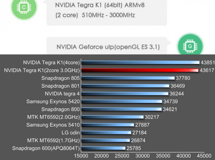 000 MHz 000 MHz |
350 MHz | ||||||
| GPU boost clock | 1.000 MHz | 1150 MHz | ||||||
| GPU FP32 floating point | 512 GFLOPS | 384 GFLOPS | ||||||
| Socket | SoC | LGA1151 | ||||||
| Compatible motherboard | — | Socket LGA 1151 Motherboard | ||||||
| (Android 64-bit | Linux 64-bit) Geekbench 4 single core |
1.158 | 5.887 | ||||||
| (Android 64-bit | Linux 64-bit) Geekbench 4 multi-core |
3.276 | 16.660 | ||||||
| (SGEMM) GFLOPS performance |
33,6 GFLOPS | 326,1 GFLOPS | ||||||
| (Multi-core / watt performance) Performance / watt ratio |
218 pts / W | 183 pts / W | ||||||
| Amazon | ||||||||
| eBay |
Note: Commissions may be earned from the links above.
We can better compare what are the technical differences between the two processors.
Suggested PSU: We assume that we have An ATX computer case, a high end graphics card, 16GB RAM, a 512GB SSD, a 1TB HDD hard drive, a Blu-Ray drive. We will have to rely on a more powerful power supply if we want to have several graphics cards, several monitors, more memory, etc.
Price: For technical reasons, we cannot currently display a price less than 24 hours, or a real-time price. This is why we prefer for the moment not to show a price. You should refer to the respective online stores for the latest price, as well as availability.
The processor Nvidia Tegra X1 T210 has more cores, the turbo frequency of Intel Core i7-7700K is bigger, that the PDT of Nvidia Tegra X1 T210 is lower. The Intel Core i7-7700K was started more recently.
Performances :
Performance comparison between the two processors, for this we consider the results generated on benchmark software such as Geekbench 4.
| Geekbench 4 — Multi-core & single core score — Linux & Android 64-bit | |
|---|---|
| Intel Core i7-7700K |
5.887 16.660 |
| Nvidia Tegra X1 T210 |
1.158 3.276 |
In single core, the difference is 408%. In multi-core, the difference in terms of gap is 409%.
Note: Commissions may be earned from the links above. These scores are only an
average of the performances got with these processors, you may get different results.
Geekbench 4 is a complete benchmark platform with several types of tests, including data compression, images, AES encryption, SQL encoding, HTML, PDF file rendering, matrix computation, Fast Fourier Transform, 3D object simulation, photo editing, memory testing. This allows us to better visualize the respective power of these devices. For each result, we took an average of 250 values on the famous benchmark software.
Equivalence:
Nvidia Tegra X1 T210 Intel equivalentNvidia Tegra X1 T210 AMD equivalentIntel Core i7-7700K AMD equivalent
See also:
Intel Core i7-7700Intel Core i7-7700HQIntel Core i7-7700T
Tesla MCU Index — ARM Tegra, Intel Atom, AMD Ryzen
Welcome to Tesla Motors Club
Discuss Tesla’s Model S, Model 3, Model X, Model Y, Cybertruck, Roadster and More.
Register
JavaScript is disabled. For a better experience, please enable JavaScript in your browser before proceeding.
#1
-
-
#1
A comparative index of the differences between MCU1, MCU2 and MCU3/MCUZ. ..
..
Sources and related threads:
AMD Ryzan speed comparison vs Intel Atom
https://teslamotorsclub.com/tmc/threads/new-model-y-performance-no-ryzen.258552/
https://insideevs.com/news/561232/amd-ryzen-affects-range-tesla/
https://teslanorth.com/2021/11/30/tesla-model-y-amd-ryzen-vs-model-3-with-intel-atom-chip-video/
https://teslatap.com/articles/autopilot-processors-and-hardware-mcu-hw-demystified/
https://videocardz.com/newz/tesla-c…n-ryzen-embedded-apu-and-discrete-navi-23-gpu
https://wccftech.com/amds-ryzen-cpu-reportedly-cuts-down-tesla-model-3s-driving-range/
https://www.cpu-world.com/Compare/231/Intel_Atom_x5_Z8350_vs_Intel_Atom_x7_E3950.html
https://www.intel.com/content/www/u…r-2m-cache-up-to-2-00-ghz/specifications.html
Last edited:
Reactions:
scottf200, t3sl4drvr and whatthe2
#2
-
-
#2
To me the largest advantage of MCU3 over MCU2 seems to be that Tesla is more likely continues to supporting MCU3 for longer than they will support MCU2. This would include new software releases including features for MCU2, protecting software against regressions specific only to MCU2, keeping the software releases performing well on MCU2, and releasing any software updates at all to MCU2.
Tesla already has practically stopped supporting MCU1 that was still in new cars sold just four years ago. Today all those cars are out-of-warranty and Tesla does not seem to have any obligation of keeping those cars working properly. When exactly we can expect MCU2 support to become similar disaster compared to MCU1 is unknown. My guess would be 2026, when the last MCU2 cars are out-of-warranty.
I hope regulators will force manufacturers to commit to clear timelines when selling a car. Purchasing a new car today leaves it unclear how well — if at all a properly maintained car will work — in 10 years from the purchase date.
#3
-
-
#3
I wish Tesla will make MCU3 upgrade available to MCU1 cars. That would give those cars a way longer life extension compared to an already out-of-date MCU2 upgrade.
#4
-
-
#4
Can one upgrade from MCU2 to MCU3?
#5
-
-
#5
TMYB-C1 said:
Can one upgrade from MCU2 to MCU3?
Click to expand.
..
Still waiting for the first person to try on the S/X. Getting the UI to run vertically on it may be harder that faking the liquid cooling. Also tricky that MCU3 has HWx integrated.
The 3/Y ought to be easier since none of those three problems exist, but Green says it still won’t happen mostly due to physical size and harness/power.
Size and power should come down in a theoretical MCU4, so maybe later.
Last edited:
#6
-
-
#6
TMYB-C1 said:
Can one upgrade from MCU2 to MCU3?
Click to expand.
..
Not currently, and likely not ever although a small possibility on the 3/Y. On the S/X there is nothing similar between MCU2 and MCU3 as far as wiring, connectors, placement, and more. MCU3 required liquid cooling, which is not available in the cabin for cars made for MCU1 or MCU2 with the S/X. Now for the 3/Y, there is perhaps some hope as MCU2 was water cooled and the physical placement hasn’t changed. I don’t know if the connectors changed or if other key electrical changes were made in the 3/Y when Tesla switched from MCU2 to MCU3 which would prevent a reasonable retrofit.
#7
-
-
#7
I just had my MCU/whole touch screen replaced this week on our 2020 LR+ Model X. They have to address a few other things, but when I played with the touchscreen and map rendering, it was noticeably faster than the original MCU that came with the car (something I observed on delivery). The units are clearly MCU2, but curious if there are variations of MCU2 if MCU3 may not be supported on vertical screen S/X’s?
#8
-
-
#8
EV bud said:
…curious if there are variations of MCU2…
Click to expand.
..
Interesting question. I’m sure there are minor revisions, but I suspect the specifications are identical.
Obviously you can’t put a Ryzen on an Atom board, but it would be interesting to see if the chipset that the MCU2 board uses supports any other CPUs. I assume some here are good enough to float a new BGA CPU on a rework station.
Reactions:
Droschke
#9
-
-
#9
I suspect they have a couple suppliers for certain chipsets and some just don’t perform as well as others, but are «within spec». Have there been any known warranty replacements on vertical S/X vehicles with MCU3?
#10
-
-
#10
Krash said:
Interesting question. I’m sure there are minor revisions, but I suspect the specifications are identical.
Click to expand…
Wouldn’t the part numbers be different then?
#11
-
-
#11
Droschke said:
Wouldn’t the part numbers be different then?
Click to expand.
..
I’m pretty sure there is only one part number.
Last edited:
Reactions:
Droschke
#12
-
-
#12
Anyone ever determine if the MCU3 modem is 5G capable?
#13
-
-
#13
Looks like there may be a new part number for the MCU2? Unfortunately, the replacement didn’t fix my issue. Screen stills freezes, more debugging needed.
Reactions:
Krash
#14
-
-
#14
Thanks for this @Krash. Is there any other source of model numbers? I’d like to search for a MCU3 on ebay, but 1637790 only brings up MCU-Z. And for instance when I search on ebay and look at pics, I can see lots of other model numbers like 1775000 or 1684435 or 1681271 which aren’t listed in that table, and ideally I’d like to create a saved ebay search for a known-correct part number. (It’s hard to see but I think the 1684435 is the part number of this one which is claimed to be an MCU3 one?)
#15
-
-
#15
Anyone else notice that T-Mobile is licensing part of its spectrum to Starlink so that it’s customers can use Starlink v2 satellite data in the future? Some debate about whether the spectrum is 5G or older PCS.
Hmmm.
5G in MCU3/MCUZ (speculated) plus a switch from AT&T to T-Mobile would mean instant Starlink in the future. Somebody at Tesla has to be thinking about this.
Last edited:
Tesla lowers Model 3 range estimates in Europe due to extra power consumption of AMD Ryzen processor
- whiskeylover
- Model 3
2
3
4
- Replies
- 74
- Views
- 7K
Model 3
eSzeL
Model S refresh infotainment system powered by AMD’s NAVI 23
- mlkmade
- Model S
- Replies
- 6
- Views
- 1K
Model S
Krash
Powered by Primary
Share:
Facebook
Twitter
Reddit
Pinterest
Tumblr
WhatsApp
Email
Share
Link
Forum list
Intel Core i5-7600K vs Nvidia Tegra 3 T33 Comparison
VS
Intel Core i5-7600K
Buy on Amazon
Nvidia Tegra 3 T33
Buy on Amazon
- Key Differences
- Performance
- Features
- Miscellaneous
- General info
- Memory
- Benchmarks
Intel Core i5-7600K
Nvidia Tegra 3 T33
| Cores | 4 | 4 |
| CPU Threads | 4 | 4 |
| Base Clock Speed | 3. 8GHz 8GHz |
1.6GHz |
| Turbo Clock Speed | 4.2GHz | Not Known |
| TDP (THERMAL DESIGN POINT) | 91W | Not Known |
| Has integrated graphics | Yes | Yes |
| Performance per watt | Not Known | Not Known |
| CPU Speed & Cores | 4 x 3. 8GHz 8GHz |
4 x 1.6GHz |
| Number of CPU Threads | 4 | 4 |
| L2 Cache Size | 1MB | 1MB |
| L3 Cache Size | 6MB | Not Known |
| Turbo Boost Frequency | 4. 2GHz 2GHz |
Not Known |
| L1 Cache Size | 256KB | 256KB |
| L2 Core | 0. 25MB/core 25MB/core |
0.25MB/core |
| L3 Core | 1. 5MB/core 5MB/core |
Not Known |
| Clock Multiplier | 38 | Not Known |
| Turbo Boost Tech Version | 2 | Not Known |
| Does it have an unlocked multiplier | No | No |
Uses ARM big. LITTLE tech LITTLE tech |
No | No |
| Uses ARM HMP | No | No |
| Has AES Support | Yes | No |
| Supports CPU Throttling | Yes | Yes |
| Supported SSE Version | 4. 2 2 |
Not Known |
| Has AVX Support | Yes | No |
| Has MMX Tech Support | Yes | No |
| Has F16C Support | Yes | No |
No. of Bits Executed at a Time of Bits Executed at a Time |
Not Known | 64 |
| CPU Front-End Width | Not Known | 2 |
| Supports ARM TrustZone Tech | No | Yes |
| Has FMA4 Instructions Support | No | No |
| Has Multithreading Tech Support | No | No |
| VFP Version | Not Known | 3 |
| Has NX Processor Bit Support | Yes | Yes |
| Has FMA3 Instructions Support | Yes | No |
| Width Size | 37. 5mm 5mm |
14mm |
| Height | 37. |
14mm |
| RAM Memory Speed | 2400MHz | 800MHz |
| Max Memory Bandwidth | 38. |
6.4GB/s |
| Max Memory Channels | 2 | 1 |
| Supported Memory Size | 64GB | 2GB |
| Bus Bandwidth | 8GT/s | Not Known |
| ECC (Error-Correcting Code) Memory Support | No | No |
| PassMark Score | 9277 | Not Known |
| PassMark Score (Single Thread) | 2396 | Not Known |
Similar Comparisons
0025 667MHz higher RAM speed?
1600MHz vs 933MHz
22nm vs 28nm
16GB vs 4GB
Why is Nvidia Tegra 4 better than Intel Core i5-4200U?
- 2.
37x higher CPU speed?
4 x 1.9GHz vs 2 x 1.6GHz - GPU frequency 472MHz higher?
672MHz vs 200MHz - 1.5MB more L2 cache?
2MB vs 0.5MB - 128KB more L1 cache?
256KB vs 128KB - 0.25MB/core more L2 cache per core?
0.5MB/core vs 0.25MB/core - Has TrustZone?
What are the most popular comparisons?
Intel Core i5-4200u
VS
Intel Celeron N3060
NVIDIA TEGRA 4
VS
NVIDIA TEGRA K1 (64-bit)
9000 VS 9000 AMD 9000 AMD AMD
Nvidia Tegra 4
vs
Qualcomm Snapdragon 888
Intel Core i5-4200U
vs
Intel Core i3-7100
Nvidia Tegra 4
vs
Qualcomm Snapdragon 865 Plus
Intel Core i5-4200U
vs
AMD A6-5350M
Nvidia Tegra 4
vs
Nvidia Tegra 3 T33
Intel Core i5-4200U
vs
Intel Celeron N3350
Nvidia Tegra 4
vs
Nvidia Tegra K1 (32-bit)
Intel Core i5-4200u
VS
A8-55503
NVIDIA TEGRA 4
VS
ARM Cortex-A53
Intel Core i5-4200U
VS 9000 9000 9000 i5-1135G7
Nvidia Tegra 4
vs
Qualcomm Snapdragon 835
Intel Core i5-4200U
vs
AMD A10-5750M
Nvidia Tegra 4
vs
Nvidia Tegra 4i
Intel Core i5-4200U
VS
Intel Celeron N4020
NVIDIA TEGRA 4
VS
Qualcomm Snapdragon S4 PRO MSM89603
Intel Core I5-4200U
VS
Intel Pentel Pentel Pentel Pentel Pentel Pentel Pentel Pentel Pentel Pentel Pentel Pentel Pentel Pentel Pentel Pentel Pentel Pentel Pentel Pentel0003
VS
Apple A14 Bionic
Comers execute a processor considering all its cores (processors).
It is calculated by adding the clock speeds of each core or, in the case of multi-core processors, each group of cores.
2nd processor thread
More threads result in better performance and better multitasking.
3.speed turbo clock
2.6GHz
Unknown. Help us offer a price. (Nvidia Tegra 4)
When the processor is running below its limits, it can jump to a higher clock speed to increase performance.
4. Has an unlocked multiplier of
✖Intel Core i5-4200U
✖Nvidia Tegra 4
Some processors come with an unlocked multiplier and are easier to overclock, allowing you to get better quality in games and other applications.
5.L2 Cache
More L2 scratchpad memory results in faster results in CPU and system performance tuning.
6.L3 cache
Unknown. Help us offer a price. (Nvidia Tegra 4)
More L3 scratchpad results in faster results in CPU and system performance tuning.
7.L1 cache
More L1 cache results in faster results in CPU and system performance tuning.
8.core L2
0.25MB/core
0.5MB/core
More data can be stored in the L2 scratchpad for access by each processor core.
9.core L3
1.5MB/core
Unknown. Help us offer a price. (Nvidia Tegra 4)
More data can be stored in L3 scratchpad for access by each processor core.
Memory
1.RAM speed
1600MHz
933MHz
Can support faster memory which speeds up system performance.
2.max memory bandwidth
25.6GB/s
Unknown. Help us offer a price. (Nvidia Tegra 4)
This is the maximum rate at which data can be read from or stored in memory.
3rd DDR memory version
Unknown. Help us offer a price. (Nvidia Tegra 4)
DDR (Dynamic Dynamic Random Access Memory Double Data Rate) is the most common type of main memory. New versions of DDR memory support higher maximum speeds and are more energy efficient.
4.Memory channels
More memory channels increase the speed of data transfer between memory and processor.
5.Maximum memory
Maximum memory (RAM).
6.bus baud rate
Unknown. Help us offer a price. (Intel Core i5-4200U)
Unknown. Help us offer a price. (Nvidia Tegra 4)
The bus is responsible for transferring data between various components of a computer or device.
7. Supports memory troubleshooting code
✖Intel Core i5-4200U
✖Nvidia Tegra 4
Memory troubleshooting code can detect and fix data corruption. It is used when necessary to avoid distortion, such as in scientific computing or when starting a server.
8.eMMC version
Unknown. Help us offer a price. (Intel Core i5-4200U)
Unknown. Help us offer a price. (Nvidia Tegra 4)
A newer version of eMMC — built-in flash memory card — speeds up the memory interface, has a positive effect on device performance, for example, when transferring files from a computer to internal memory via USB.
9.bus frequency
Unknown. Help us offer a price. (Intel Core i5-4200U)
Unknown. Help us offer a price. (Nvidia Tegra 4)
The bus is responsible for transferring data between various components of a computer or device
Geotagging
1. PassMark result
Unknown. Help us offer a price. (Nvidia Tegra 4)
This benchmark measures CPU performance using multithreading.
2nd PassMark result (single)
Unknown. Help us offer a price. (Nvidia Tegra 4)
This benchmark measures processor performance using a thread of execution.
3.Geekbench 5 result (multi-core)
Unknown. Help us offer a price. (Nvidia Tegra 4)
Geekbench 5 is a cross-platform benchmark that measures multi-core processor performance. (Source: Primate Labs, 2022)
4. Cinebench R20 result (multi-core)
Unknown. Help us offer a price. (Nvidia Tegra 4)
Cinebench R20 is a benchmark that measures the performance of a multi-core processor by rendering a 3D scene.
5.Cinebench R20 result (single core)
Unknown. Help us offer a price. (Nvidia Tegra 4)
Cinebench R20 is a test to evaluate the performance of a single core processor when rendering a 3D scene.
6.Geekbench 5 result (single core)
Unknown. Help us offer a price. (Nvidia Tegra 4)
Geekbench 5 is a cross-platform benchmark that measures the single-core performance of a processor. (Source: Primate Labs, 2022)
7. Blender test result (bmw27)
Unknown. Help us offer a price. (Intel Core i5-4200U)
Unknown. Help us offer a price. (Nvidia Tegra 4)
The Blender benchmark (bmw27) measures CPU performance by rendering a 3D scene. More powerful processors can render a scene in a shorter time.
8.Blender result (classroom)
Unknown. Help us offer a price. (Intel Core i5-4200U)
Unknown. Help us offer a price. (Nvidia Tegra 4)
The Blender (classroom) test measures CPU performance by rendering a 3D scene. More powerful processors can render a scene in a shorter time.
9.power per watt
Unknown. Help us offer a price. (Intel Core i5-4200U)
Unknown. Help us offer a price. (Nvidia Tegra 4)
This means that the processor is more efficient, giving more performance per watt of power used.
Functions
1.uses multithreading
✔Intel Core i5-4200U
✖Nvidia Tegra 4
processor into logical cores, also known as threads. Thus, each core can run two instruction streams at the same time.
2. Has AES
✔Intel Core i5-4200U
✖Nvidia Tegra 4
AES is used to speed up encryption and decryption.
3. Has AVX
✔Intel Core i5-4200U
✖Nvidia Tegra 4
AVX is used to help speed up calculations in multimedia, scientific and financial applications, and to improve the performance of the Linux RAID program.
SSE 4th version
Unknown. Help us offer a price. (Nvidia Tegra 4)
SSE is used to speed up multimedia tasks such as editing images or adjusting audio volume. Each new version contains new instructions and improvements.
5.Has F16C
✔Intel Core i5-4200U
✖Nvidia Tegra 4
F16C is used to speed up tasks such as image contrast adjustment or volume control.
6.bits transmitted at the same time
Unknown. Help us offer a price. (Intel Core i5-4200U)
128 (ARM Cortex-A15)
NEON provides faster media processing such as MP3 listening.
7. Has MMX
✔Intel Core i5-4200U
✖Nvidia Tegra 4
MMX is used to speed up tasks such as adjusting image contrast or adjusting volume.
8.Has TrustZone
✖Intel Core i5-4200U
✔Nvidia Tegra 4 (ARM Cortex-A15)
Technology is integrated into the processor to ensure device security when using features such as mobile payments and streaming video using technology digital rights management (DRM).
9.interface width
Unknown. Help us offer a price. (Intel Core i5-4200U)
3 (ARM Cortex-A15)
The processor can decode more instructions per clock (IPC), which means that the processor performs better
Price comparison
Cancel
Which CPU is better?
This page is currently only available in English.
Intel Core i5-4300U vs Nvidia Tegra 3 T30: What is the difference?
38 points
Intel Core i5-4300U
26 BALLLA
NVIDIA TEGRA 3 T30
Winter when comparing
VS
67 Facts compared to
Intel Core i5-4300U
NVIDIA TEGRA 3 T30
Why I5-4300U is better than NVIDIA TEGRA ?
- Supports 64-bit system?
- 850MHz higher RAM speed?
1600MHz vs 750MHz - Semiconductor size 18nm smaller?
22nm vs 40nm - 19.
6GB/s more memory bandwidth?
25.6GB/s vs 6GB/s - 14GB more max memory?
16GB vs 2GB - 1 more memory channels?
2 vs 1 - Has AES?
- Uses multithreading?
Why is Nvidia Tegra 3 T30 better than Intel Core i5-4300U?
- 47.37% higher CPU speed?
4 x 1.4GHz vs 2 x 1.9GHz - GPU frequency 320MHz higher?
520MHz vs 200MHz - 0.5MB more L2 cache?
1MB vs 0.5MB - 192KB more L1 cache?
256KB vs 64KB - Has TrustZone?
What are the most popular comparisons?
Intel Core i5-4300U
vs
Intel Celeron N5100
Nvidia Tegra 3 T30
vs
MediaTek Helio G35
Intel Core i5-4300U
vs
Intel Core i3-1115G4
Nvidia Tegra 3 T30
vs
Nvidia Tegra 3 T33
Intel Core i5-4300U
vs
AMD A10-8700P
NVIDIA TEGRA 3 T30
VS
NVIDIA TEGRA K1 (64-bit)
Intel Core i5-4300U
VS
Intel Atom X7-Z8700
NVIDIA TEGRA vs.
Qualcomm Snapdragon 600 APQ8064T
Intel Core i5-4300U
vs
AMD Ryzen 3 4300U
Nvidia Tegra 3 T30
vs
Qualcomm Snapdragon S4 Plus MSM8960
Intel Core i5-4300U
vs
Intel Core i5-3427u
NVIDIA TEGRA 3 T30
VS
NVIDIA TEGRA K1 (32-bit)
Intel Core i5-4300U
VS
Intel Core i5-8250U
NVIDIA TEGRA TEGRA TEGRA0003
VS
MediaTek MT6582
Intel Core i5-4300U
VS
AMD PRO A8-8600B
Intel Core i5-4300U
VS
I5-6300U
22222 vs
Intel Core i5-7Y57
Comparison of prices
Users reviews
General rating
Intel Core i5-4300U
1 Reviews of Users
Intel Core i5-4300u
04 /10
1 reviews of users
NVIDIA TEGRA 3 t3 /10
1 Votes
reviews not yet
Games
10.0 /10
1 Votes
reviews yet there is no
9000 9000
002 performance
10. 0 /10
1 Votes
Reviews yet not
Reliability
6.0705 /10
1 VOTES
Reviews yet not
Energy
905 8.0 10
1 votes
No reviews yet
Performance
1.cpu speed
2 x 1.9GHz
4 x 1.4GHz
CPU speed indicates how many processing cycles per second the processor can perform, considering all its cores (processors). It is calculated by adding the clock speeds of each core or, in the case of multi-core processors, each group of cores.
2nd processor thread
More threads result in better performance and better multitasking.
3.speed turbo clock
2.9GHz
Unknown. Help us offer a price. (Nvidia Tegra 3 T30)
When the processor is running below its limits, it can jump to a higher clock speed to increase performance.
4. Unlocked
✖Intel Core i5-4300U
✖Nvidia Tegra 3 T30
Some processors come with an unlocked multiplier and are easier to overclock, allowing for better performance in games and other applications.
5.L2 cache
More L2 scratchpad memory results in faster results in CPU and system performance tuning.
6.L3 cache
Unknown. Help us offer a price. (Nvidia Tegra 3 T30)
More L3 scratchpad memory results in faster results in CPU and system performance tuning.
7.L1 cache
More L1 cache results in faster results in CPU and system performance tuning.
8.core L2
0.25MB/core
0.25MB/core
More data can be stored in the L2 scratchpad for access by each processor core.
9.core L3
1.5MB/core
Unknown. Help us offer a price. (Nvidia Tegra 3 T30)
More data can be stored in L3 scratchpad for access by each processor core.
Memory
1st RAM speed
1600MHz
750MHz
Can support faster memory which speeds up system performance.
2.max memory bandwidth
25.6GB/s
This is the maximum rate at which data can be read from or stored in memory.
3rd DDR memory version
Unknown. Help us offer a price. (Nvidia Tegra 3 T30)
DDR (Double Data Rate Synchronous Dynamic Random Access Memory) is the most common type of RAM. New versions of DDR memory support higher maximum speeds and are more energy efficient.
4.Memory channels
More memory channels increase the speed of data transfer between memory and processor.
5.Maximum memory
Maximum memory (RAM).
6.bus baud rate
Unknown. Help us offer a price. (Nvidia Tegra 3 T30)
The bus is responsible for transferring data between various components of a computer or device.
7.Supports memory troubleshooting code
✖Intel Core i5-4300U
✖Nvidia Tegra 3 T30
The memory error recovery code can detect and repair data corruption. It is used when necessary to avoid distortion, such as in scientific computing or when starting a server.
8.eMMC version
Unknown. Help us offer a price. (Intel Core i5-4300U)
Unknown. Help us offer a price. (Nvidia Tegra 3 T30)
A newer version of eMMC — built-in flash memory card — speeds up the memory interface, has a positive effect on device performance, for example, when transferring files from a computer to internal memory via USB.
9.bus frequency
Unknown. Help us offer a price. (Intel Core i5-4300U)
Unknown. Help us offer a price. (Nvidia Tegra 3 T30)
The bus is responsible for transferring data between various components of a computer or device
Geotagging
1. PassMark result
Unknown. Help us offer a price. (Nvidia Tegra 3 T30)
This benchmark measures CPU performance using multithreading.
2nd PassMark result (single)
Unknown. Help us offer a price. (Nvidia Tegra 3 T30)
This benchmark measures processor performance using a thread of execution.
3.Geekbench 5 result (multi-core)
Unknown. Help us offer a price. (Nvidia Tegra 3 T30)
Geekbench 5 is a cross-platform benchmark that measures multi-core processor performance. (Source: Primate Labs, 2022)
4.Cinebench R20 result (multi-core)
Unknown. Help us offer a price. (Nvidia Tegra 3 T30)
Cinebench R20 is a benchmark that measures the performance of a multi-core processor by rendering a 3D scene.
5.Cinebench R20 result (single core)
Unknown. Help us offer a price. (Nvidia Tegra 3 T30)
Cinebench R20 is a test to evaluate the performance of a single core processor when rendering a 3D scene.
6.Geekbench 5 result (single core)
Unknown. Help us offer a price. (Nvidia Tegra 3 T30)
Geekbench 5 is a cross-platform benchmark that measures the single-core performance of a processor. (Source: Primate Labs, 2022)
7. Blender test result (bmw27)
1689.5seconds
Unknown. Help us offer a price. (Nvidia Tegra 3 T30)
The Blender benchmark (bmw27) measures CPU performance by rendering a 3D scene. More powerful processors can render a scene in a shorter time.
8. Blender result (classroom)
Unknown. Help us offer a price. (Intel Core i5-4300U)
Unknown. Help us offer a price. (Nvidia Tegra 3 T30)
The Blender (classroom) benchmark measures CPU performance by rendering a 3D scene. More powerful processors can render a scene in a shorter time.
9.power per watt
Unknown. Help us offer a price. (Intel Core i5-4300U)
Unknown. Help us offer a price. (Nvidia Tegra 3 T30)
This means the processor is more efficient, giving more performance per watt of power used.
Functions
1.uses multithreading
✔Intel Core i5-4300U
✖Nvidia Tegra 3 T30
processor cores into logical cores, also known as threads. Thus, each core can run two instruction streams at the same time.
2. Has AES
✔Intel Core i5-4300U
✖Nvidia Tegra 3 T30
AES is used to speed up encryption and decryption.
3. Has AVX
✔Intel Core i5-4300U
✖Nvidia Tegra 3 T30
AVX is used to help speed up calculations in multimedia, scientific and financial applications, and to improve the performance of the Linux RAID program.
SSE 4th version
Unknown. Help us offer a price. (Nvidia Tegra 3 T30)
SSE is used to speed up multimedia tasks such as editing images or adjusting audio volume. Each new version contains new instructions and improvements.
5.Has F16C
✔Intel Core i5-4300U
✖Nvidia Tegra 3 T30
F16C is used to speed up tasks such as image contrast adjustment or volume control.
6.bits transmitted at the same time
Unknown. Help us offer a price. (Intel Core i5-4300U)
NEON provides faster media processing such as MP3 listening.
7. Has MMX
✔Intel Core i5-4300U
✖Nvidia Tegra 3 T30
MMX is used to speed up tasks such as adjusting image contrast or adjusting volume.
8. Has TrustZone
✖Intel Core i5-4300U
✔Nvidia Tegra 3 T30
Technology is integrated into the processor to ensure device security when using features such as mobile payments and streaming video using Digital Rights Management (DRM) technology ).
9.interface width
Unknown. Help us offer a price. (Intel Core i5-4300U)
The processor can decode more instructions per clock (IPC), which means that the processor performs better
Other
1.OpenGL ES version
Unknown. Help us offer a price. (Intel Core i5-4300U)
OpenGL ES is used to play on mobile devices such as smartphones. Later versions support better graphics.
OpenVG version 2
Unknown. Help us offer a price. (Intel Core i5-4300U)
OpenVG is used to improve 2D graphics on mobile devices, such as the user interface (UI) on a smartphone.
3. EGL version
Unknown. Help us offer a price. (Intel Core i5-4300U)
EGL is used on smartphones to make OpenVG and OpenGL ES work better.
Price comparison
Cancel
Which CPU is better?
Intel UHD Graphics (Jasper Lake 16 EU) vs Tegra X1.
VS
General Information
The general information section of the video card comparison list provides release date, type, overall rating and other useful data to determine the winner between Intel UHD Graphics (Jasper Lake 16 EU) and Tegra x1. Please note that the comparison takes place on all indicators, and below are the ratings from synthetic benchmarks that define different criteria in games and work applications.
701
Performance Rating Position
not rated
Gen. 11
Architecture
Maxwell 2.0
11 January 2021 (Less than a Year AGO)
Release date
No Data
No data
Actual price
$ 239
Gen. 11
GPU Code Name
GM20B
Laptop
Market Segment
Desktop
Specifications
Which graphics card is better in Intel UHD Graphics (Jasper Lake 16 EU) vs Tegra X1 comparison in manufacturing process, power consumption, and base and turbo frequency of the GPU is the most important part contained in the rating of graphics cards.
350 MHZ
Tibility of the nucleus
1000 MHZ
10 NM
Technological process
20 NM
No data
Texles processed in 1 second
16.00
24
Converse / CUDA Nuclei
256
800 MHZ
Acceleration speed
No data
Number of transistors
2.000 Million
No data Country Cleaner power
15 Watt
Dimensions, connectors and compatibility
Let’s discuss the dimensions (length, width, height) of Intel UHD Graphics (Jasper Lake 16 EU) and Tegra X1 graphics cards. As well as the main types of connectors and connected interfaces
N/A
Interface
IGP
Memory (frequency and overclocking)
Graphics card memory plays an important role in both gaming and graphics applications. The higher the standard ( GDDR ), the better. It directly affects the speed and efficiency of data processing. What is the difference in type, base and turbo frequency, GDDR bandwidth between Intel UHD Graphics (Jasper Lake 16 EU) and Tegra X1:
N/A
Memory type
System Shared
Port and display support
Let’s find out the difference in ports that Intel UHD Graphics (Jasper Lake 16 EU) and Tegra X1 are equipped with. Pay attention to the number of ports and the maximum resolution of supported monitors.
No data
Display connections
No outputs
Technologies
Let’s see what the difference is. It is worth noting that NVIDIA and AMD use different technologies.
+
Quick Sync
No data
API support
The confrontation between the two rivals Intel UHD Graphics (Jasper Lake 16 EU) and Tegra X1 is almost over. Hardware support (API) does not greatly affect the overall performance, it is not taken into account in synthetic benchmarks and other performance tests.
n.a.
DirectX
12 (12_1)
n.a.
OpenGL
4.6
Intel UHD Graphics (Jasper Lake 16 EU) versus Tegra X1 benchmark comparison
Popular comparisons with selected graphics cards
| one. | Intel Iris Xe Graphics G7 vs. Intel UHD Graphics (Jasper Lake 16 EU) | |
|
2. |
Intel UHD Graphics (Jasper Lake 16 EU) vs. GeForce G 102M | |
| 3. | Intel UHD Graphics (Jasper Lake 16 EU) vs. NV18 A4 | |
| four. |
Intel UHD Graphics (Jasper Lake 16 EU) vs. |
|
| 5. | Intel UHD Graphics (Jasper Lake 16 EU) vs. NV17 A5 | |
| 6. | Intel UHD Graphics (Jasper Lake 16 EU) vs. GeForce4 MX 440 Mac Edition | |
| 7. |
Intel UHD Graphics (Jasper Lake 16 EU) vs. |
|
| eight. | Intel UHD Graphics (Jasper Lake 16 EU) vs. Tesla V100 DGXS | |
| 9. | Intel UHD Graphics (Jasper Lake 16 EU) vs. Intel UHD Graphics 630 | |
| ten. |
Intel Iris Xe MAX Graphics vs. |
|
| eleven. | Intel UHD Graphics (Jasper Lake 16 EU) vs. NV15 A5 | |
| 12. | Intel UHD Graphics (Jasper Lake 16 EU) vs. TU104 | |
| 13. |
Intel UHD Graphics (Jasper Lake 16 EU) vs. |
|
| fourteen. | Intel UHD Graphics (Jasper Lake 16 EU) vs. GeForce 8400GS Rev. 2 | |
| fifteen. | Intel UHD Graphics (Jasper Lake 16 EU) vs. XGI XG40 |
Comparison of Intel UHD Graphics 750 and NVIDIA Tegra 3
Comparative analysis of Intel UHD Graphics 750 and NVIDIA Tegra 3 video cards by all known characteristics in the categories: General information, Specifications, Video outputs and ports, API support, Compatibility, dimensions, requirements.
Analysis of video card performance by benchmarks: PassMark — G3D Mark, PassMark — G2D Mark, Geekbench — OpenCL, GFXBench 4.0 — Car Chase Offscreen (Frames), GFXBench 4.0 — Manhattan (Frames), GFXBench 4.0 — T-Rex (Frames), GFXBench 4.0 — Car Chase Offscreen (Fps), GFXBench 4.0 — Manhattan (Fps), GFXBench 4.0 — T-Rex (Fps), 3DMark Fire Strike — Graphics Score.
Intel UHD Graphics 750
versus
NVIDIA Tegra 3
Benefits
Reasons to choose Intel UHD Graphics 750
- The video card is newer, the difference in release dates is 10 year(s) 10 month(s)
- times a) more: 1300 MHz vs 520 MHz
- A newer manufacturing process for the video card allows it to be more powerful, but with lower power consumption: 14 nm vs 40 nm
- Approximately 33% less power consumption: 15 Watt vs 20 Watt
| Release date | 2021 vs 9 November 2011 |
| Boost core clock | 1300 MHz vs 520 MHz |
| Process | 14 nm vs 40 nm |
| Power Demand (TDP) | 15 Watt vs 20 Watt |
Reasons to choose NVIDIA Tegra 3
- About 39% more core clock: 416 MHz vs 300 MHz
| Core clock | 416 MHz vs 300 MHz |
Benchmark comparison
GPU 1: Intel UHD Graphics 750
GPU 2: NVIDIA Tegra 3
| Name | Intel UHD Graphics 750 | NVIDIA Tegra 3 |
|---|---|---|
| PassMark — G3D Mark | 1752 | |
| PassMark — G2D Mark | 341 | |
| Geekbench — OpenCL | 7782 | |
| GFXBench 4. |
2899 | |
| GFXBench 4.0 — Manhattan (Frames) | 3219 | |
| GFXBench 4.0 — T-Rex (Frames) | 11068 | |
| GFXBench 4.0 — Car Chase Offscreen (Fps) | 2899 | |
| GFXBench 4.0 — Manhattan (Fps) | 3219 | |
| GFXBench 4.0 — T-Rex (Fps) | 11068 | |
| 3DMark Fire Strike — Graphics Score | 656 |
Feature comparison
| Intel UHD Graphics 750 | NVIDIA Tegra 3 | |
|---|---|---|
| Architecture | Generation 12. |
GeForce ULP |
| Codename | Rocket Lake GT1 | Tegra 3 |
| Issue date | 2021 | November 9, 2011 |
| Place in the rating | 551 | not rated |
| Type | Desktop | Desktop |
| Boost 9 core clock1216 | 1300 MHz | 520MHz |
| Number of Compute | 32 | |
| Core frequency | 300MHz | 416 MHz |
| Process | 14nm | 40nm |
| Peak Double Precision (FP64) Performance | 166. |
|
| Peak Half Precision (FP16) Performance | 1331 GFLOPS (2:1) | |
| Peak Single Precision (FP32) Performance | 665.6GFLOPS | |
| Number of shaders | 256 | |
| Pixel fill rate | 10.40 GPixel/s | |
| Texturing speed | 20.80 GTexel/s | |
| Power consumption (TDP) | 15 Watt | 20 Watt |
| Number of transistors | 10 million | |
| Video connectors | No outputs | No outputs |
| DirectX | 12. |
N/A |
| OpenCL | 3.0 | |
| OpenGL | 4.6 | ES 2.0 |
| Shader Model | 6.4 | |
| Vulcan | ||
| Interface | IGP |
Repair your Tesla yourself, you programmer / Sudo Null IT News
You programmer, honor and praise to you. You may have spent your youth in a stretchy wool sweater, but now you proudly laugh in the face of any joke about IT people. Perhaps the time has passed for repairing cars with internal combustion engines with men in garages, but . … Valera, your time has come.
You are an IT specialist, women look at you with adoration and men with envy. It’s good that you are already at the computer, we will hack Tesla with two keyboards.
First you need to understand the hardware in your Tesla. We are interested in MCU (Media Control Unit), MCU1 (Tegra) and MCU2 (Intel) happen.
Tesla has a special diagnostic mode that shows all current errors, 100 latest errors. It is possible to open the service menu to calibrate individual nodes.
If you have pre-styling Tesla model S on MCU1. We connect instead of the dashboard to Fakro-Lan and run the translation script in the factory. Factory mode differs from Developer mode in that it doesn’t crash after a reboot.
 #!/bin/bash
#
# Put Tesla MCU1 in factory mode
#
# Call over diagnostics port with seceth enabled
#
# Reboot MCU later
#
VALUE=true
if[! -z "$1" ]; then
    VALUE=$1
fi
CID="192.168.90.100"
curl "http://${CID}:4070/_data_set_value_request_?name=GUI_factoryMode&value=${VALUE}"
To receive updates and control the car through the app, you need live certificates on the machine. Certificates can be lost if the car is without the Internet for a long time during the period of their change or if the car is rooted.
Certificates live here /var/lib/car_creds/car.{crt,key} .
Unique client certificates for Hermes/OpenVPN are issued to each car and are changed periodically. This makes capturing firmware images or checking the Tesla backend more difficult, as you need to root the car first.
Rooting allows you to download any modified firmware. For example, turn your car into a Batmobile.
Sometimes this is a necessary measure, since eMMC from Hynix on Tegra is not of very good quality and lives for about 5 years, because the entry in / var is very active. To replace the memory chip with Swissbit eMMC, you will need root rights.
I already wrote how to dump from NAND, here the process is absolutely identical. If the memory is not changed ahead of time, then the eMMC will wear out, the Tegra processor will not be able to boot, and your MCU screen will not turn on, or the MCU will reboot and reboot.
Of course removing and replacing this chip is risky. But once the MCU is dead, it’s unlikely that you can recover the /var partition, which is partition 3 on the chip.
MMC/SD is actually an interface standard that allows different manufacturers to create chips. If you don’t want to change the chip now and just want to get a dump, you can solder to the pads on the back of the CID, connect them to the reader pins, and read the eMMC that way.
If you use this method — see the instructions for your reader.
Getting root access
It is possible to get root access through software vulnerabilities, but they are easily closed. There is an iron version and it is more reliable. This works on Tegras without autopilot and with autopilot of the 1st generation. CID — the central display is a daughter board to the MCU.
CID is made by Nvidia, the processor on the MCU is also by Nvidia. Because it’s made by nVidia, they used a typical system on their high end graphics cards, i. e. the firmware update goes alternately to partition 1 or 2, whichever is not active at the moment, the new firmware is checked, then the car reboots to the new firmware and deploys phased components in the rest of the car.
The boot coprocessor lives in a Tegra 3 chip other than the actual T3 processor, and on reset this coprocessor is initialized. It’s a fairly large chip for an embedded device (512MB) and the reason is that it keeps track of which partition in the eMMC is active and then loads the OS from it into RAM on every boot. When finished, the coprocessor chains into the T3 processor, which boots into an in-memory file system, and mounts eMMC partition 3 as /var and 4 as /home.
More details in English https://unofficial-tesla-tech.com/index.php?title=Rooting_MCU1
into the brain, then you understand that the Tesla model 3 is the best electric car at the moment. This is repeatedly confirmed by owners with experience in operating different models.
Perhaps you, like me, at the first glance at the model3 interior, wanted to cover this video pair on chiffoner with a napkin.
But, this is only at first glance. The longer you use this car, the more you will be imbued with the genius of performance.
I recently got a Tesla Model 3, and since I love tinkering with systems and trying to figure out how works, my computer is (my car).
I’m working on a machine learning framework (https://golf-robotics.com/, you know, robots are the future), so I’d like to be able to take a look at how the FSD autopilot works under the hood and what it actually is can do beyond the limited information that the user interface shows.
If you want to repeat my actions or experience something new, it’s worth signing up for the Tesla bug bounty https://bugcrowd.com/tesla
Approved members of the program can hack Tesla vehicles without fear of legal consequences or voiding the warranty. Tesla will help you revive the brick, but it’s not accurate!
cid/ice is a computer that controls the display and all media systems such as sound.192.168.90.100 primary and secondary autopilot computers. 192.168.90.103 - ap/ape 192.168.90.105 - ap-b/ape-b The gateway is primarily a UDP server that manages the switch, vehicle configuration and proxy requests between the ethernet side (cid/autopilot) and 192.168.90.102 CAN-BUS to controllers and engine sensors. The modem is an LTE modem 192.168.90.60 The tuner is for AM/FM radio. Not present on newer Model 3 vehicles including mine. The lack of an AM/FM radio does seem like a security issue, so I was surprised to see it was removed. 192.168.90.60
The internal vehicle network uses a Marvel 88EA6321 as a switch. This is an automotive gigabit switch.
Most connections use 100BASE-T1, which is a 2-wire PHY for Ethernet. Autopilot computers, modem, tuner, gateway, CID all use 100Base-T1. There are two standard Ethernet ports. One of them is located on the CID motherboard and has a standard Ethernet connector. The other is located in the footwell on the driver’s side and has a special connector.
Tcam
TCAM is a special type of memory that can perform very fast lookups/filters in one cycle. This allows the Gateway to specify the packet filters to be applied by the Switch. By default, the driver side footwell ethernet port is disabled by these rules. The diagnostic connector on the CID motherboard can only access ports 8080 (Odin) and 22 (SSH) on the CID.
Prerest Model Ss use a persistent OpenVPN connection to communicate with the «mother ship,» as Tesla calls it. All communications with Tesla go through this VPN connection, so there is no way to get the update file.
Instead of using OpenVPN, M3 starts a proxy service called Hermes. Hermes is a relatively simple service that can relay unauthenticated CID requests to the mother ship. Presumably maintaining persistent OpenVPN connections on 500,000+ vehicles wasn’t scalable, so they switched to a simpler solution.
Binaries
There are a bunch of different hermes binaries. They all seem to be written in Go :). It’s nice to see how my favorite programming language works in my car. 92.168.90.100:8080.
If you try to perform any of the actions on Odin, it will simply throw an error.
Odin is implemented in a rather interesting way. There is a list of tasks and networks. Tasks are high-level actions that can be performed by someone with certain permissions.
LIB files are «networks» that appear to be a domain-specific language/UI program just for creating utility tasks.
Networks are very close to JSON, but stored in .py files.
Here is an excerpt from one:
network = {
...
"get_success": {
"default": {"datatype": "Bool", "value": False},
"position": {"y": 265.22259521484375, "x": 108.96072387695312},
"variable": {"value": "success"},
"value": {"datatype": "bool"},
"type": "networks.Get",
},
"IfThen": {
"position": {"y": 340.1793670654297, "x": 297.020696875},
"expr": {"datatype": "Bool", "connection": "get_success.![]() value"},
"if_true": {"connection": "exit.exit"},
"type": "control.IfThen",
"if_false": {"connection": "capturemetric.capture"},
},
...
}
value"},
"if_true": {"connection": "exit.exit"},
"type": "control.IfThen",
"if_false": {"connection": "capturemetric.capture"},
},
...
}
Kernel / Secure Boot
I don’t know much about the Intel SOC used, but it does support some secure boot. I don’t have a way to check if it’s enabled, but I wouldn’t be surprised if it is. If it is not enabled, then it should be possible to change the kernel to disable dm-verity and load an unsigned image.
Updater
All block firmwares are signed by Tesla. The updater checks the signature before updating to make sure nothing weird is happening. This means that we cannot use the updater to install modified firmware.
CAN Bus
The vehicle has several CAN buses that can be reached. The CAN bus is not encrypted, so we can extract a fair amount of internal data from them. There have been several projects to reverse engineer CAN values.
There are a couple of diagnostic tools out there that you can use to read them.
Services and Applications
Spotify is operated by the spotify user as a service. There doesn’t seem to be any way to deploy new sandboxed applications on the system. I thought there would be something similar to Android APKs for something like Spotify, but it’s just a Qt app.
I’m still investigating, if you find the post interesting — let me know and I’ll write a sequel.
Many thanks to the guys from the Tesla service in Moscow https://teesla.ru/ for their help in trying to put together the possible options for self-service your car.
Just for reference, a transfer to a factory in the CIS is estimated at about $200, now you can do it for free! For changing memory on Tegra in services, they can ask up to $ 1000, but you are fully equipped!
Skydio 2 drone with Tegra X2 is very difficult to crash even in the forest
NVIDIA first demonstrated the new Tegra 3 processor at Mobile World Congress 2011. Nine months later, it appeared as part of the most anticipated Android tablet of 2011 — ASUS Transformer Prime, and then and in the first quad-core smartphone HTC Edge.
According to NVIDIA’s official website, the new Tegra 3 quad-core processor is designed to deliver unparalleled performance to a wide range of mobile devices. It organizes the ultimate level of multitasking.
Overview of Tegra 3 features and performance
New Tegra 3 web features, up to 2x faster web browsing, Flash hardware acceleration. Console-level gaming performance with an integrated NVIDIA GeForce GPU with reduced power consumption. Speeds never seen before on mobile processors when working with HD video.
In essence, Tegra 3 was designed to outperform Tegra 2 in terms of comparable features and lower power consumption of Tegra 3. The specifications for this processor below show that the new Tegra 3 doubled the CPU performance and tripled the graphics performance of its predecessor. To achieve such results, 4 high-performance cores were integrated into the chip. Each of them is capable of operating at different frequencies (up to 1.4 GHz in single active core mode), and at the same time it is possible to completely stop individual cores when they are not in use. Depending on the load, one or all of the cores can be activated to ensure that the task is completed as soon as possible and then put back into deep sleep mode.
Continuing the review of NVIDIA Tegra 3, it should be noted that the most important problem for developers will be finding tasks that can be broken into smaller parts and sent to different independent cores for execution. Processes such as photo processing or computational research are the most suitable candidates for this, but more trivial and frequently used tasks can be either difficult to separate or even inseparable.
NVIDIA personally compared the speed of the Tegra 3 and Intel Core 2 Duo T720 (2 GHz, 667 MHz bus). And we can believe that NVIDIA Tegra 3 tests have shown that their new product can handle computational tasks as fast as the T720 in synthetic benchmarking. However, there has never been such a mobile SoC device (system-on-chip, system on a chip) that could successfully cope with the loads typical of full-sized computers. After all, under such loads, a more complex data processing system is involved in the Tegra 3 technical process than simple mathematical calculations, which includes, among other things, actions for transferring and storing data.
Despite the fact that the new processor is quad-core, NVIDIA claims that it has up to 61% less power consumption than Tegra 2.
into the chip 5th «auxiliary» core. This is the true secret of the energy efficiency of new processors. This kernel is optimized for ultra-low cost tasks and takes care of «boring» (but extremely important!) processes, such as starting the operating system, polling mail servers, and so on. In fact, this kernel will be turned on much more often than any of the main ones. After all, your smartphone spends most of your time in your pocket. The specifications of NVIDIA Tegra 3 indicate the operating clock speeds of the auxiliary core in the range from 0 to 0.5 GHz.
It’s easy to understand that a system on a chip (SoC) can be incredibly complex, many of its components can constantly interact at different levels and influence completely unexpected things. So when it comes to performance, it’s natural to run into another hurdle: bandwidth. A computational process requires a large amount of data to be received and transmitted, and it doesn’t matter how fast the CPU cores are as long as they have to wait for the necessary packets of information to continue computing.
Tegra 3 can use super fast DDR3L-1500 memory or older LPDDR2-1066 modules to provide higher bandwidth. The frequency of the first is certainly higher, however, this will not be a step forward from Tegra 2. With the increased number of CPU cores, the concern is that the bandwidth may at some point become a limiting factor.
Project Shield console — what can it do?
More questions from the public have accumulated regarding the portable game console Project Shield, based on Tegra 4, capable of running Android games and streaming PC projects from computers equipped with modern GeForce accelerators. In addition to the Tegra 4 processor, the device will receive 2 GB of RAM of an unknown type (Tegra 4 is equipped with a 2-channel LPDDR2, DDR3L and LPDDR3 memory controller) and a 5-inch S-IPS screen with a resolution of 1280 × 720.
The battery life of the NVIDIA console is quite interesting. Nick Stam says that the device will receive a battery with a capacity of 38 Wh, thanks to which it will be able to provide from 5 to 10 hours of play without recharging (depending on the type of project). Streaming games through the Shield from a gaming PC over Wi-Fi can last for 20-30 hours of battery life, which is quite impressive.
The Shield will not have a built-in camera, so the device cannot be used for in-game video chat. The device will be passively cooled and run the reference version of Android 4.2 Jelly Bean.
What kind of video cards will be able to stream video over a wireless network? NVIDIA says that GeForce GTX 650 and higher accelerators will get this feature (for laptop graphics we are talking about GeForce GTX 660M and higher). This will be handled by the graphics driver, converting the game into a video stream and streaming it in real time over the network directly to the Shield console. In addition, the Shield will support Miracast technology to wirelessly stream Android games to a big screen TV. Finally, the Shield can stream video from the NVIDIA GRID gaming cloud service when it launches (around the time the Shield hits the market). NVIDIA says the Shield is best expected towards the end of the second quarter (launch at E3?). The company has not yet decided on a price.
It is worth noting that the Shield supports 4K video decoding — that is, content in this resolution can be played on the device itself if you use an SD memory card fast enough and capacious enough to transfer 4K video. However, regarding the support of any games in this resolution, Nick Stam could not say anything definite.
NVIDIA doesn’t rule out a 3G/4G version of the console in the future, but only Wi-Fi will be available at first. The Icera i500 modem, designed to work in tandem with Tegra 4, provides such an opportunity. The emergence of such a model may allow the company to sell Shield through mobile operators.
Icera i500 is a software modem in which the computing units are placed on an external chip (in this case, Tegra 4). It is very power efficient due to the 28nm process technology and a significantly smaller die area compared to conventional modems. The i500 chip consists of 8 separate cores, each of which can be switched off to save power. Initially, it will be classified as category 3 LTE, which will allow maximum download speeds of up to 100 Mbps. Later, NVIDIA will release a software update that will move the modem to LTE category 4, allowing downloads at speeds up to 150 Mbps. The chip will also support VoLTE.
Specification and characteristics NVIDIA TEGRA 3
| Name | Value | per core |
| Memory support | frequency DDR3-L — 1500 MHz, LPDDR2 — 1066 MHz. |
| GPU | ULP GeForce architecture. |
| Number of cores | 4 |
| 3D Stereo support | |
| Full programmability | available. |
| OpenGL ES version | 2.0. |
| OpenVG version | 1.1. |
| EGL version | 1.1. |
| MIPI DSI | yes. |
| Process | 40 nm. |
NVIDIA Tegra 3 test
It would be quite natural to evaluate Tegra 3 as a part of the first device, the basis of which was Asus Eee Pad Transformer Prime tablet.
The testing procedure was as follows: for each test, all tablets were set to maximum performance mode, with the exception of the Transformer Prime itself, which was tested in normal (normal) and balanced (balanced) modes. The normal mode for this device maximizes the performance of the NVIDIA Tegra 3 processor, while the balanced mode is more economical, when it is activated, the core frequencies are limited to 1. 2 GHz.
In the process of testing, a comparative analysis of the performance of these tablet computers was carried out in the most popular tests available today in the Android Market.
NVIDIA Tegra 3 Benchmark
Unfortunately, the iOS version of Linpack is very different from the Android version, so it was impossible to compare the results of different platforms. One way or another, but in comparison with Tegra 2, as well as with the dual-core Samsung Exynos, NVIDIA Tegra 3 showed almost a doubling of performance in the «Normal» mode.
Web Browsing Test
These two tests measure how well the device handles Javascript and HTML. Rightware Browser Mark specializes in measuring browser performance, while SunSpider tests Javascript separately. And in these cases, the hero of our review demonstrates a more than convincing advantage over Tegra 2. The Browser Mark Transformer Prime turned out to be the fastest device, its result surpassed the Apple iPad 2 by about 10%. In SunSpider, the Galaxy 7 Plus and iPad 2 outperformed the Prime by the same amount.
3D graphics benchmark
GLBenchmark is an OpenGL ES 2.0 benchmark with a specific set of integrated metric tools. The Fill Texture Fetch shell was used to determine the frequency of filling arrays of structures by the graphics core, and the Egypt Off Screen test was used to evaluate 3D performance in frames per second.
Looking at the texture fillrate graphs, we can see that the Apple A5 performs twice as well as the new NVIDIA Tegra 3 processor and the graphics are excellent.
It is followed by Samsung Exynos in the Galaxy Tab 7 Plus. Nevertheless, the speed of this operation in Tegra 3 is three times higher than in Tegra 2 (which is what the manufacturers promised).
The situation is reversed in the Egypt Off Screen test, where the Tegra 3 was the absolute leader, outperforming the Apple A5 by 25%.
CES 2015: NVIDIA unveils Tegra X1 8-core 64-bit chip with Maxwell graphics
Erista. NVIDIA CEO Jensen Huang calls Tegra X1 a mobile superchip, the main feature of which is powerful graphics with Maxwell architecture (against Kepler in K1).
The Tegra X1 combines a graphics accelerator with 256 stream processors and an 8-core CPU in a 4+4 configuration. The 64-bit CPU uses big.LITTLE technology in a combination of four power-efficient ARM Cortex-A53 cores and four powerful Cortex-A57 cores. According to NVIDIA, the Tegra X1 doubles the performance of the K1 at the same power consumption.
It’s not entirely clear whether Jensen Huang is comparing the new chip to the 4-core Cortex-A15-based K1 or the 2-core 64-bit Denver-based variant, but either way, the X1 looks like a significant step forward. By the way, it should be noted that NVIDIA decided to use ARM Cortex cores, and not Denver’s own. This allows you to speed up the launch of the new chip to the market and is in line with the trends — Qualcomm also opted for standard ARM cores in the new flagship Snapdragon 810 chip.
It is worth noting that Tegra X1 is produced in compliance with 20nm standards, it can play video in 4K resolution at 60 frames / s in modern H.265 (HEVC) formats or similar Google VP9. Among the technologies supported by the graphics accelerator are DirectX 12, OpenGL 4.5, CUDA, OpenGL ES 3.1 and Android Extension Pack.
NVIDIA shared the relative performance of the Tegra X1 compared to its predecessor K1 and one of the most powerful mobile chips Apple A8X used in the iPad Air 2: 9 tablet0003
NVIDIA claims the Tegra X1 is the first mobile chip capable of delivering 1 teraflops of theoretical floating point performance. Unlike previous Tegra chips, the X1 supports 16-bit FP16 floating point data types. This format requires significantly less processing power compared to FP32 in Tegra K1. Supercomputers first broke the 1 teraflop theoretical performance bar in 2000, and that required a 1 million watt system.
Mr. Huang did not report the frequency characteristics, but he did mention the maximum power consumption — an impressive 10 W for a mobile processor.