AMD Radeon HD 6870 And 6850: Is Barts A Step Forward?
When you’re up on top, it’s pretty hard to imagine getting knocked back down. Perhaps that’s why, after a mind-blowing Radeon HD 5000-series launch, AMD seems to have engaged the cruise control for these first two examples of its Radeon HD 6000-series.
Not that we’d blame the company. It enjoyed a solid six months of selling the world’s only DirectX 11-capable product stack at a time when DirectX 11 and, more important, DirectX 11 games were actually shipping. Nvidia’s response was compelling. But the heat and power consumption associated with a 3 billion transistor GPU counterbalanced some of its brighter performance highlights.
Only when Nvidia started rolling out derivatives did AMD’s position seem truly challenged. The GF104-based GeForce GTX 460 offered the price tag and performance to make us reconsider the Radeon HD 5830, and the GF106-based GeForce GTS 450 was at least good enough to lock horns with AMD’s Radeon HD 5770, even if prior-generation cards still offered (and continue to offer) better performance for your dollar. Interesting side-note: one of Nvidia’s board partners lets us know earlier this week that G92 is officially dead. Supplies of GeForce GTS 250 should start drying up soon, leaving you to pick and choose between the current crop of DirectX 11 cards.
We know both of these companies are engaged in a brutal battle. In fact, that battle made the decisions in today’s review very hard to make. First, we hear that we should be comparing the 6000-series boards to factory-overclocked GeForce GTX 460s because «they outnumber the reference-clocked boards.» Then it’s, «…and prices on the GeForce GTX 470 and 460 are going to be dropping; we just can’t tell you to what level yet.» AMD knows Nvidia doesn’t have a target to aim for yet, so it holds back on pricing details on its new cards. When it can wait no more, that email lands. Less than a day later, Nvidia announces its own official price restructuring. Hooolllyyy…talk about corporate espionage enabled by wannabe journalists who can’t keep email to themselves!
And in the midst of all of that jockeying, there are new games launching that may or may not be under the influence of developers who selectively cooperate with one GPU vendor or the other. These are anticipated games. Games we’ve wanted to test for some time now. But we face the possibility that one hardware architecture might be highly-optimized, while the other company’s driver team still hasn’t seen the title running. Now there’s a recipe for hard-to-explain benchmark results.
What’s the point? Today’s DirectX 11-class graphics market is more competitive than anything we could have imagined one year ago, when AMD was undisputed king of the hill and Nvidia’s GeForce GTX 295 was still the flagship. Naturally, then, when you hear that AMD is launching its Radeon HD 6870 and 6850 cards, you expect the next generation of high-end—a follow-up capable of knocking GeForce GTX 480 off of its perch, perhaps.
Not today. The potential for such an evolution will have to wait until next month. The Radeon HD 6870 is slower than Radeon HD 5870. Radeon HD 6850 is slower than Radeon HD 5850. It’s confusing, we know, but AMD has what it considers a good explanation for the naming scheme.
And while raw performance is down, overall, the purpose behind AMD’s Radeon HD 6800-series is purportedly an optimization of the architecture. The «Barts» GPUs realize a re-balancing of the Cypress design that performed so well already. A handful of features are being added, and price points are coming down. The idea here is to engage Nvidia’s GeForce GTX 460 1 GB and 768 MB beyond performance.
Before we dig-in to the Radeon HD 6800-series, let’s take a closer look at the targeted price points.
What’s With That Name?
Now, if you’re like us, that Radeon HD 6800-series moniker will strike you as disingenuous. Even after hearing the official party line, we still don’t like the fact that the branding requires an explanation from us in order to make sense. What about the folks who don’t get the memo? We can only hope that price insinuates performance. Barts is designed to fill the $150 to $250 range, far below today’s Radeon HD 5870. This is more like Radeon HD 5830 and 5850 territory. The high-end Radeon HD 5870 and 5970 will be replaced by the “Cayman” and “Antilles” Radeon HD 6900-series before the end of Q4 2010.
I’m sure we aren’t the first to be surprised by the new naming scheme—to us, it’s a cinch that Barts should file in as the Radeon HD 6700-series. AMD claims that 6800 was chosen because the Radeon HD 5700s will remain in production for some time to cover the sub-$150 market. We honestly don’t think this is a very good justification, as product generations have overlapped time and time again without too much of a problem. The biggest issue for us is that the ill-informed Radeon HD 5870 owner will assume that the Radeon HD 6870 is an upgrade, when in fact the new card wields less performance.
But we’re not here to review the card’s name. We’ll voice our dissent and move on. The Radeon HD 6870 promises Radeon HD 5850-class performance at roughly $240. The Radeon HD 6850 should slide in ahead of the Radeon HD 5830 for $180 or so. Both new cards also do a handful of things the 5000-series couldn’t do, including Blu-ray 3D acceleration and playback, stereoscopic 3D gaming, a new level of anti-aliasing, faster tessellation, and a beefed up version of Eyefinity that lets you connect six displays, just as soon as the DisplayPort 1. 2 ecosystem fills out sometime in 2011.
- 1
Current page:
The New Radeon HD 6000 Family
Next Page Radeon HD 6800-Series Architechture
Chris Angelini is an Editor Emeritus at Tom’s Hardware US. He edits hardware reviews and covers high-profile CPU and GPU launches.
AMD Radeon HD 6870 review
Skip to main content
TechRadar is supported by its audience. When you purchase through links on our site, we may earn an affiliate commission. Here’s why you can trust us.
AMD’s Northern Islands cards have landed
TechRadar Verdict
Cons
- —
Poor value for money
- —
Relatively uninspiring performance
- —
Reduced shader count
- —
Not different enough
Why you can trust TechRadar
Our expert reviewers spend hours testing and comparing products and services so you can choose the best for you. Find out more about how we test.
AMD’s latest card, the Radeon HD 6870, is here and, well, you can colour us fairly unimpressed.
AMD has had a good year. An incredible year. Twelve month’s ago it was the first to market with a DirectX 11 graphics card and has reaped the rewards for managing it.
The tech inside that first 5870 core has filtered down to more affordable cards, with the 5770 currently selling by the bucket load. The 5850 has defined exactly what we should expect from next generation cards. It’s helped AMD sell 25 million DirectX 11 cards in total.
That’s 90% of the DirectX 11 market, which isn’t too bad really.
- Read ourAMD Radeon HD 6850 review
Looking to continue the good times, AMD has just launched its second generation of DirectX 11 graphics cards, in the form of the 6870, along with it’s slightly more affordable sibling, the 6850.
In order to make room for these new cards AMD, which has dropped the ATI name entirely now, will cease manufacturer of the 5870 and 5850.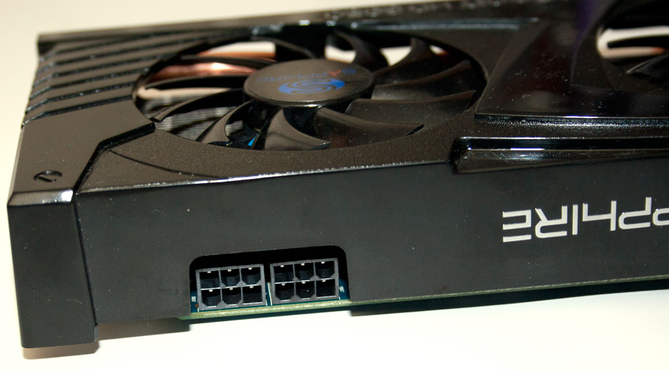
Don’t be fooled into thinking that the 6870 and 6850 are direct replacements for the outgoing cards though, as the benchmark results will testify: things aren’t that straightforward. This is confused slightly by the fact that the 5770 and 5750 will continue as is.
The Radeon HD 6870 uses the ‘Barts XT’ core for its shenanigans, which is a slightly refined take on the 5800 series core.
You’ll have to wait until the 6900 cards packing the ‘Cayman’ core for a truly radical makeover, which will hit the shelves in a month’s time.
In the meantime, this more-mainstream card is a cross between the 5830 and 5850. You get the full-fat 32 ROPs as found on the 5850, but with a core configuration of 1,120 stream processor, as found inside the 5830.
This tweaked core operates at a far higher clock rate to either of these predecessors though, cranking along at 900MHz, as opposed to the 750MHz of the 5850 and the 5830’s 800MHz.
In real terms this means that the 6870 is faster than the 5850, but it’s notably slower than the 5870. As we said, don’t be fooled by the name.
There’s more to AMD’s new chips than simply upping the frequency of its core though, and the previous years dominance of the DirectX 11 market has ushered in a new era for developers working with AMD.
Eyefinity, for instance, has been welcomed with open arms, with games developers embracing the extra screen space offered by the technology to build more immersive games. Something ably demonstrated at the 6870 launch event, where everything from Civ V through to Medal of Honor to Deus Ex: Human Revolution was demonstrated using Eyefinity.
It’s not just a case of developers stretching the viewport either, as the UI has been controlled to stay on the main screen where applicable. Eyefinity isn’t for everyone, but for those with the desktop space, it’s an obvious way of upgrading your visuals.
TODAY’S BEST DEALS
- 1
Current page:
AMD Radeon HD 6870 — Benchmarks
Next Page AMD Radeon HD 6870 — Benchmarks
TechRadar is part of Future US Inc, an international media group and leading digital publisher. Visit our corporate site .
©
Future US, Inc. Full 7th Floor, 130 West 42nd Street,
New York,
NY 10036.
Overview of AMD Radeon HD 6870
- Introduction
- Characteristics table
- AMD HD 6870 architecture
- Appearance
- PCB
- Cooling system
- Test bench
- List of measuring and control devices and tools used
- Instrumentation and testing procedure
- Temperature, noise level and electricity consumption.
- Acceleration
- Test results
- 3DMark Vantage
- Far Cry 2
- Call of Duty: World at War
- S.T.A.L.K.E.R.: Call of Pripyat
- Unigine Heaven
- Dirt 2
- Metro 2033
- Stone Giant
- Battlefield Bad Company 2
- Aliens vs Predator 3
- Temperature versus fan speed studies.
- Conclusion
At the end of the summer we had to say goodbye to the Canadian roots of the AMD graphics division, and, apparently, in vain. Surveys conducted on several foreign websites revealed an ambiguous attitude of respondents to such a decision. More than half of the participants regret that they will no longer see the familiar inscription, while no less part no longer associates the three-letter abbreviation with video cards. In other words, ATi remember and don’t want to forget. Then why was it necessary to abandon a well-known brand? Perhaps AMD believes that it is time to wean experienced and hardened consumers from the outdated name, because all young , as it were, have already got used to the AMD prefix, and often they don’t even remember about ATi at all.
But wait! All AMD/ATi graphics cards are still branded «Radeon». What is double standards? A double situation has developed for the authors’ description of components: correct — «ATi HD 5850», incorrectly — «AMD HD 5850», and for freshly released graphics adapters, the opposite is true. To be honest, it doesn’t take long to get confused. Maybe we should simplify it to a simple Radeon set-top box, and after six months — a year, return to the name of the manufacturer. Based on the same surveys, 3/4 tend to consider ATi / AMD video cards to be Radeons, and who made them is not so important.
This autumn, contrary to familiar traditions, video cards of the middle price segment were the first to appear, designed to expand the range of positions on the market rather than completely replace the existing ones. If before between $179 and $229 AMD didn’t have a single acceptable option, now there is an attractive Radeon HD 6850. So, HD 5850 and HD 6870 will coexist on the market until a certain time. Naturally, as the warehouses are depleted, the first one will disappear from the shelves.
Don’t get hung up on the manufacturer’s «recommended price», it’s just for comparison. In reality, the amount required for the purchase directly depends on market conditions and seasonality ( …or, speaking without cleverness, the greed of the seller and all those who accompany video cards to showcases — ed. ).
|
Characteristics |
HD 5830 |
HD 5850 |
HD 5870 |
HD 6850 |
HD 6870 |
GTX 465 |
GTX 470 |
GTX 480 |
| Codename |
Cypress LE |
Cypress Pro |
Cypress XT |
Barts Pro |
Barts XT |
GF100 |
GF100 |
GF100 |
| Process technology, nm |
40 |
40 |
40 |
40 |
40 |
40 |
40 |
40 |
| Size cores/cores, mm 2 .  |
334 |
334 |
334 |
255 |
255 |
<500 |
<500 |
<500 |
| Quantity transistors, mln. |
2154 |
2154 |
2154 |
1800 |
1800 |
3200 |
3200 |
3200 |
| Core clock, 2D|3D, MHz |
157 | 800 |
157 | 725 |
157 | 850 |
100 | 775 |
100 | 900 |
50/100 | 607/1215 |
50/100 | 607/1215 |
50 / 100 | 702/1402 |
| Voltage on the core, 2D|3D, V |
0.  95 | 1.15 95 | 1.15 |
0.95 | 1.10 |
0.95 | 1.15 |
0.96 | 1.21 |
0.96 | 1.21 |
0.9 | 1.05 |
0.9 | 1.0 |
0.96 | 1.05 |
| Number of shaders (PS), pcs. |
1120 |
1440 |
1600 |
960 |
1120 |
352 |
448 |
480 |
| Number of ROP units , pcs. |
16 |
32 |
32 |
32 |
32 |
32 |
40 |
48 |
| Number of texture units (TMU), pcs.  |
56 |
72 |
80 |
48 |
56 |
44 |
56 |
64 |
| Maximum fill speed , Gpx/s |
12.8 |
23.2 |
27.2 |
24.8 |
28.8 |
19.5 |
24.3 |
33.6 |
| Maximum fetch rate textures, Gtex/sec |
44.8 |
52.2 |
68 |
37.2 |
50.4 |
26.7 |
32.  4 4 |
42.1 |
| Pixel/Version Tex Shader Version |
5.0 / 5.0 |
5.0 / 5.0 |
5.0 / 5.0 |
5.0 / 5.0 |
5.0 / 5.0 |
5.0 / 5.0 |
5.0 / 5.0 |
5.0 / 5.0 |
| Memory type |
GDDR5 |
GDDR5 |
GDDR5 |
GDDR5 |
GDDR5 |
GDDR5 |
GDDR5 |
GDDR5 |
| Effective memory frequency , 2D|3D, MHz |
1200 | 4600 |
1200 | 4000 |
1200 | 4800 |
300 | 4000 |
300 | 4200 |
67 | 3206 |
67 | 3306 |
67 | 3700 |
| Voltage on memory, 2D|3D, V |
1.  6 | 1.6 6 | 1.6 |
1.6 | 1.6 |
1.6 | 1.6 |
1.6 | 1.63 |
1.6 | 1.6 |
1.57 | 1.6 |
1.57 | 1.6 |
1.57 | 1.6 |
| Memory capacity, MB. |
1024 |
1024 |
1024 / 2048 |
1024 |
1024 |
1024 |
1280 |
1536 |
| Memory bus, bit |
256 |
256 |
256 |
256 |
256 |
256 |
320 |
384 |
| Memory bandwidth , Gb/s |
147.  2 2 |
128 |
153.6 |
128 |
134.4 |
102.6 |
133.9 |
177.4 |
| Power consumption , 2D|3D, W |
24 | 175 |
27 |170 |
27 |188 |
15 |127 |
19| 151 |
nd | 200 |
nd | 215 |
nd | 250 |
| Crossfire / SLi |
Yes |
Yes |
Yes |
Yes |
Yes |
Yes |
Yes |
Yes |
| Card size (LxWxH), mm |
282x100x38 |
244x100x37 |
282x100x38 |
233x100x37 |
248x100x37 |
270x100x38 |
270x100x38 |
270x100x38 |
| MSRP $ |
229 |
299 |
399 |
179 |
239 |
279 (229) |
349 (259) |
499 |
recommendations
It’s quite reasonable to think that several cards are the main rivals for the AMD HD 6870. This is the HD 5830, and after the markdown to $229 and GTX 465. Another pair will be slightly more expensive: HD 5850 and GTX 470. Fierce competition for buyers’ wallets sooner or later leads to forced markdowns. Let’s hope that this fall or winter there will be an opportunity to “snatch” Cypresses leaving the stage.
The basic GPU design approach has not changed compared to previously released graphics cores. To appreciate the innovations, or better to say modifications, it is reasonable to take a look at the Barts XT block diagram once.
And compare it with Cypress…
At first glance, everything is the same, but take a closer look at the areas of stream processors. The Barts core consists of 14 SIMD cores, while Cypress has 20. But less does not mean worse: unlike the «big brother», both HD 68xx cards, as if in an orchestra, have not one conductor, but two (Ultra threaded dispatch processor). On their «shoulders» lies the work on the uniform distribution of tasks for superscalar processors.
In addition to the increased number of «managers», the number of «subordinates» has decreased — in order to improve efficiency, the number had to be sacrificed. However, I believe that physically the Barts GPU chip contains 20 SIMDs, but is artificially limited to 14. A full-fledged GPU will most likely be called AMD HD 6990 and will consist of two graphics cores.
But the differences don’t stop there. I propose to make a short journey into the history of the creation of the most successful invention of ATi / AMD so far — the R600.
Introduced in 2007 in the form of the Radeon HD 2900 Pro and XT, it was a progressive superscalar solution that defined the look of modern AMD GPUs for many years to come. For a more detailed study, let’s move on to the comparison.
|
|
R600 |
RV770 |
Cypress |
Barts |
| Schematic |
|
|
|
|
| Name |
Thread Processor (5 lane superscalar shader processor) |
Thread Processor (5 lane superscalar shader processor) |
Thread Processor (5 lane superscalar shader processor) |
Thread Processor (5 lane superscalar shader processor) |
Number of Single Precision FMAD units, pcs. |
four |
four |
four |
four |
| Instruction format |
VLIW |
VLIW |
VLIW |
VLIW |
| Number of SFU (Super Function Unit) units, pcs. |
one |
one |
one |
one |
| Number of FMAD units with double precision operations, pcs. |
0 |
one |
one |
0 |
| Number of stream processors, pcs. |
5 |
5 |
5 |
5 |
Peak number of floating point operations (FP), pcs. |
ten |
ten |
ten |
ten |
| GPU frequency, MHz |
742 |
750 |
850 |
900 |
Each block is based on 5 «scalars» capable of processing up to four instructions: one complex (sin, cos, etc.), four simple, up to two double precision (FP64). By analogy with the R600, in order to save the transistor budget, Barts is deprived of FP64 support. Thus, if we do not take into account the new technical process, then the modern core of a mid-budget video card is a reduced and overclocked copy of the R600.
|
|
R600 |
RV770 |
Cypress |
Barts |
| Schematic view |
|
|
|
|
| Name |
SIMD Core |
SIMD Core |
SIMD Core |
SIMD Core |
Number of processors, pcs. |
16 |
16 |
16 |
16 |
| Granularity, units |
64 |
64 |
64 |
64 |
| Total memory size, KB |
eight |
16 |
32 |
32 |
| Number of Single Precision FMAD units, pcs. |
64 |
64 |
64 |
64 |
| Number of SFU (Super Function Unit) units, pcs. |
16 |
16 |
16 |
16 |
Number of FMAD units with double precision operations, pcs. |
0 |
16 |
16 |
0 |
| Number of stream processors, pcs. |
80 (16×5) |
80 (16×5) |
80 (16×5) |
80 (16×5) |
| Peak number of floating point operations (FP), pcs. |
160 |
160 |
160 |
160 |
| Number of texture filtering units, pcs. |
four |
four |
four |
four |
With the introduction of modern lithographic technical processes, AMD managed to fit into one SIMD additional cache memory, which is vital for DX 11. Otherwise, there is only a systematic decrease in the GPU.
|
|
R600 |
RV770 |
Cypress |
Barts |
| Schematic view |
|
|
|
|
| Number of processor units, pcs. |
four |
ten |
twenty |
fourteen |
| Total memory size, KB |
0 |
16 |
64 |
64 |
| Number of texture filtering units, pcs. |
16 |
40 |
80 |
56 |
| Number of Single Precision FMAD units, pcs. |
256 |
640 |
1280 |
896 |
| Number of SFU (Super Function Unit) units, pcs. |
64 |
160 |
320 |
224 |
| Number of FMAD units with double precision operations, pcs. |
0 |
160 |
320 |
0 |
| Sum of stream processors, pcs. |
320 (80×4) |
800 (80×10) |
1600 (80×20) |
1120 (80×14) |
| Peak number of floating point operations (FP), pcs. |
640 |
1600 |
3200 |
2240 |
| Max. floating point performance (FP), TFLOPS. |
0.475 |
1.2 |
2.72 |
2.02 |
| Number of tessellation blocks, pcs. |
one |
one |
one |
one |
| Number of rasterization blocks, pcs. |
one |
one |
2 |
2 |
The main goal — saving core space — was achieved by reducing the number of SIMDs, but the amount of total cache memory was left at the same level. In parallel, to compensate for the performance of Barts in relation to Cypress, we increased its frequency. After the upgrade, the core of the new video card is well adapted to existing gaming tasks, and also wins in complexity (number of transistors per mm 2 ) and the area of competitor GF104.
After all the above words, someone will definitely have a slight feeling of deja vu. Apparently, the fate of the nVidia G92 is somewhat similar to the R600 and subsequent stages of modernization. But I dare to disappoint you, parts of the ATi / AMD GPU are not cubes and balls that can be manipulated and create new combinations to the required parameters. Reworking the existing core design requires new calculations, simulations, prototypes, etc. After a cycle of work, you will have to release a pilot batch and test it for a long time, and based on current prices, a GPU upgrade costs at least $30-35 million.
Subscribe to our channel in Yandex. Zen or telegram channel @overclockers_news — these are convenient ways to follow new materials on the site. With pictures, extended descriptions and no ads.
Review of the MSI Radeon HD 6870 video card on the new GPU Barts XT GECID.com. Page 1
::>Video cards
>2010
> MSI R6870-2PM2D1GD5
03-11-2010
Page 1
Page 2
One page
Not so long ago we published an article about a new line of video cards Radeon HD 6800 series. It covered all aspects of the new technologies used in the accelerators of this line, as well as the improvements that video cards based on the Barts core have undergone. It was noted that the expected process change to 32nm did not happen. The next generation AMD Radeon HD 6800 series graphics chips will still be manufactured according to the old 40nm process technology, the beginning of which can be considered the presentation of the Radeon HD 4770, which took place back in April 2009of the year. The entire line of Radeon HD 5000 also used 40nm technology. It’s all to blame, as Eric Demers, CTO of the GPU division at AMD, said, “the commitment to a well-developed process technology at the moment is due to economic reasons. Given the percentage of working dies they are getting today, the company is faced with the choice of mass-producing two 32nm or three 40nm GPUs at the same price.” Given this fact, in the near future AMD will most likely abandon 32nm and start mastering production using 28nm technology.
Without changing the manufacturing process, it will be problematic for AMD to position Barts as a significant step forward. Mainly, the new Barts GPU differs from its predecessor by major changes in the area of architecture optimization, performance increase per watt and millimeter of area, which improves overall efficiency. It also improved the main shortcomings of the previous ATI Radeon HD 5800 series, related to the low performance of tessellation and geometry processing. As mentioned earlier in our reviews, it was these two shortcomings that became the most serious problem for AMD video cards compared to competing NVIDIA graphics accelerators.
The AMD Radeon 6800 line was originally expected to replace the AMD Radeon 5800, but this did not happen. As you can see from the above diagram, there are practically no differences between the Barts and Cypress kernels. However, a simple calculation of the number of SIMD engines speaks eloquently to us about the significantly lower performance of the updated Barts XT GPU in relation to the Cypress core (Radeon HD 5870).
|
AMD Radeon HD 6870 |
AMD Radeon HD 6850 |
ATI Radeon HD 5870 |
ATI Radeon HD 5850 |
ATI Radeon HD 5830 |
ATI Radeon HD 4870 |
|
|
Codename |
Barts XT |
Barts PRO |
Cypress | Cypress | Cypress |
RV770 |
|
Number of transistors |
1. |
1.7 billion |
2.15 billion |
2.15 billion |
2.15 billion |
0.956 billion |
|
Number of stream processors |
1120 |
960 |
1600 |
1440 |
1120 |
800 |
|
Performance, TFLOPs |
2 |
1.5 |
2.72 |
2.09 |
1.79 |
1.2 |
|
Texture blocks |
56 |
48 |
80 |
72 |
56 |
40 |
|
Texture filtering, GTexels/s |
50. |
37.2 |
68 |
52.2 |
44.8 |
30 |
|
Number of ROPs |
32 |
32 |
32 |
32 |
16 |
16 |
|
Pixel filtering, GPixels/s |
28.8 |
24.8 |
27.2 |
23.2 |
12.8 |
12 |
|
Z/Stencil, GSamples/s |
115. |
99.2 |
108.8 |
92.8 |
51.2 |
48 |
|
Core frequency, MHz |
900 |
775 |
850 |
725 |
800 |
750 |
|
Memory frequency, GHz |
1.05 (4.2 GHz effect) GDDR5 |
1.0 (4.0 GHz effect) GDDR5 |
1.2 (4.8 GHz effect-I) GDDR5 |
1.0 (4.0 GHz effect) GDDR5 |
1.0 (4.0 GHz effect) GDDR5 |
900 MHz (3. |
|
Memory bus width |
256 bit |
256 bit |
256 bit |
256 bit |
256 bit |
256 bit |
|
Memory bandwidth, GB/s |
134.4 |
128 |
153.5 |
128 |
128 |
115.2 |
|
Frame buffer |
1 GB |
1 GB |
1 GB |
1 GB |
1 GB |
1 GB |
|
Process |
TSMC 40 nm |
TSMC 40 nm |
TSMC 40 nm |
TSMC 40 nm |
TSMC 40 nm |
TSMC 55 nm |
|
Maximum / minimum power consumption, W |
151/19 |
127/19 |
188/27 |
151/27 |
175/25 |
160/90 |
|
Recommended value |
$239 |
$179 |
~$349 |
~$229 |
~$200 |
N/A |
 7 billion
  4
4  2
2  6 GHz effect) GDDR5
 The Radeon HD 6870 GPU uses fourteen SIMD engines, each consisting of four texture units and sixteen stream processors. One stream processor has five ALUs (stream cores). This gives the GPU a total of 1120 stream cores with 56 texture units. The result of GPU processing is output through four clusters of the output part of the rendering pipeline. Each cluster has eight ROPs (raster operations) for a total of thirty-two ROPs. The 256-bit memory interface is provided by four 64-bit memory controllers.
The architecture numbers and specification of the Radeon HD 6870 graphics cards are very similar to those of the Radeon HD 5830, but with a doubling of the final part of the rendering pipeline. However, on the downside, the Radeon HD 6870 uses the same final rendering pipeline as the Radeon HD 5870, but fewer shader cores. For the Radeon HD 5830, the main drawback was just the halved number of ROPs, which caused performance delays. The Radeon HD 6870 can be called a modified and improved reincarnation of the Radeon HD 5830 graphics processor. In its equipment, the Barts XT core received as many as two UTDP (Ultra-Thread Dispatch Processor) controllers, while Cypress had only one, and part of the GPU responsible for processing tessellation algorithms. Such changes should provide an almost twofold superiority of the new solution in processing tessellation streams over graphics accelerators of the previous series.
Another significant improvement that the Radeon HD 6870 has due to the optimized die structure is the ability to operate at higher frequencies, which significantly affects the final performance. The Radeon HD 6870 is clocked at 900 MHz, which means the simplified Barts GPU core runs at a significantly higher clock speed than the Radeon HD 5830 or even the Radeon HD 5850. This increase in frequency leads to an increase in overall GPU performance by almost 25% compared to the Radeon HD 5850 running at 725 MHz. As a result, the smaller number of ALUs and texture units in the Radeon HD 6870 compared to the Radeon HD 5850 is fully compensated by the increased frequency of the GPU core, which practically equalizes their performance.
All of these improvements allow the Radeon HD 6870 to perform better than the Radeon HD 5850 with 25% less die area. This change clearly reduces idle power consumption and the production cost of the core itself as a whole. These two clear advantages should have a positive impact on the popularity of the final product. The memory of the Radeon HD 6870 runs at its native frequency of 1050 MHz (effective 4200 MHz), slightly faster than the Radeon HD 5850 (1000 MHz). The retail price for the Radeon HD 6870 is $240, which is slightly less than the $260 for the Radeon HD 5850.
Theoretical information is very encouraging, but you always want to get concrete results in test applications. For these purposes, the video accelerator MSI Radeon HD 6870 (R6870-2PM2D1GD5) got into our laboratory. The model provided by MSI is a complete copy of the reference sample produced at AMD factories. It is for this reason that our review and testing, in fact, will describe the reference solution Radeon HD 6870 from AMD.
Specification
There is nothing unusual in the specification, all the characteristics of the reference solution have already been listed by us above, now it is only worth repeating them for a specific copy sold under the MSI trademark.
|
Model |
MSI Radeon HD 6870 (R6870-2PM2D1GD5) |
|
|
Graphics core |
AMD Radeon HD 6870 (Barts XT) |
|
|
Conveyor |
1120 unified flow |
|
|
Supported APIs |
DirectX 11 (Shader Model 5.0) |
|
|
Core frequency, MHz |
900 |
|
|
Size (type) of memory, MB |
1024 (GDDR5) |
|
|
Memory frequency (effective), MHz |
1050 (4200) |
|
|
Memory bus bit |
256 |
|
|
Tire standard |
PCI Express X16 2. |
|
|
Maximum resolution |
Up to 4 displays of 1920×1200 each |
2x DVI-I (VGA via adapters) |
|
HDCP support |
Yes |
|
|
Drivers |
Fresh drivers can be downloaded from: |
|
|
Manufacturer website |
http://ua.msi.com/ |
 1
1 The table shows several innovations that the “reference” Radeon HD 6870 video cards have come to have. The DisplayPort 1.2 port allows you to display an image on several monitors at once using a special hub , and each monitor can be set to a different resolution. Supports up to four displays with resolutions up to 1920×1200 each. However, in total, up to six monitors can be connected to the accelerator using two hubs and two DVI-I connectors, but with a resolution of up to 1600×900.
The presence of HDMI 1.4 will allow the user to take advantage of 3D stereo transmission technology, which is necessary for connecting 3D monitors. Support for new OpenGL 4.1 and AMD HD3D technologies has appeared, as well as AMD Eyefinity and AMD EyeSpeed technologies already familiar to us from the 5800 series of accelerators. Such a variety of new possibilities for using the accelerator will be a worthy response from AMD to partially similar technological solutions proposed by NVIDIA in the 400 series.
The video accelerator is presented in a tight box. Its design emphasizes the ability to work with MSI’s proprietary overclocking utility Afterburner. The company’s logo is visible at the top, and on the right side, the GPU manufacturer AMD RADEON GRAPHICS is mentioned, which indicates the release of this line by AMD, and not by ATI (AMD) as it was before. Below is the R6870 graphics core itself, the accelerator has 1 GB GDDR5 memory, DirectX 11 support and the presence of two mini DisplayPort connectors on the rear panel. Up to four screens can be connected to mini DisplayPort connectors via a special hub using AMD Eyefinity technology. At the very bottom, there are logos of the product supporting MSI proprietary overclocking technologies and the use of capacitors of increased reliability and durability on the PCB board.
The last two features are described in more detail on the back of the box.
Here, at the top, the model of the R6870-2PM2D1GD5 graphics accelerator is indicated, and below, support for the MSI Afterburner utility is described in detail, which allows you to overclock both one accelerator and several installed in CrossFireX mode. It is possible to save overclocking profiles, as well as profiles with reduced frequencies of the video card, which leads to energy savings and reduced heat dissipation, and therefore a decrease in the total system noise. Below is the use of solid capacitors in this model, which guarantee 10 years of trouble-free operation. On the right are the main advantages of this accelerator in 30 languages. The packaging leaves the impression of a high-quality finished product and has full information about the internal contents.
The delivery set of MSI Radeon HD 6870 (R6870-2PM2D1GD5) is quite worthy:
- Two adapters from two peripheral power connectors to one 6-pin video card power connector;
- CrossFire Bridge;
- CD with drivers and utilities;
- Brief instructions for installing a video card;
- mini DisplayPort to DisplayPort adapter;
- DVI to VGA adapter.
Quite a justified set that provides 80% of the requests of an ordinary user. But to connect a group of displays here, you will obviously have to purchase the necessary adapters or a special hub, with simultaneous support for up to four monitors.
Compared to NVIDIA’s flagship GeForce GTX 480 graphics card, AMD’s new solution looks more elegant. This is not only the first impression, but judging by the announced innovations by AMD, accelerators based on the Radeon HD 6870 should feature two times lower power consumption with comparable performance in some applications. The video card Radeon HD 6870 differs from the «top» solutions of both manufacturers in shorter length, it has, like the Radeon HD 5870, two 6-pin auxiliary power connectors located on the upper end of the video card. Connecting additional power will not cause inconvenience, and the wires themselves will not interfere with the installation of the video card, increasing its length due to the connectors themselves and the wires extending from them.
Surprisingly, the reference sample only has one CrossFire connector. Most likely, later, there will be solutions from another manufacturer that have two CrossFire connectors, which are very useful for increasing the overall performance of the video system when this accelerator is connected in CrossFireX modes together with other similar models.
The rear part of the AMD Radeon HD 6870 video card does not have any technological holes, everything is covered with a plastic casing, which harmoniously complements the overall design of the accelerator. It’s nice that the power connectors are turned up — this allows the accelerator to be compatible with a large number of cases.
The reverse side of the accelerator did not receive a single significant element.
Thanks to the two-slot design of the cooling system, five display connectors (2x DVI-I, HDMI 1.4, 2x mini DisplayPort 1.2) fit on the back of the accelerator. There is also a fairly large grill for removing hot air from the case. Such a variety of connection connectors will provide AMD Radeon HD 6870 with full compatibility with all modern offers on the market for display devices.
On the front side of the printed circuit board, you can highlight the graphics processor and the eight video memory chips surrounding it. Here are all the elements of the GPU power system and accelerator memory.
The GPU frequency is 900 MHz. The Barts XT chip itself is made according to the 40 nm process technology and contains 1120 universal shader pipelines and thirty-two rasterization units, and data exchange between the graphics core and memory is carried out via a 256-bit bus.
When there is no load, the chip operation frequency drops to 100 MHz, and the video memory slows down to 81 MHz (324 MHz effective frequency). At the same time, the supply voltage is also reduced, which provides a noticeable reduction in power consumption and temperature.
Video memory with a total capacity of 1 GB is based on eight Hynix H5GQ1h34AFR T2C GDDR5 chips with an access time of 0.8 ns, which allows them to operate at an effective frequency of up to 5000 MHz. Since the resulting frequency of the memory chips on the video card is slightly lower and amounts to 4200 MHz, there remains a good frequency corridor in reserve, which, we hope, can be used during overclocking.
The accelerator has a 4+2-phase power supply. Here, four phases go to the GPU and are implemented using the Chil CHL8214 controller, which has support for the I2C protocol. This protocol should provide softvoltmod using the new version of the MSI Afterburner utility. The MSI Afterburner 2.0.0 utility that came with the video card did not allow changing the voltage on the GPU.
The cooling system itself consists of two parts. The metal casing through the thermal interface comes into contact with all hot elements of the board: video memory chips and elements of the power subsystem. A separate design is used to cool the GPU — a massive aluminum radiator with three copper heat pipes of different diameters, which are soldered to a copper plate that is in contact with the GPU chip. The central copper tube of increased diameter should contribute to more efficient heat dissipation from the GPU die. The thermal interface is quite viscous, which should also have a positive effect on the overall efficiency of the cooling system. The turbine-type fan, which has a standard size, is more than enough to cool the GPU. In general, the cooling system can be called improved and more technologically advanced compared to the reference turbine used on hot models of the 5800 series.
We used the FurMark utility to evaluate the efficiency of the cooling system, and detailed monitoring was carried out using GPU-Z and MSI Afterburner.
Working at stock frequencies and controlling the turbine speed automatically, the GPU warmed up to 82°C. Considering that the turbine rotation speed was only 35% of the maximum and the entire cooler was running quietly, we can talk about the low heat dissipation of the accelerator and the excellent operation of the «reference» cooling system in automatic mode.