Amd athlon 2100 xp: AMD Athlon XP 2100+ Specs

AMD’s Athlon XP 2100+ Processor


AMD’s Athlon XP 2100+ Processor
Crunching Code at 1733MHz.

By, Marco Chiappetta
March 13, 2002

For about three years now, a fierce battle has been raging between Intel and AMD.  This battle has taken consumers down a road that led to a wider selection of higher performing processors than ever before, and at prices that were much lower than previous generations of flagship CPUs.  As each company introduced a new speed step, or introduced a new processor core, the competition was right there to introduce their new part in an effort to steal some thunder and make some noise of their own.    The Athlon arrived and quickly became the first «mainstream» CPU to break the 1GHz barrier, enticing a large part of the enthusiast community in the process.  Then Intel stepped up to bat and were the first to reach the 2GHz mark.  These two X86 rivals have also been battling on price.  With every press release from AMD announcing their latest price cuts, came a similar announcement from Intel.  It seems that the «one-upmanship» between these two companies will never end.  Today, only two months after introducing the Athlon XP 2000+, AMD unleashes their latest soldier, the Athlon XP 2100+.  The core technology remains unchanged but the clock speed has been bumped up another 66MHz, bringing AMD’s current flagship CPU to 1733MHz.  What do you say we get this CPU installed into one of our test beds and see just what it can do?

Specifications of the AMD Athlon XP 2100+ Processor
A few more clock cycles and some nice green packaging. ..

           
CLICK IMAGES FOR ENLARGED VIEW

Key Architectural Features of the AMD Athlon? XP Processor:

  • QuantiSpeed? Architecture for enhanced performance

  • Nine-issue superpipelined, superscalar x86 processor microarchitecture designed for high performance

  • Multiple parallel x86 instruction decoders

  • Three out-of-order, superscalar, fully pipelined floating point execution units, which execute x87 (floating point), MMX? and 3DNow!? instructions

  • Three out-of-order, superscalar, pipelined integer units

  • Three out-of-order, superscalar, pipelined address calculation units

  • 72-entry instruction control unit

  • Advanced hardware data prefetch

  • Exclusive and speculative Translation Look-aside Buffers

  • Advanced dynamic branch prediction

3DNow!? Professional technology for leading-edge 3D operation:

  • 21 original 3DNow!? instructions?the first technology enabling superscalar SIMD

  • 19 additional instructions to enable improved integer math calculations for speech or video encoding and improved data movement for Internet plug-ins and other streaming applications

  • 5 DSP instructions to improve soft modem, soft ADSL, Dolby Digital surround sound, and MP3 applications

  • 52 SSE instructions with SIMD integer and floating point additions offer excellent compatibility with Intel’s SSE technology

  • Compatible with Windows® XP, Windows 98, Windows 95, and Windows NT® 4. x operating systems

266MHz AMD Athlon? XP processor system bus enables excellent system bandwidth for data movement-intensive applications:

  • Source synchronous clocking (clock forwarding) technology

  • Support for 8-bit ECC for data bus integrity

  • Peak data rate of 2.1GB/s

  • Multiprocessing support: point-to-point topology, with number of processors in SMP systems determined by chipset implementation

  • Support for 24 outstanding transactions per processor

Other Architectural Elements:

  • The AMD Athlon? XP processor with performance-enhancing cache memory features 64K instruction and 64K data cache for a total of 128K L1 cache. 256K of integrated, on-chip L2 cache for a total of 384K full-speed, on-chip cache.

  • Socket A infrastructure designs are based on high-performance platforms and are supported by a full line of optimized infrastructure solutions (chipsets, motherboards, BIOS). Available in Pin Grid Array (PGA) for mounting in a socketed infrastructure Electrical interface compatible with 266MHz AMD Athlon XP system buses, based on Alpha EV6? bus protocol

  • Die size: approximately 37.5 million transistors on 128mm2. Manufactured using AMD’s state-of-the-art 0.18-micron copper process technology at AMD’s Fab 30 wafer fabrication facility in Dresden, Germany.

To demonstrate the main features differentiating the AMD Athlon XP from Intel’s Pentium 4, this table from AMD’s marketing team breaks things down for you.  The table is a bit dated though, as it lists features foe a «Willamette» based Pentium 4 that only has 1/2 of the amount of cache as the new Northwood Pentium 4 that is also currently available.

AMD has dubbed the combination of enhancements and features found in the Athlon XP line of CPUs, their «QuantiSpeed» Architecture.   
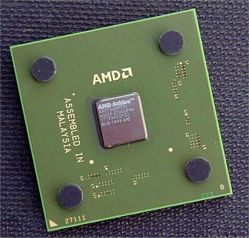
So, what exactly is «QuantiSpeed» all about?  We’ll let AMD tell the story.

QuantiSpeed? Architecture:
QuantiSpeed? architecture allows the AMD Athlon? XP processor to accomplish more instructions per clock cycle (IPC). Improved IPC is a result of the following technological advances.

Nine-issue, superscalar, fully pipelined microarchitecture:
Provides more pathways to feed application instructions into the execution engines of the core, allowing the processor to complete more work in a given clock cycle (high IPC). The delicate balance between the depth of the pathways and clock speed of the processor produces high levels of performance.

Superscalar, fully pipelined Floating Point Unit (FPU):
Completes more floating point operations per clock cycle than competitive x86 processors and permits high operating frequencies. The end result is a processor with the computing power to tackle the most computation-intensive software applications.

Hardware data prefetch:
Prefetches data from system memory to the processor’s Level 1 cache, which reduces the time it takes to feed the processor critical data, increasing work throughput and therefore overall performance.

Exclusive and speculative Translation Look-aside Buffers (TLBs):
Keep the maps to critical data close to the processor, which helps prevent the processor from stalling or waiting when future data is requested. These TLB structures are now larger, exclusive between caches, and speculative. Larger TLB’s give the AMD Athlon XP processor access to additional data maps. Exclusivity removes the duplication of information, freeing up more space in the Level 2 cache for other useful data to be used by the processor. And the speculative nature of these structures allows the processor to generate future maps of critical data quickly.

These four key advances allow AMD’s QuantiSpeed architecture to perform more calculations per second, boosting overall throughput.

Processor ID and Preliminary Tests


Athlon XP 2100+ [in 1 benchmark]


AMD
Athlon XP 2100+

Buy

  • Interface
  • Core clock speed
  • Max video memory
  • Memory type
  • Memory clock speed
  • Maximum resolution

Summary

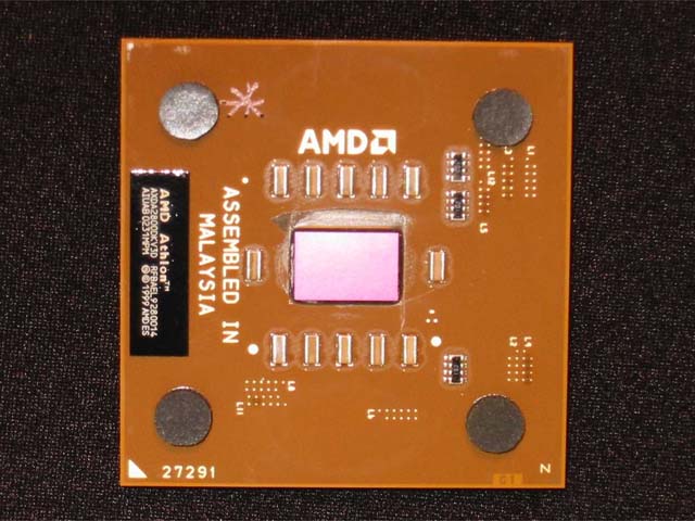
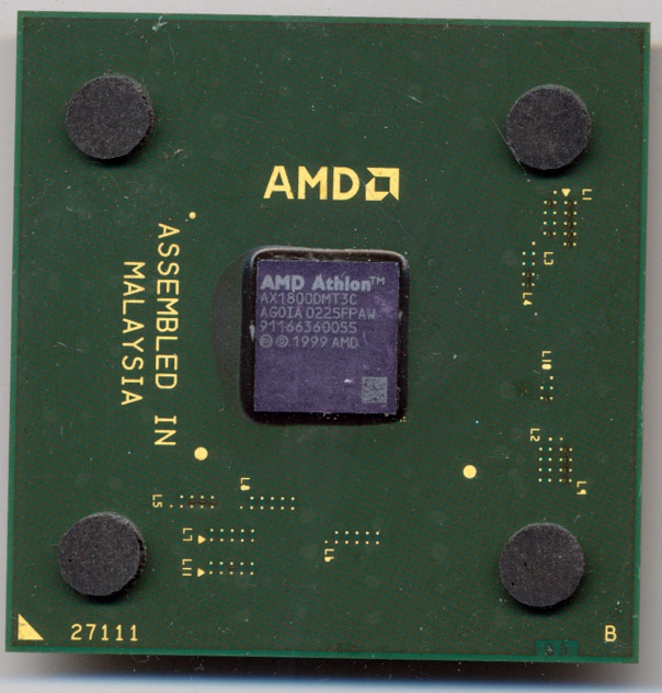
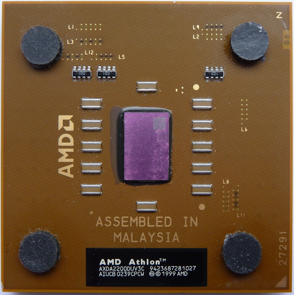
AMD started Athlon XP 2100+ sales on January 2001. Based on a Thoroughbred architecture, this desktop processor is primarily aimed at home systems. It has 1 core and 1 thread, and is based on 180 nm manufacturing technology, with a maximum frequency of 1733 MHz and a locked multiplier.

Compatibility-wise, this is AMD Socket A processor with a TDP of 72 Watt.

We have no data on Athlon XP 2100+ benchmark results.

General info


Athlon XP 2100+ processor market type (desktop or notebook), architecture, sales start time and pricing.

Place in performance ranking not rated
Market segment Desktop processor
Architecture codename Thoroughbred (2001−2002)
Release date January 2001 (22 years old)
Current price $47 of 14999 (Xeon Platinum 9282)

Technical specs


Basic microprocessor parameters such as number of cores, number of threads, base frequency and turbo boost clock, lithography, cache size and multiplier lock state. These parameters can generally indicate CPU performance, but to be more precise you have to review its test results.

Physical cores 1 (Single-Core)
Threads 1
Boost clock speed 1.73 GHz of 6 (Core i9-13900KS)
L1 cache 128 KB of 7475.2 (Apple M2 Pro 10-Core)
L2 cache 256 KB of 36864 (Apple M2 Max)
L3 cache 0 KB of 786432 (EPYC 7373X)
Chip lithography 180 nm of 4 (Ryzen 9 7940HS)
Die size 150 mm2
Number of transistors 37 million of 9900000 (Ryzen 5 7645HX)
64 bit support
Windows 11 compatibility

Compatibility


Information on Athlon XP 2100+ compatibility with other computer components and devices: motherboard (look for socket type), power supply unit (look for power consumption) etc. 
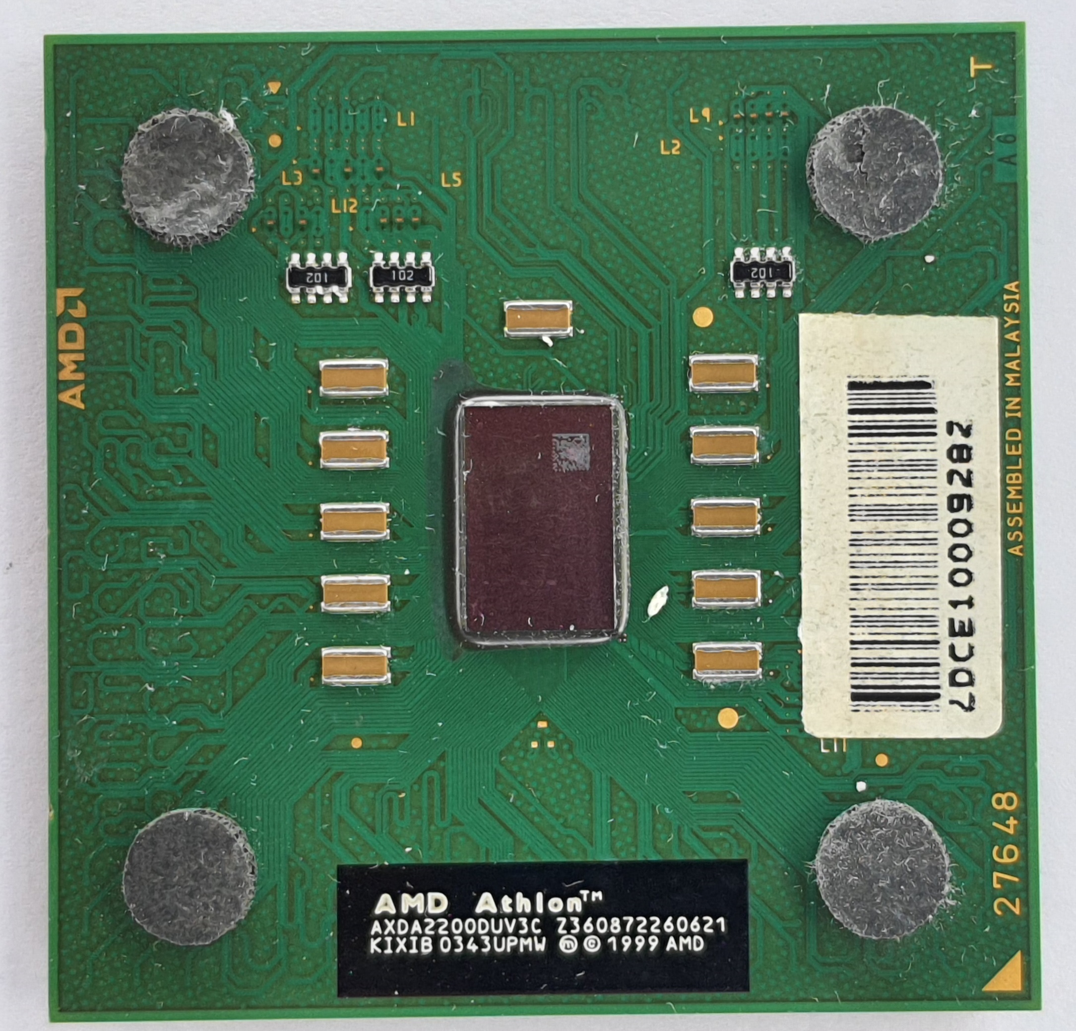
Useful when planning a future computer configuration or upgrading an existing one.

Note that power consumption of some processors can well exceed their nominal TDP, even without overclocking. Some can even double their declared thermals given that the motherboard allows to tune the CPU power parameters.

Number of CPUs in a configuration 1 of 8 (Opteron 842)
Socket A
Power consumption (TDP) 72 Watt of 400 (Xeon Platinum 9282)

Benchmark performance


Single-core and multi-core benchmark results of Athlon XP 2100+. Overall benchmark performance is measured in points in 0-100 range, higher is better.


    Passmark

    Passmark CPU Mark is a widespread benchmark, consisting of 8 different types of workload, including integer and floating point math, extended instructions, compression, encryption and physics calculation. There is also one separate single-threaded scenario measuring single-core performance.

    Benchmark coverage: 68%


    Athlon XP 2100+
    210


    Recommended GPUs

    People consider these graphics cards to be good for Athlon XP 2100+, according to our PC configuration statistics.


    GeForce3
    Ti200

    33.3%


    GeForce GTX
    560

    33.3%


    Radeon HD
    3650 AGP

    33.3%

    These are the fastest graphics cards for Athlon XP 2100+ in our user configuration statistics.

    There is a total of 3 configurations based on Athlon XP 2100+ in our database.


    GeForce GTX
    560

    33.3% (1/3)

    User ratings: view and submit


    Here is the rating given to the reviewed processor by our users.