AMD Athlon (K7) — CPU MUSEUM
K6-III ◄ Athlon (K7) ► Athlon XP
AMD Athlon K7 © HARDWARECOP
Athlon is the brand name applied to a series of x86-compatible microprocessors designed and manufactured by Advanced Micro Devices (AMD). The original Athlon was the first seventh-generation x86
processor and, in a first, retained the initial performance lead it had over Intel’s competing processors for a significant period of time. The
original Athlon also had the distinction of being the first desktop processor to reach speeds of one gigahertz (GHz). AMD has continued using the Athlon name with the Athlon 64, an eighth-generation processor featuring x86-64 (later renamed AMD64) architecture, and the Athlon II.
The Athlon Pluto/Orion is a cartridge-based processor, named Slot A and similar to Intel’s cartridge Slot 1 used for Pentium II and
Pentium III. It used the same, commonly available, physical 242 pin connector used by Intel Slot 1 processors but rotated by 180 degrees to connect
the processor to the motherboard.
|
AMD-K7800CPRBCA Specification Details |
Show | |
|
AMD-K7900MNR53B A Specification Details |
Show | |
The second generation Athlon, the Thunderbird, debuted on June 5, 2000. This version of the Athlon shipped in a more traditional pin-grid array (PGA) format that plugged into a socket
(«Socket A») on the motherboard (it also shipped in the slot A package). It was sold at speeds ranging from 600 MHz to 1.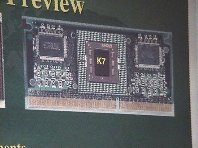 4 GHz (Athlon Classics using the Slot A package could clock up to 1 GHz).
The major difference, however, was cache design. Just as Intel had done when they replaced the old Katmai-based Pentium III with the much
faster Coppermine-based Pentium III, AMD replaced the 512 kB external reduced-speed cache of the Athlon Classic with 256 kB of on-chip, full-speed exclusive cache. As a general rule,
more cache improves performance, but faster cache improves it further still.
|
A0700MPR24B Specification Details |
Show | |
Kindly donated by Pauli Rautakorpi.
|
A0800AMT3B Specification Details |
Show | |
|
A0900AMT3B Specification Details |
Show | |
|
A0950AMT3B Specification Details |
Show | |
CPU-Z:
|
A1000AMT3B Specification Details |
Show | |
|
A1000AMT3C Specification Details |
Show | |
Kindly donated by Pauli Rautakorpi.
|
A1133AMS3C Specification Details |
Show | |
|
A1200AMS3B Specification Details |
Show | |
|
A1200AMS3C Specification Details |
Show | |
Kindly donated by Pauli Rautakorpi.
|
A1333AMS3C Specification Details |
Show | |
|
A1400AMS3C Specification Details |
Show | |
Unlisted models:
- Argon: 500 MHz, 550 MHz, 600 MHz, 650 MHz, 700 MHz
- Pluto/Orion: 550 MHz, 600 MHz, 650 MHz, 700 MHz, 750 MHz, 850 MHz, 950 MHz, 1000 MHz
- Thunderbird: 600 MHz, 650 MHz, 700 MHz, 750 MHz, 850 MHz, 1100 MHz, 1266 MHz, 1300 MHz
Sumbit a picture or contribute to the museum!
RETURN TO AMD
RETURN TO THE MAIN MUSEUM PAGE
AMD Athlon K7 retrospective | Custom PC
The summer of 1999 wasn’t a great time for Intel, and it really should have been. In February it had launched the Pentium III, a supercharged upgrade of the P6 microarchitecture. Cyrix, whose 6×86 processors had embarrassed some 1st-generation Pentiums, was effectively finished, its tech now in the hands of VIA Technologies.
That just left AMD, whose K6 line of processors had captured some of the budget PC market, but didn’t have the optimised pipelines, cache or floating point performance to give Intel any serious competition.
But when AMD released its first K7 Athlon processors to reviewers in June, something unexpected happened. Sure, there was already some buzz about the new ‘K7’ CPU, thanks to intriguing early demos and briefings, but a Pentium III killer? Not likely. Yet when the final production samples hit magazine labs and website testbenches, it became clear that the new Athlon was pretty special.
AMD’s chip wasn’t just matching Pentium III, clock speed for clock speed, but beating it. Worse, it was beating it in the kind of floating point intensive apps that Intel considered home territory, including 3D games. Athlon was kicking Intel right where it hurt, and that eye-watering discomfort wasn’t going to let up any time soon.
K7 comes together
How exactly did AMD manage this feat? Well, as with so many standout products in the hardware space, the answer involves several developments all coming together at the same time. On the one hand, the success of the K6 II and III had left AMD in a surprisingly strong position.
The K6 architecture had made the most of technology bought in with the company’s 1996 acquisition of NexGen and had pumped money into AMD’s war chest. It had also cemented AMD’s position as Intel’s most credible rival.
What’s more, AMD also had new CPU and bus technology developed by the Digital Equipment Corporation (DEC) for its Alpha RISC processors. It had even taken on most of DEC’s RISC CPU design team, including key architects, Dirk Meyer and Jim Keller.
Thanks to a patent cross-licensing deal with Motorola, AMD also had a head start on new copper-based die manufacturing technologies, not to mention a new chip fab in Dresden on its way to use them. This would become important later on.
All this helped lead to a revolutionary design – the first 7th-generation x86 processor. The original 0.25-micron (250nm) Athlon had a die with over 22 million transistors – the highest transistor count of any x86 processor to date. It also had an ingenious split cache system, with 128KB of on-chip L1 cache operating at clock speed, plus another 512KB of L2 cache included in the processor module.
This L2 cache operated at a fraction of the clock speed – half-speed on the initial models – but with breathing room to scale to cover higher and slower speeds later on. This arrangement gave Athlon a performance advantage over the earlier K6 processors, even before you factored any other architectural improvements into the equation.
But these improvements were just as significant. Meyer, Keller and their team designed an architecture that was capable of decoding three x86 instructions simultaneously and – crucially – symmetrically, unlike the Pentium III.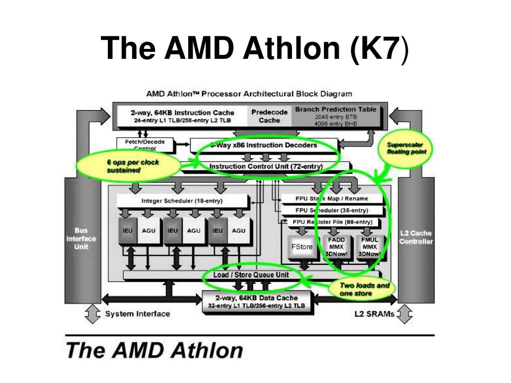
True, the Pentium III’s instruction pipeline could handle three simple instructions at once, but feed it more than one lengthy, complex instruction and it choked, as only one pipeline could manage the workload. The Athlon, by contrast, could chew through three complex instructions without any trouble. You got three instructions at a time, every time.
What’s more, the design featured a new level of optimised branch prediction, which was not only more accurate in guessing what the next operation would be, but faster to recover when it got that guess wrong.
Like the team brought in from NexGen, the team brought in from DEC had serious skills and experience in RISC chip design, and AMD put this to good use. The Athlon architecture converted x86 instructions into more efficient ‘macro ops’ and then those ‘MOPS’ into RISC operations, which the CPU’s execution units could work on, nine to a clock.
This design was incredibly efficient by the standards of the day, but it was also conducive to scaling upwards. Where the K6-III had been stuck at 500MHz, the Athlon launched at 500, 550 and 600MHz speeds, matching the 600MHz of Intel’s top-end Pentium III. As if that wasn’t enough, AMD added a 650MHz version in fewer than six weeks after launch. The final kicker was that AMD was no longer second rate on floating point operations.
Not only were the Athlon’s floating point units (FPUs) much faster than the weedy FPUs of the K6 line, but AMD built on the SIMD instructions of its 3DNow! Technology, with 24 new instructions on top of the original 21. Most mimicked the cache and streaming controls seen in Intel’s mighty SSE tech, but AMD also bundled in new DSP and complex maths extensions, plus MP3 and Dolby Digital decoding tools. This chip was built to game and entertain.
There was one final way that AMD now matched Intel – the Athlon was AMD’s first chip to abandon sockets and embrace the slot. AMD’s Slot-A connector harnessed DEC’s EV6 bus and bus protocol, which allowed for burst data transfers at double the rate of Intel’s equivalent GTL+, giving you a whopping 1. 6GB/sec of bandwidth between the CPU and the motherboard chipset.
The Athlon’s front side bus operated at double the 100MHz speed of the memory bus, and as faster RAM became available, this gave AMD scope to up the FSB speed even further, to 266MHz or even 400MHz. What’s more, with a slot design, AMD could combine its CPU die and L2 cache in the one package, and that package was a whole lot easier to fit. And to make sure dozy upgraders didn’t try to stuff AMD CPUs into Intel slots or vice versa, it cleverly reversed the physical design.
Awesome Athlon
Talk about architectures and specs was all very well, of course, but nothing really prepared those of us benchmarking PCs in the late 1990s for the sheer undeniable awesomeness of Athlon. The results of benchmarks wouldn’t have made comfortable reading for Intel, especially once the Athlon 650 rolled out in August. Both the Athlon 600 and Athlon 650 were faster than the Pentium III 600 in Quake III: Arena, whether paired with the hero graphics chip of the day – Nvidia’s Riva TNT2 – or with 3dfx’s still speedy Voodoo 3.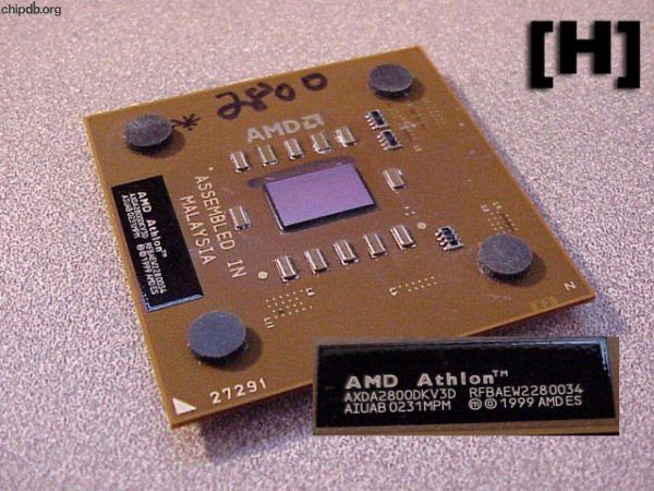
The Athlon was around 10 per cent faster in standard Windows applications, and up to 20 per cent faster in gaming benchmarks. The Athlon 600 was 10fps faster than the Pentium III 600 in the fiendishly demanding Quake II Crusher benchmark. As further tests from the likes of AnandTech proved, even a Pentium III overclocked to 650MHz couldn’t keep up.
And this was just the beginning. In September, Intel launched the Pentium III 600B – a variant of the ‘Katmai’ Pentium III with a 133MHz front side bus. It couldn’t match the Athlon 550 in many benchmarks, let alone the 600 and 650MHz versions, and still lagged behind the Athlon in when it came to gaming performance.
In October, AMD responded with a 700MHz Athlon that pulled even further ahead. AnandTech’s benchmarks of the time put it 20 per cent faster than the Pentium III 600B in the Quake II Crusher benchmark. It was nearly 27 per cent ahead in Quake III.
It was only with the launch of its Coppermine Pentium III processors in October 1999 that Intel could claw back the lead. Yet while the Pentium III 733EB was now king of the hill, an Athlon 700 could still benchmark faster in many tests than Intel’s 700MHz Coppermine Pentium III.
As the clock speeds rose, the competition just grew hotter. In November 1999, AMD launched a new series of Athlons with a 0.18-micron (180nm) K75 core, taking the top speed up to 750MHz. In January and February, these were followed with 800 and 850MHz CPUs. Then just as Intel geared up to launch a (gasp!) 1GHz Coppermine Pentium III in March 2000, AMD stole its thunder by launching the Athlon 1000. To really take the proverbial, it did it two days earlier, giving AMD the first 1000MHz x86 CPU.
Athlon was first, but it wasn’t fastest. The Pentium III 1000EB was actually ahead of the Athlon 1000 in many tests, partly due to superior SSE support in many popular benchmark games.
Yet there was only a few frames per second in it, and Athlon systems often had the edge on price. What’s more, the Pentium III 1000 was only available to system builders at the time of launch. Anyone could get their hands on the 1GHz Athlon at the time.
Issues and overclocks
Of course, no new CPU comes without teething troubles. Early buyers found a range of compatibility issues with specific hardware, partly because Athlon was a complex, power-hungry CPU, and partly because of AGP slot power issues affecting many motherboards and driver issues with the latest Nvidia cards. With certain VIA chipsets and less consistent power supplies, you could find yourself in a world of instability. Nvidia even released a driver update for its graphics chips that disabled the high-performance 2x mode on the AGP slot when Athlon was detected.
Some enthusiasts were also disappointed with the Athlon’s limited overclocking potential. The K6 line had been a treat for overclockers – gamers upped 450MHz CPUs to 600MHz routinely, and there was much debate in PC magazines about whether we should allow manufacturers to send in pre-overclocked systems.
The Athlon wasn’t having any of that. The only ways to overclock the original CPUs were to crack open the modules and interfere manually with the resistors, or to purchase a third-party ‘Goldfingers’ device which did it all for you. Through either method you could increase your multiplier and give your Athlon a healthy speed boost, although it meant invalidating your warranty along the way.
The age of Athlon
The Athlon set the stage for a golden age of PC CPUs. Intel struck back with Coppermine, then AMD replaced the K7’s old aluminium interconnects with copper, and ran the L2 cache at the full speed of the CPU. The 2nd-generation Athlon ‘Thunderbird’ processors could match and even beat the Coppermine Intel Pentium IIIs, causing Intel to push even further with its Coppermine T CPUs.
Before we knew it, 1GHz was starting to look like old hat. 1333MHz and 1400MHz were the new targets. Meanwhile, the K7 architecture was making waves at the budget end. Where Intel’s cheap, cache-less Celeron processors couldn’t handle Deus Ex, Half-Life or Unreal Tournament, AMD’s K7 Duron CPUs were storming through them.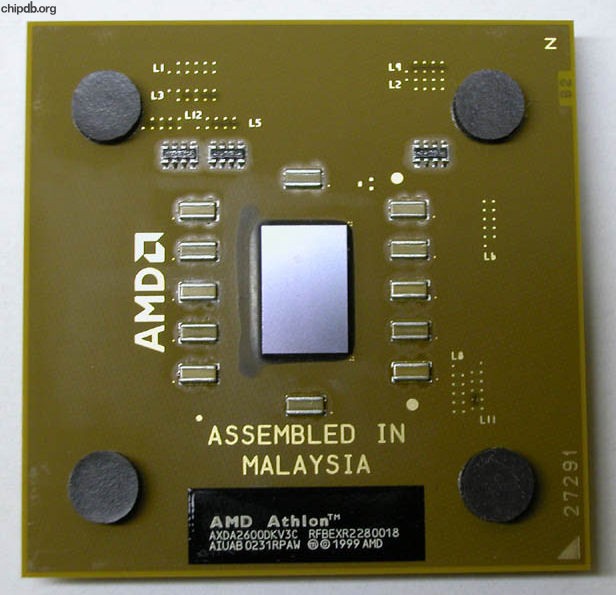
There’s still a lot of affection for the Athlon in the PC enthusiast community. At a time when Intel seemed unassailable, it was the first chip to really knock it off its feet. This made Intel try a little harder, and the result was that everybody won. In fact, it’s a mark of that affection that when AMD created a new budget Zen-based processor line-up in 2018, it still used the Athlon brand, with the Athlon 3000G coming out in November 2019. It’s a sign of a classic brand when it’s still being used 20 years later.
The first generation of AMD K7, now just history
September 9, 2005, Friday
00:19
I.N.
for section
Laboratory
My recently released
the first work dedicated to AMD processors.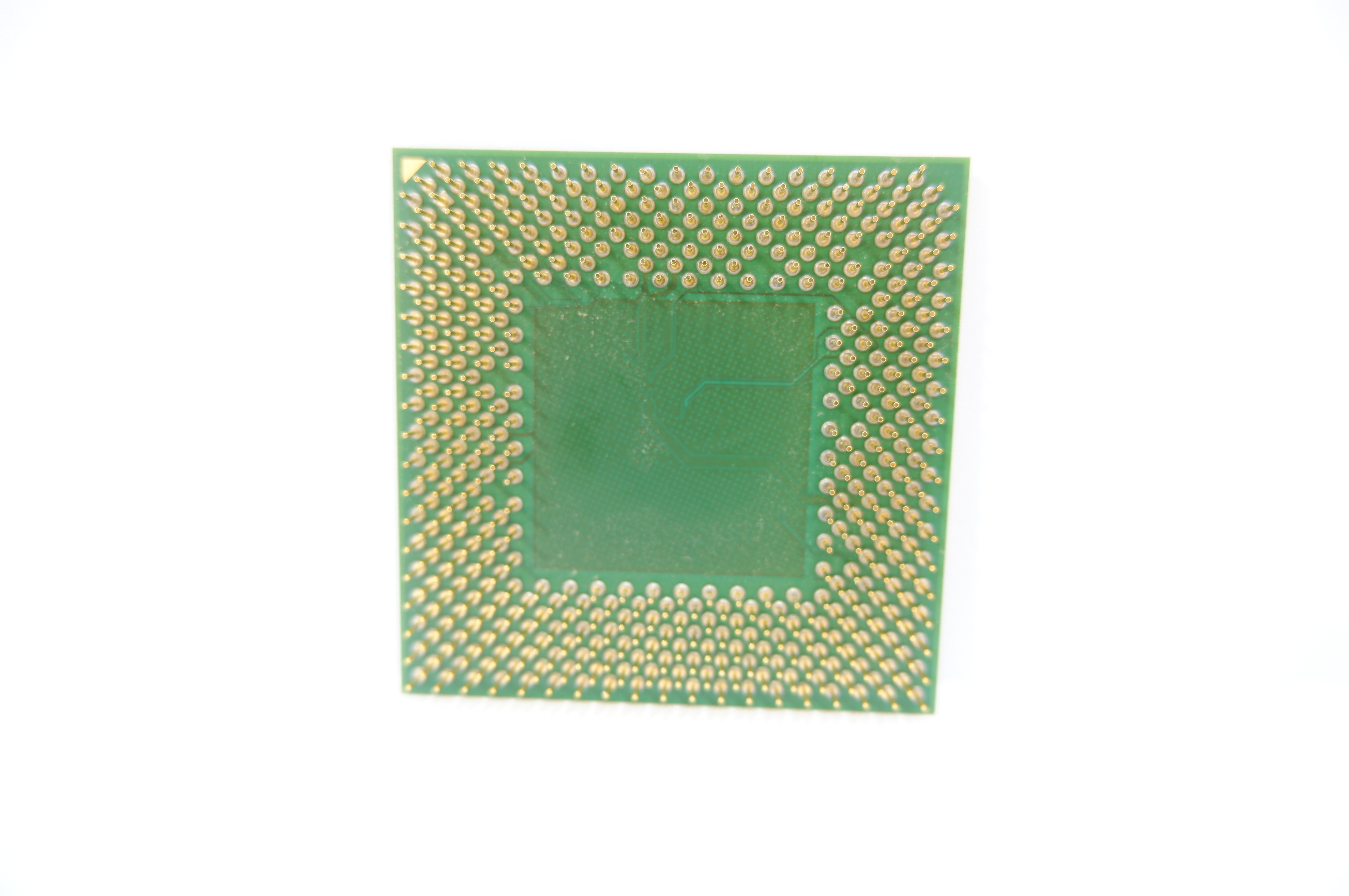 The article covered modern processors of the K7 generation (all Duron, Sempron and Athlon XP) and the new K8. However, in the forum dedicated to the discussion of this work, wishes began to appear to expand the article and describe older processors. Today’s article is purely about old Slot A and Socket A processors in addition to the first one.
The history of the K7 architecture began with a presentation by Dirk Meyer at the Microprocessor Forum at 1998 of a new core codenamed Argon. The first Athlon Model 1 (K7) based on the Pluto core (however, the core of younger models was sometimes called the Argon name) with a 250nm manufacturing process was announced on June 23, 1999 and was released in August of the same year. A little later, Athlon Model 2 (K75) appeared on the Orion core with a 180nm process technology.
In general, the technical innovations of the first K7 processors are as follows:
- the maximum processor core temperature is 70°C
- First level cache (L1) is 128 KB (64 KB for data and 64 KB for instructions)
- instruction set 3DNow! extended to 45 commands (Enhanced 3DNow!)
- extended, compared to previous generations, block MMX instructions
- There are three integer calculation pipeline units, which allows the execution of three integer instructions simultaneously
- There are three Floating Point Units (FPUs) that allow three floating point instructions to be executed simultaneously
- manufacturing process 250 nm, a little later — 180 nm.
The
Athlon «B» 1000 Thunderbird with 100 MHz bus and 1 GHz along with 900 and 950 MHz models was announced on March 6, 2000, two days before the PIII 1GHz, becoming the world’s first «home» gigahertz processor.
The first chipset was AMD’s own 750 chipset. It consisted of the AMD 751 northbridge and the AMD 756 southbridge. Later, the VIA KX133 chipset also came out — it added support for AGP 4X and PC133 memory (up to 2GB). The next AMD 760 chipset changed the type of memory used to DDR (DDR1600 and DDR2100). Its problem was the lack of the possibility of asynchronous clocking of the bus and memory frequencies — and the processor and memory had to work synchronously at a bus frequency of 200 or 266 MHz, up to 4 GB of memory was supported. For Socket A, VIA released an updated version of its chipset — KT133 (in fact, only the northbridge was redesigned, the southbridge remained the same), a little later than KT133A (support for FSB266 was added). All other specs are the same as the KX133.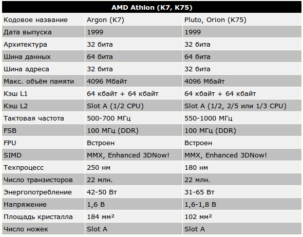
Pluto and Orion have a 512 KB Level 2 (L2) cache located on the processor board and operating at a partial processor frequency. The board itself is packed in a special cartridge. The bus frequency is 100 MHz, but data is being transmitted on both edges of the signal (DDR), so the effective data rate is 200 MHz.
AMD K75-Athlon Orion
Athlon Thunderbird Slot A
In 2000, Model 4 Thunderbird Slot A was released. Its main difference is that the cache is integrated into the processor core and operates at its full frequency, but its size is reduced to 256 kb. The technical process is 180 nm. It should be noted that this model was planned for computer manufacturers, and not for the retail market.
GoldFinger («Golden Finger») — this module was used to overclock Slot A processors, allowing you to change the multiplier and voltage, the only disadvantage of using it is the need to open the cartridge and, as a result, the loss of warranty.
| Model | Core | Process (nm) | FSB (MHz) | L2 cache frequency (MHz) | Level 2 cache (L2) | Core voltage (V) | Maximum heat dissipation (W) | Maximum current consumption (A) |
| Athlon 500 | Pluto | 250 | 100 | 250 | 512 | 1.6 | 42 | 27.4 |
| Athlon 550 | Pluto | 250 | 100 | 275 | 512 | 1.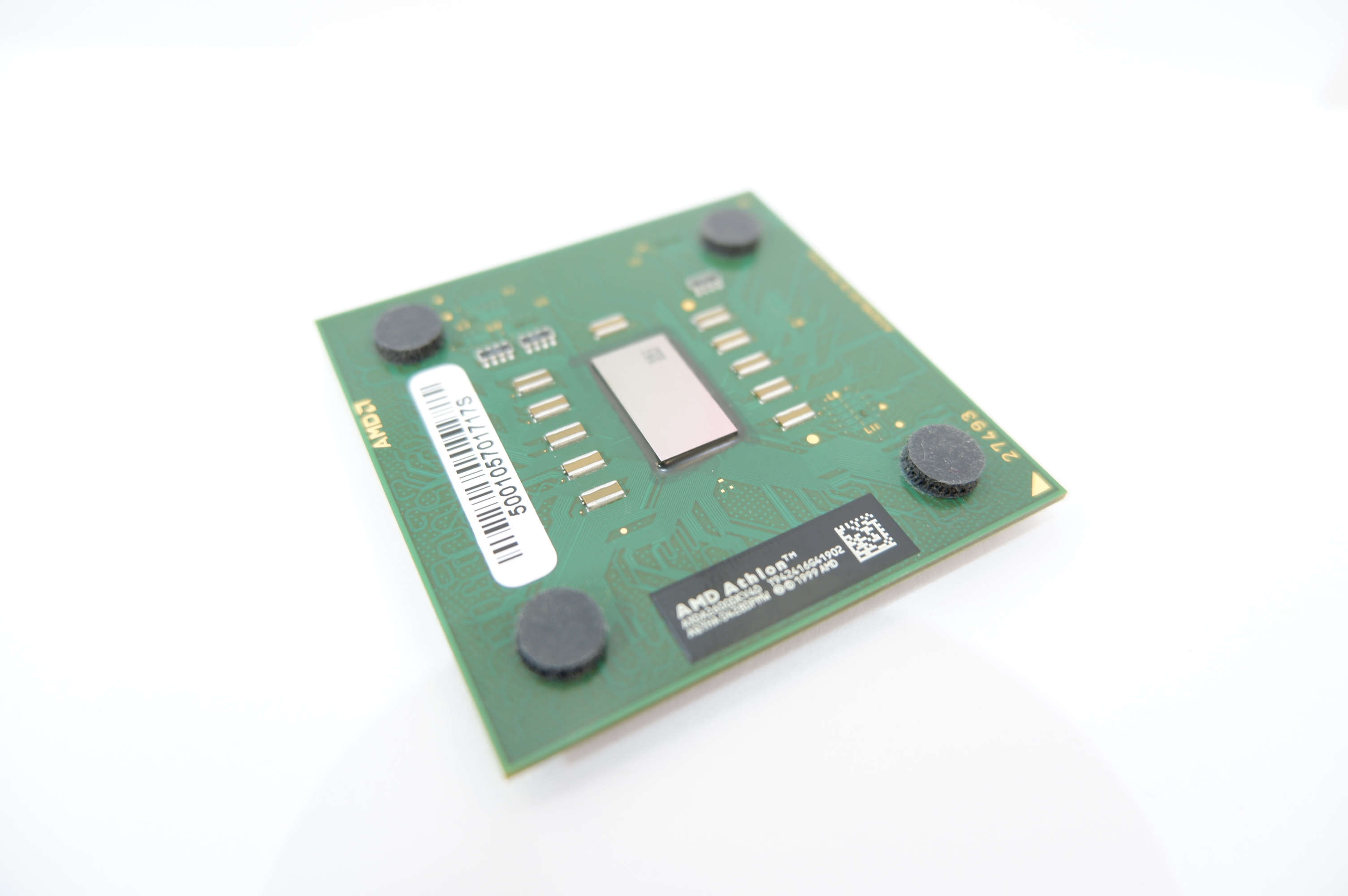 6 6 |
46 | 30.1 |
| Orion | 180 | 100 | 275 | 512 | 1.6 | 31 | 20 | |
| Athlon 600 | Pluto | 250 | 100 | 300 | 512 | 1.6 | 50 | 32.9 |
| Orion | 180 | 100 | 300 | 512 | 1.6 | 34 | 21.5 | |
| Athlon 650 | Pluto | 250 | 100 | 325 | 512 | 1.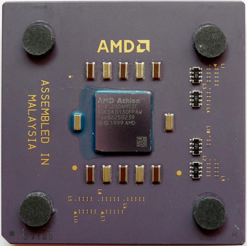 6 6 |
54 | 35.5 |
| Orion | 180 | 100 | 325 | 512 | 1.6 | 36 | 22.9 | |
| Thunderbird | 180 | 100 | 650 | 256 | 1.7 | 36.1 | 23.8 | |
| Athlon 700 | Pluto | 250 | 100 | 350 | 512 | 1.6 | 50 | 33.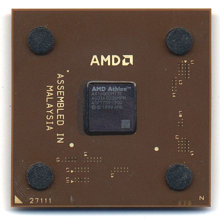 1 1 |
| Orion | 180 | 100 | 350 | 512 | 1.6 | 39 | 24.4 | |
| Thunderbird | 180 | 100 | 700 | 256 | 1.7 | 38.3 | 25.2 | |
| Athlon 750 | Orion | 180 | 100 | 300 | 512 | 1.6 | 40 | 25.8 |
| Thunderbird | 180 | 100 | 750 | 256 | 1. 7 7 |
40.4 | 26.6 | |
| Athlon 800 | Orion | 180 | 100 | 320 | 512 | 1.7 | 48 | 29.5 |
| Thunderbird | 180 | 100 | 800 | 256 | 1.7 | 42.6 | 28 | |
| Athlon 850 | Orion | 180 | 100 | 340 | 512 | 1.7 | 50 | 30 |
| Thunderbird | 180 | 100 | 850 | 256 | 1.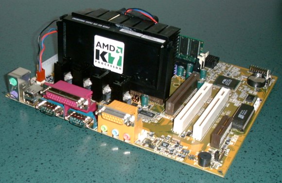 7 7 |
44.8 | 29.4 | |
| Athlon 900 | Orion | 180 | 100 | 300 | 512 | 1.8 | 60 | 34 |
| Thunderbird | 180 | 100 | 900 | 256 | 1.75 | 49.7 | 31.7 | |
| Athlon 950 | Orion | 180 | 100 | 316 | 512 | 1.8 | 62 | 35 |
| Thunderbird | 180 | 100 | 950 | 256 | 1.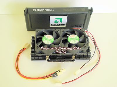 75 75 |
52 | 33.2 | |
| Athlon 1000 | Orion | 180 | 100 | 333 | 512 | 1.8 | 65 | 37 |
| Thunderbird | 180 | 100 | 1000 | 256 | 1.75 | 54.3 | 34.7 |
In June 2000, the first member of the Socket A family, the Athlon Model 4 Thunderbird Socket A, enters the market.
Athlon «C» 1000 Thunderbird with 133 MHz bus
They also had a black backing, like my Athlon 900, which, under a voltage of 1.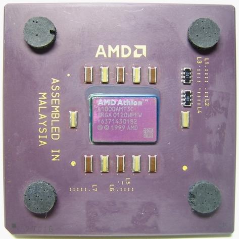 8V, worked on a 127MHz bus — almost 1.15GHz in total.
The bus frequency is 100 and 133 MHz, but data is being transmitted on both edges of the signal (DDR), so the effective data rate is 200 and 266 MHz, respectively.
| Model | Core | FSB (MHz) | Level 2 cache (L2) | Core voltage (V) | Maximum heat dissipation (W) | Maximum current consumption (A) |
| Athlon «B» 650 | Thunderbird | 100 | 256 | 1.7 | 38 | 23 |
| Athlon «B» 700 | Thunderbird | 100 | 256 | 1. 7/1.75 7/1.75 |
38.3/40.0 | 25.2/23.0 |
| Athlon «B» 750 | Thunderbird | 100 | 256 | 1.7/1.75 | 40.4/43.0 | 26.6/25.0 |
| Athlon «B» 800 | Thunderbird | 100 | 256 | 1.7/1.75 | 42.6/45.0 | 28.0/26.0 |
| Athlon «B» 850 | Thunderbird | 100 | 256 | 1.7/1.75 | 44.8/47.0 | 29.4/27.0 |
| Athlon «B» 900 | Thunderbird | 100 | 256 | 1.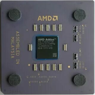 75 75 |
50 | 29 |
| Athlon «C» 900 | Thunderbird | 133 | 256 | 1.75 | 50 | 29 |
| Athlon «B» 950 | Thunderbird | 100 | 256 | 1.75 | 52 | 30 |
| Athlon «B» 1000 | Thunderbird | 100 | 256 | 1.75 | 54.3 | 34.6 |
| Athlon «C» 1000 | Thunderbird | 133 | 256 | 1. 75 75 |
54 | 31 |
| Athlon «B» 1100 | Thunderbird | 100 | 256 | 1.75 | 60 | 34 |
| Athlon «C» 1100 | Thunderbird | 133 | 256 | 1.75 | 60.3 | 34 |
| Athlon «C» 1133 | Thunderbird | 133 | 256 | 1.75 | 62.1 | 36 |
| Athlon «B» 1200 | Thunderbird | 100 | 256 | 1.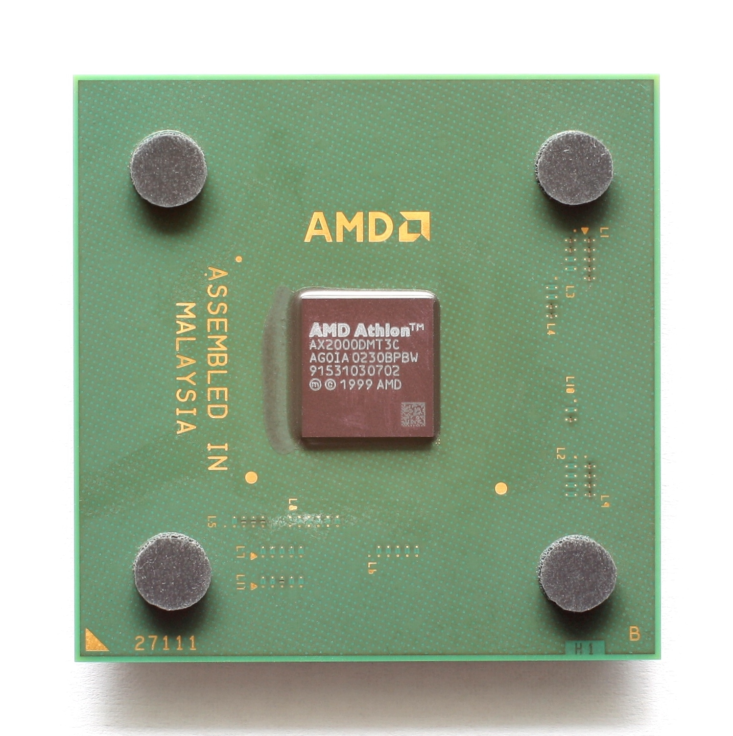 75 75 |
66 | 38 |
| Athlon «C» 1200 | Thunderbird | 133 | 256 | 1.75 | 65.7 | 37 |
| Athlon «C» 1266 | Thunderbird | 133 | 256 | 1.75 | 66.9 | 38 |
| Athlon «B» 1300 | Thunderbird | 100 | 256 | 1.75 | 68 | 39 |
| Athlon «C» 1333 | Thunderbird | 133 | 256 | 1.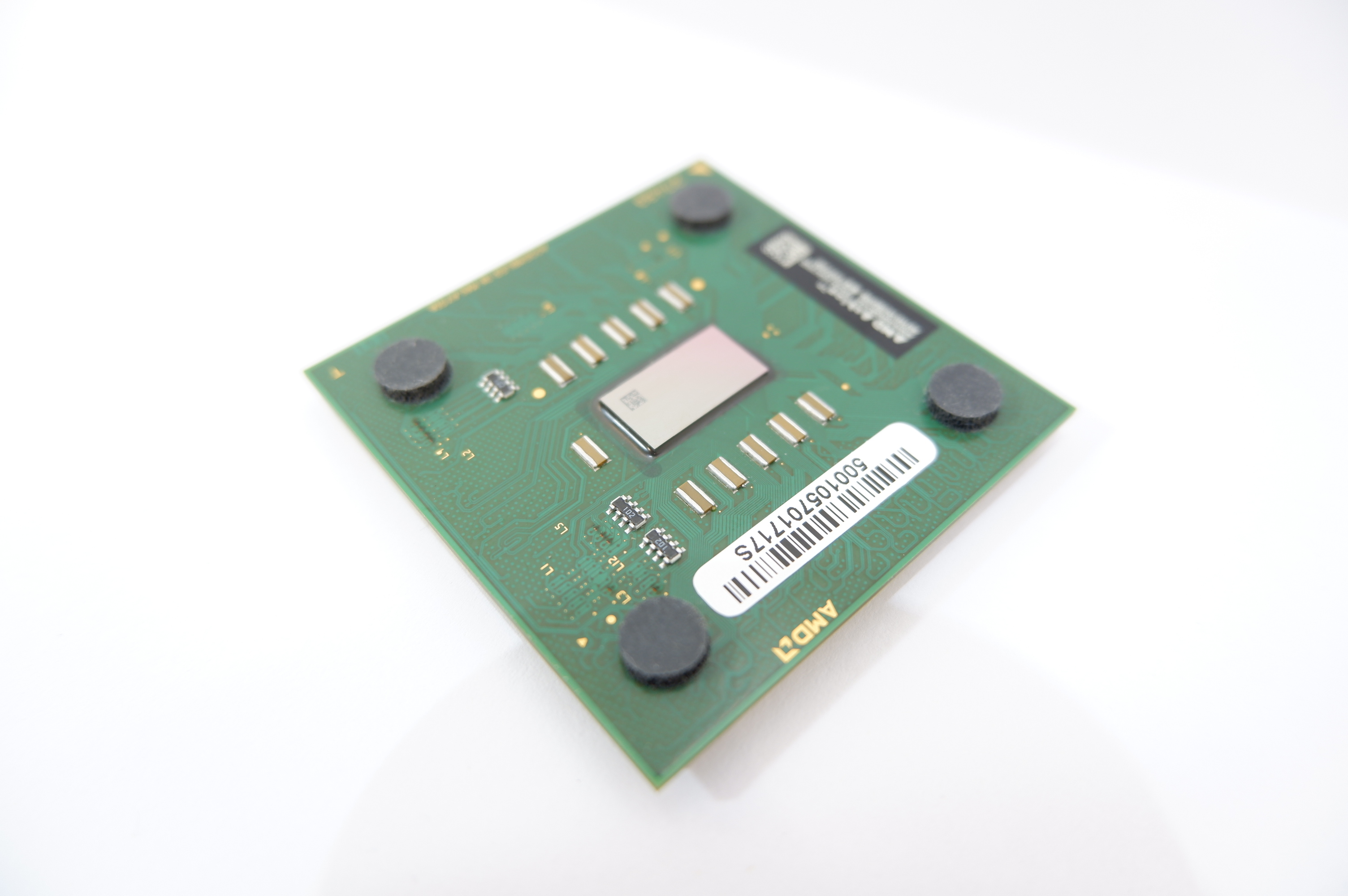 75 75 |
69.8 | 39.9 |
| Athlon «B» 1400 | Thunderbird | 100 | 256 | 1.75 | 72.1 | 42 |
| Athlon «C» 1400 | Thunderbird | 133 | 256 | 1.75 | 72.1 | 42 |
Sites from which information was used in one way or another:
- amd.com
- amdclub.ru
- amdclub.narod.ru
- interdacom.ru
- soft-service.ru
- thg.ru.
As well as own knowledge and experience :).
I.N.
Subscribe to our channel in Yandex. Zen or telegram channel @overclockers_news — these are convenient ways to follow new materials on the site. With pictures, extended descriptions and no ads.
Rate material
rating: 3.8
out of 5
votes: 33
Section materials feed
MSI RadiX AX6600 Router Overview
Retroclocking: LGA 775 All Stars — Full Afterburner
MSI Clutch GM31 Lightweight Wireless Gaming Mouse Review
MSI MEG Ai1300P PCIE5 power supply review and testing
Retroclocking: All-Star LGA 775
The first generation of AMD K7, now just history
Overview of the EPoX EP-9NPAJ SLI motherboard
Overview of memory modules Crucial Ballistix PC2-8000 (BL2KIT6464AA1005)
MSI Motherboard Specifications for Intel LGA775 Platform
An alternative look at CBO, or WC² project: Water Cooling / Water Closet
Unintentional review of Abit AL8 motherboard (i945P)
Interesting materials
Retroclocking: LGA 775 All Stars — Full Afterburner
July 11, 2023
You might be interested in
Effective advertising for your business
Russian «Geran», breaking through the air defense of the Odessa port, was able to hit the ship of the Navy of the Armed Forces of Ukraine
Already the fifth column of PMC «Wagner» is heading to Osipovichi and good quality photos have appeared on the network
Syrsky: Returning Bakhmut is a matter of honor, we simply have to recapture it for our brothers
Swedish Stridsvagn 122 tanks spotted in Donbas – what a modified Leopard 2A5 can do
India is considering the possibility of delivering the BrahMos
hypersonic cruise missile to Russia MWM: Ukrainian counter-offensive has seriously undermined confidence in the combat capabilities of Bradley and Leopard 2
90 007 A new one is moving to Belarus large convoy of PMC «Wagner» with 80 cars and trucks
Syrsky: We want to get quick results from the counteroffensive, but this is almost impossible
PMC «Wagner» fighters left the secret training base in the village of Molkino near Krasnodar
Innovative T-shirt will allow you to feel every blow to the upper body in Assassin’s Creed
Intel invested $ 9 million in the development of a humanoid robot
Syrsky again spoke about idea to surround Bahmut
Baldur’s Gate 3 contains 17 thousand possible endings0004 Ukraine decided to accuse Yanukovych of seizing power in 2010
Syrsky: The situation in the south is difficult, the RF Armed Forces have gathered more than 100,000 servicemen in the Kupyansk region
Twitter settings have blocked personal correspondence of many users
retaliation strike» on objects in Odessa and Nikolaev
In 2024, the peak of solar activity is expected — how the Sun can surprise scientists and Elon Musk
Ukraine intends to continue sea transportation of grain without the participation of Russia
Processors
Tires online shop.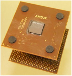 Stable stands and tripods for acoustic equipment and musical instruments.
AMD K7 architecture
- Details
- Parent category:
- Category: AMD K7
processors
architecture
The creation of the seventh generation K7 processor core in 1999 was a significant achievement for AMD. The Athlon processor features outstanding technical features: three parallel execution pipelines, a double frequency front-side bus with rising and falling data, an asynchronous memory bus, and highly intelligent decoder and data prefetch blocks.
The first-level cache includes a dual-channel partially associative (set-associative) instruction cache and a data cache with a capacity of 64 KB each. The K7 data cache provides simultaneous access to two 64-bit values when executing register load and memory write instructions. Another important feature of the K7 is the presence of a special pre-decoding cache in the instruction cache block, which is used by instruction decoders. Recall that in modern x86-compatible processors, direct execution of x86 commands does not occur, since they are inconvenient for achieving maximum performance. x86 instructions are decoded into simpler and more efficient internal fixed-length RISC-like instructions, which, in fact, are executed by the microprocessor.
There are three such decoders in the K7 core, and they work in parallel, so the pre-decode cache contributes significantly to increasing throughput.
In addition, the L1 instruction cache contains a two-level fast page forwarding TLB used to convert virtual to physical addresses: the L1 TLB has a capacity of 24 lines, and the L2 TLB has a capacity of 256 lines. A similar TLB in the first level data cache includes a first level TLB with a capacity of 32 lines and a second level TLB with a capacity of 256 lines. Finally, the first-level instruction cache contains a large branch prediction table with a capacity of 2048 lines, which makes it possible to achieve a high probability of correct dynamic branch prediction.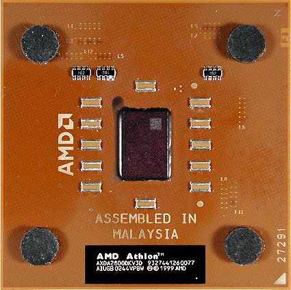
From the decoders, the commands enter the command control device with a capacity of 72 lines. AMD K7 is a superscalar microprocessor with out-of-order speculative instruction execution. The large capacity of the command control device makes it possible to efficiently use the resources of nine functional executive devices that are pipelined and capable of out-of-order execution of commands. These devices include three address pipelines, three integer pipelines, and three floating point pipelines. Accordingly, K7 can perform up to 9commands per clock. The total length of the integer pipeline in K7 is 10 stages, and the floating point pipeline is 15 stages.
The capacity of the integer instruction scheduler is 18 lines; through it, commands are sent to both integer and addressable functional units. A similar instruction scheduler for floating point numbers has a capacity of 36 lines. It is worth dwelling on the operation of the floating-point instruction block in more detail.
First of all, we note that this block provides operation with single (32 bits), double (64 bits) and extended (80 bits) precision. In addition, these functional actuators work with data in the MMX and 3DNow! instruction formats. The FSTORE actuator executes register loading and memory writing commands. The FADD block, in addition to adding floating-point operands, executes addition instructions from the 3DNow! and MMX shift commands. The FMUL block, in addition to multiplying floating-point numbers, executes MMX commands, 3DNow! and special division operations. Thus, the K7 can simultaneously perform floating point addition and multiplication in the FADD and FMUL blocks. This gives a peak performance of two real operations per clock.
Functional diagram of the K7 microarchitecture
- Details
- Parent category:
- Category: AMD K7
processors
architecture
The most important component that determines the performance of the microprocessor are the characteristics of the external cache in the second level and the external system bus of the processor. The dedicated bus between K7 and the L2 cache has a width of 64 bits plus 8 bits to support ECC codes. Theoretically, the maximum capacity of the second level cache in the K7 is 8 MB. The use of a 512 KB L2 cache in real Athlon processors is in a certain sense the most efficient, since the L2 cache controller integrated into the K7 contains full tags for a 512 KB cache, and with a larger cache capacity, the controller will contain only a part of the tag.
- Details
- Parent category:
- Category: AMD K7
processors
architecture
With the K7 microarchitecture, AMD engineers introduced support for SMP architectures for the first time. The protocol that maintains cache coherence in K7 is called MOESI (from the first letters of the possible cache states — Modify, Owner, Exclusive, Shared, Invalid). According to AMD, this protocol was first implemented in x8b-compatible processors.
The L1 cache in K7 has a separate port through which coherent traffic passes. Cache coherency support traffic is also separated from the main traffic on the system bus. Naturally, decoupling increases the effective throughput of the bus, and hence the efficiency of SMP configurations.
- Details
- Parent category:
- Category: AMD K7
processors
architecture
The AMD K7 bus has two great features. Firstly, this is not an ordinary common bus, but a switch. This solution provides guaranteed throughput for point-to-point connections, while conflicts are possible on a common bus. Secondly, the K7 system bus has a frequency of up to 400 MHz. With a bus width of 64 bits plus 8 ECC bits, it has a throughput of up to 3.2 GB/s. A high-speed bus is needed not only to support fast DDR RAM, but also to provide I / O streams from the PCI and AGP buses.
The K7 system bus interface is electrically compatible with the Alpha EV6 bus protocol. The K7 microprocessor is connected to the bus via the Socket A (Socket 462) interface. An important feature that affects the throughput of the K7 bus is the amount of packets transmitted over the bus. This bursting of data contributes to the pipelined processing of transactions on the bus. For the K7, the burst size is 64 bytes (the length of the cache line), which is twice that of the P6 generation processors. Separate transaction processing contributes to the efficient use of the system bus. It allows you to overlap the execution of various transactions in time, allowing you to start processing new transactions without waiting for the completion of the previous ones. Theoretically, the maximum capacity of bus-addressable RAM in the K7 is 8 TB, but in reality, chipsets support up to 4 GB.
- Details
- Parent category:
- Category: AMD K7
processors
architecture
In October 2001, the first Athlon processors based on the Palomino core entered the market. This modification was given the XP index (eXtreme Performance), emphasizing the innovations of the architecture in comparison with the «regular» Athlon.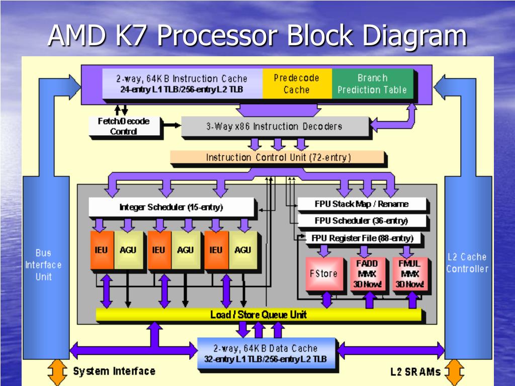 So, in particular, the mechanism for translating the addresses of commands and data into physical memory addresses has undergone a significant alteration. To speed up access to commands and data, all modern processors have a Translation Look-aside Buffer (TLB). This buffer caches, but not data or commands, but their physical addresses. In previous Athlon processors, this buffer was two levels. The first level (L1) has a capacity of 24 values for instruction addresses and 32 values for data addresses. The second level (L2) could store up to 256 data addresses and 256 instruction addresses.
The size of the first level buffer has been increased in the Palomino core, now it can store up to 40 data address values. In addition, now TLB, as well as the main cache, has become «exclusive» — exclusive. This means that the contents of the first level buffer do not duplicate the contents of the second level buffer. And finally, the new kernel implements a mechanism for loading new address values ahead of time (before they may be required) — speculatively reload.
Significantly improved mechanism for forward loading of data from memory to cache. This data-ahead mechanism was also implemented in early processors, but only for instructions included in 3DNow! and SSE. The core of Athlon XP processors continuously analyzes the addresses of the data requested by the processor and the sequence in which they were requested. Based on the analysis, an attempt is made to predict the addresses of the data that will be requested, and forward loading of this data into the processor cache. In many cases, for example, when cyclic processing of large data arrays, the prediction will be successful. This improves performance even for non-optimized applications.
Both the 3DNow! instruction system and the SSE instruction system are fully implemented in the Palomino kernel. This complex set is called 3DNow! professional technology.
These changes required another increase in the number of transistors — up to 37.5 million. However, this did not lead to an increase in power consumption.