AMD Ryzen 7 7800X3D Review: New Gaming Champ Beats Pricier CPUs
When you purchase through links on our site, we may earn an affiliate commission. Here’s how it works.
Sub-$450 CPU is even faster for gaming than Ryzen 9 7950X3D.
Editor’s Choice
(Image: © Tom’s Hardware)
Tom’s Hardware Verdict
The Ryzen 7 7800X3D is the fastest gaming chip available and easily beats more expensive competitors from both Intel and AMD’s own lineup. At an affordable $449 price point that will surely be reduced in the future, the Ryzen 7 7800X3D is the gaming chip to beat.
TODAY’S BEST DEALS
Cons
- —
No support for DDR4 memory
- —
Reduced performance in productivity apps
- —
No direct multiplier-based overclocking
- —
Expensive AM5 ecosystem
Why you can trust Tom’s Hardware
Our expert reviewers spend hours testing and comparing products and services so you can choose the best for you. Find out more about how we test.
Today’s best AMD Ryzen 7 7800X3D deals
$449.99
View
Show More Deals
The $449 eight-core Ryzen 7 7800X3D is the new high-performance gaming champion for the desktop PC. Even though the Ryzen 7 7800X3D is much less expensive than its competitors, it’s still 12% faster in gaming on average than Intel’s $580 flagship Core i9-13900K and up to 40% faster in some titles, and it also beats the fastest gaming CPU currently available — AMD’s own $699 16-core Ryzen 9 7950X3D.
AMD’s exotic second-gen 3D V-Cache tech powers the 7800X3D’s incredible gaming performance by boosting the chips’ L3 cache capacity to an incredible 96MB via a 3D-stacked chiplet, assuring it a top spot on our list of the best CPUs for gaming.
The Ryzen 7 7800X3D has big shoes to fill — the first-gen 3D V-Cache (X3D) chip, the Zen 3-powered Ryzen 7 5800X3D, has become the go-to chip for high-performance gaming at an accessible price point, and it continues to be a favorite. Like its predecessor, the Ryzen 7 7800X3D is specifically designed to blast through CPU-limited games with previously-unseen levels of performance, but the tech doesn’t accelerate all games and can result in lower performance in some productivity applications than the standard Ryzen 7000 models.
Swipe to scroll horizontally
| Price | Cores / Threads (P+E) | P-Core Base / Boost Clock (GHz) | Cache (L2/L3) | TDP / PBP / MTP | |
|---|---|---|---|---|---|
| Ryzen 9 7950X3D | $699 | 16 / 32 | 4.2 / 5.7 | 144MB (16+128) | 120W / 162W |
| Ryzen 9 7900X3D | $599 | 12 / 24 | 4.4 / 5.6 | 140MB (12+128) | 120W / 162W |
| Ryzen 7 7800X3D | $449 | 8 /16 | 4. 2 / 5.0 2 / 5.0 |
104MB (8+96) | 120W / 162W |
| Ryzen 7 5800X3D | $319 | 8 /16 | 3.4 / 4.5 | 104MB (8+96) | 105W |
However, while the 5800X3D used the Zen 3 architecture and 7nm process, the 5nm Ryzen 7 7800X3D comes with the newer Zen 4 architecture and a much higher 5.0 GHz peak boost, helping to assure a more steady blend of performance in productivity workloads. AMD has also unlocked the 7800X3D for basic overclocking and undervolting, another advantage over the prior-gen model.
Simplicity is a key advantage for the Ryzen 7 7800X3D. AMD broadened its X3D family with the Zen-4 powered $699 16-core Ryzen 9 7950X3D and $599 12-core Ryzen 9 7900X3D. These heftier models deliver incredible gaming performance in tandem with more cores for the productivity minded, but they have multiple compute chiplets that require AMD’s innovative new thread-targeting tech to extract the best performance. In contrast, the Ryzen 7 7800X3D has a single compute chiplet and should provide more of a plug-and-play experience that doesn’t require additional thread-targeting/software handholding.
Simple, fast, and efficient is the goal, and AMD’s chip mostly delivers on those goals. If peak gaming performance is your only concern and you have the budget, we found that the Ryzen 7 7800X3D doesn’t leave much room for any other chip — it stands far above the rest. That said, Intel isn’t sitting idly on the sideline, either, as its Raptor Lake alternatives offer their own advantages. Let’s see how the chips stack up in our gaming benchmarks on the following pages.
- AMD Ryzen 7 7800X3D (AMD Ryzen 7) at Amazon for $439
AMD Ryzen 7 7800X3D Pricing and Specifications
Swipe to scroll horizontally
| Street/MSRP | Cores / Threads (P+E) | P-Core Base / Boost Clock (GHz) | E-Core Base / Boost Clock (GHz) | Cache (L2/L3) | TDP / PBP / MTP | Memory | |
|---|---|---|---|---|---|---|---|
| Ryzen 9 7950X3D | $699 | 16 / 32 | 4. 2 / 5.7 2 / 5.7 |
144MB (16+128) | 120W / 162W | DDR5-5200 | |
| Core i9-13900KS | $699 | 24 / 32 (8+16) | 3.0 / 6.0 | 2.2 / 4.3 | 68MB (32+36) | 150W / 253W / 320W | DDR4-3200 / DDR5-5600 |
| Core i9-13900K / KF | $580 (K) — $554 (KF) | 24 / 32 (8+16) | 3.0 / 5.8 | 2.2 / 4.3 | 68MB (32+36) | 125W / 253W | DDR4-3200 / DDR5-5600 |
| Ryzen 9 7950X | $579 ($699) | 16 / 32 | 4.5 / 5.7 | — | 80MB (16+64) | 170W / 230W | DDR5-5200 |
| Ryzen 9 7900X3D | $599 | 12 / 24 | 4. 4 / 5.6 4 / 5.6 |
140MB (12+128) | 120W / 162W | DDR5-5200 | |
| Ryzen 9 7900X | $430 ($549) | 12 / 24 | 4.7 / 5.6 | — | 76MB (12+64) | 170W / 230W | DDR5-5200 |
| Core i7-13700K / KF | $417 (K) — $384 (KF) | 16 / 24 (8+8) | 3.4 / 5.4 | 2.5 / 4.2 | 54MB (24+30) | 125W / 253W | DDR4-3200 / DDR5-5600 |
| Ryzen 7 7800X3D | $449 | 8 /16 | 4.2 / 5.0 | 104MB (8+96) | 120W / 162W | DDR5-5200 | |
| Ryzen 7 5800X3D | $319 ($449) | 8 /16 | 3. 4 / 4.5 4 / 4.5 |
104MB (8+96) | 105W | DDR4-3200 | |
| Ryzen 7 7700X | $340 ($399) | 8 /16 | 4.5 / 5.4 | — | 40MB (8+32) | 105W / 142W | DDR5-5200 |
AMD foreshadowed the arrival of the Ryzen 7 7800X3D when it first unveiled its Ryzen 7000 lineup with a glaring ‘7800X’-sized hole between the Ryzen 7 7700X and Ryzen 9 7900X. In terms of gaming performance, the Ryzen 7 7800X3D slots in against (and beats) Intel’s $580 24-core 32-thread Core i9-13900K, but it is more closely matched to the $417 16-core 24-thread Core i7-13700K in terms of pricing and performance in productivity applications.
The 7800X3D is somewhat similar to the Zen 3-powered Ryzen 7 5800X3D, with both chips having eight cores, 16 threads, and 3D V-Cache tech, but the similarities stop there. The Ryzen 7 7800X3D steps up to the Zen 4 architecture and has a 500 MHz higher boost frequency of 5.0 GHz and an 800 MHz higher base clock of 4.2 GHz, all of which delivers much more performance in gaming and a more diverse range of applications. As we’ll show on the following page, AMD could’ve clocked the 7800X3D higher but chose to stop at 5.0 GHz.
Of the modern Zen 4 family, the Ryzen 7 7700X is the closest comparison with the same allotment of eight cores and 16 threads, but it comes without the 3D stacking tech and has a 300 MHz higher base and 400 MHz higher boost clock than the 7800X3D. That’s because the Ryzen 7 7800X3D comes with eight cores on a single compute die that’s augmented with the 7nm SRAM slice of L3 cache hybrid-bonded on top of the silicon. This cache chiplet creates thermal challenges you can read about here, ultimately leading to a 1.1V voltage limitation and lower peak frequencies than standard chips, a required accommodation to keep thermals in check.
AMD’s 3D V-Cache tech takes the key advantage of chiplet-based design methodologies into the third dimension by stacking an older and less-expensive 7nm process node on top of cores etched on the expensive new 5nm process tech. As with all other 3D V-Cache chiplets, the 3D-stacked SRAM L3 chip weighs in at 64MB. As a result, the 7800X3D comes with 104MB of total cache, with 96MB of that being gaming-boosting L3 cache. The additional L3 cache chiplet has a peak bandwidth of 2.5 TB/s, which is 25% faster than the previous-gen implementation. You can read the finer-grained details of the Second-Gen 3D V-Cache tech here.
Swipe to scroll horizontally
| Header Cell — Column 0 | 65W TDP | 105W TDP | 120W TDP (X3D) | 170W TDP |
|---|---|---|---|---|
| Socket Power (PPT) Watts | 88W | 142W | 162W | 230W |
| Peak Current (EDC) Amps | 150A | 170A | 180A | 225A |
| Sustained Current (TDC) Amps | 75A | 110A | 120A | 160A |
AMD’s Zen 4 3D V-Cache processors all have a base TPD of 120W and a max 162W PPT, meaning the 7800X3D’s ratings are 15/20W higher than the 105W/142W rating for the standard 7700X. In contrast, the multi-chiplet 7950X3D and 7900X3D have lower power thresholds than their equivalents because the additional cache chiplet results in slightly higher operating temperatures that need to be kept within a safe range.
The Ryzen 7 7800X3D’s higher TDP threshold doesn’t make much sense, though — as you’ll see on the following pages, the chip never came close to its rated power limits, and thermals were easy to tame. Speaking of which, the 7800X3D’s maximum supported temperature is 89C, lower than the 7700X’s limit of 95C. The 7800X3D doesn’t come with a bundled cooler — AMD recommends a 280mm water cooler, or better, for the Ryzen 7000X3D processors.
As with all Ryzen 7000 chips, the Ryzen 7 7800X3D’s RDNA 2 integrated GPU has two compute units, 4 ACE, and 1 HWS. This unit doesn’t have the necessary horsepower to benefit from faster CPU cores — it is entirely GPU compute-bound. The iGPU also doesn’t benefit from the 3D V-Cache tech because it resides on the I/O die and can’t access the L3 cache, so performance is the same as the regular Ryzen 7000 processors (see more in our X3D iGPU testing).
The previous-gen Ryzen 7 5800X3D uses the aging AM4 platform with less advanced interfaces, like PCIe 4.0 and DDR4 memory, while the Ryzen 7 7800X3D snaps into AM5 motherboards that support the latest connectivity tech, like DDR5 and PCIe 5.0. AMD only allowed overclocking the memory and Infinity Fabric for the previous-gen 5800X3D but now allows both the auto-overclocking Precision Boost Overdrive (PBO) and Curve Optimizer. AMD still doesn’t allow direct frequency overclocking due to the aforementioned voltage limitation due to the 3D V-Cache. We have plenty of testing with those features on the following pages — head to our overclocking page for the details.
(Image credit: Tom’s Hardware)
Even though we did run into a snag in our testing due to a driver anomaly that we reported to AMD, the Ryzen 7 7800X3D should benefit from the simplicity of a single compute chiplet design. (Update 4/16/2023: These chips are now at retail for roughly two weeks, but we haven’t heard of any reports of this issue, which is a positive sign. )
)
The Ryzen 9 7950X3D and the 7900X3D have two eight-core Core Compute Die (CCD) chiplets paired with a central I/O Die, marking the first time AMD brought the 3D V-Cache tech to a multi-CCD processor. The above image shows that AMD only mounts a single 7nm SRAM chiplet atop one of the two eight-core CCDs, leaving the other bare. This means that each type of chiplet is best suited for different types of work — the 3D V-Cache enabled chiplet is best for cache latency-sensitive tasks like gaming, and the standard chiplet is for workloads that respond best to higher frequencies.
You can read the deep-dive details on AMD’s thread-targeting implementation here, but the key takeaway is that it requires four different components to work together to alter the thread assignments into the cores automatically.
In contrast, while we don’t have an image of a delidded Ryzen 7 7800X3D (or even a render), it comes with only one of the two smaller rectangular CCDs seen in the image. This means that none of those mechanisms are required to direct the threads to the correct chiplet — there is only one chiplet, so the processor performs as normal. Let’s see what performance looks like on the following pages.
- MORE: AMD Ryzen 7 7800X3D vs Intel Core i9-13900K vs Core i7-13700K
- MORE: Best CPU for gaming
- MORE: CPU Benchmark Hierarchy
- MORE: Intel vs AMD
- MORE: How to Overclock a CPU
AMD Ryzen 7 7800X3D: Price Comparison
$449.99
View
powered by
- 1
Current page:
Bringing the Pain
Next Page AMD Ryzen 7 7800X3D: Power Consumption, Efficiency, Test Setup, and Overclocking
Paul Alcorn is the Deputy Managing Editor for Tom’s Hardware US. He writes news and reviews on CPUs, storage and enterprise hardware.
The Most Memorable Overclocking-Friendly CPUs
Enthusiasts have been pushing the limits of silicon for as long as microprocessors have existed. Early overclocking endeavors involved soldering and replacing crystal clock oscillators, but that practice quickly evolved into changing system bus speeds via motherboard DIP switches and jumpers.
Internal clock multipliers were introduced but it didn’t take long until those were locked down as unscrupulous sellers removed official frequency ratings and applied their own faster markings. System buses and dividers became key for most, while the ultra-enthusiast would physically change electrical specifications through hard modding.
The present landscape harks back to the advent of internal clock multipliers. System bus speeds have become increasingly regulated to maintain system stability, which has once again leveled the playing field for the competitive nature of overclocking.
These are but a few of the landmark processors revered for their overclocking prowess. Read on!
Note: This feature was originally published on December 2014. We keep bumping it every other year because CPU overclocking is as cool today as it’s been since the i286 days. Part of our annual #ThrowbackThursday initiative.
Intel Pentium MMX 166
Release date: January 8, 1997
Stock clock speed: 166MHz
Overclocked: 207 — 266MHz (~54%)
The Pentium MMX arrived amid the height of retailer shadiness and x86 processor vendors responded by locking upper limits for multipliers. As such, many MMXs relied on bus frequency increases for overclocking. Unlocked MMX processors offered more options for overclockers and the unlocked MXX 233 reigned supreme, though its $594 price was prohibitive for many.
At $407, the MMX 166 was a better value, and when paired with a solid 430TX-based motherboard that had a bus speed of 75MHz out of the box, 225 or 266MHz (3 or 3.5 multi) was within reach. To crack 200MHz, MMX 166s with a locked multiplier would need to use the 83MHz jumper setting if available (2.5 * 83 for 207MHz), although stability and heat build-up at this bus speed were far more problematic, as was the sourcing of quality EDO/SDRAM RAM required to run at this frequency.
Intel 486DX2-40
Release date: March 1992
Stock clock speed: 40MHz and 50MHz
Overclocked: 66MHz (~65%)
The P24 DX2 486 processors introduced the CPU clock multiplier, doubling the system bus speed, while the system bus frequency itself was configurable via motherboard jumpers or DIP switches. Initially including 20, 25 and 33MHz options (later augmented by 40 and 50MHz models), users had a path to overclocking that didn’t require soldering and replacing the clock crystal oscillator.
Alternatively, you could get the performance of a $799 DX2-66 by purchasing the more modestly priced 486DX2-40 for $400 and raising its default bus speed from 20MHz to 33MHz.
Stability and VLB slot issues at bus speeds over 33MHz meant that overclocking headroom decreased as the base clock rose – to the extent that many Intel DX2-66s wouldn’t overclock at all and the few that did were often limited to 80MHz (2 x 40MHz).
Image source: x86-guide
Intel Celeron 300A
Release date: August 24, 1998
Stock clock speed: 300MHz
Overclocked: 375 — 504MHz (~55%)
Think legendary. The Celeron 300A was largely responsible for reigniting mainstream processor overclocking in the late 90’s through the ease that it could be accomplished. A 50% overclock to 450MHz was as simple as changing the bus speed from its nominal 66MHz to 100MHz. Although some boards topped out at 83.3MHz limiting the OC to 375MHz, motherboards that supported 103MHz FSB could yield 464MHz.
A better chip with a voltage bump could run at the 112MHz FSB setting to produce 504MHz. Remarkably, the 300A could generally reach 450MHz without any additional voltage requirement over the nominal 2.0 volts. The chip’s performance was also aided by having an on-die L2 cache and with a price of $149 it was particularly accessible to system builders.
AMD Athlon 700 (Thunderbird) / Duron 600 (Spitfire)
Release date: July 5, 2000 (Athlon 700) / June 19, 2000 (Duron 600)
Stock clock speed: 700MHz / 600MHz
Overclocked: 770 — 900MHz (~12%) / 800 — 1000MHz (~59%)
AMD’s Thunderbird pencil mod was an overclocker’s dream. AMD locked the voltage and multipliers of its K7 line in an effort to curtail the fraudulent remarking of processors to higher specifications. Overclockers quickly realized that the circuit bridges built into the silicon package held the key to unlocking performance.
Initially, a combination of connecting bridges in the L3, L4, and L6 blocks gave way to the bridging of L1 connections to unlock the multiplier. Bridging L7 connections to alter core voltage was also an option and the process could be as easy as using a soft lead pencil or conductive silver pen.
With AMD’s EV6 system bus being sensitive to overclocking, multiplier overclocking provided results with the Duron leading the way thanks to its lower base core voltage (1.5v versus 1.7 /1.75v), which enabled higher relative overhead to the maximum 1.85v allowed.
For $112 and a little time, the Duron 600 easily approximated the performance of a processor many times its price.
Intel Core 2 Quad Q6600 G0 Revision
Release date: January 8, 2007 (B0 revision)/ July 22, 2007 (G0 revision)
Stock clock speed: 2. 4GHz
4GHz
Overclocked: 3.4 — 3.6GHz (~46%)
The Core 2 Quad Q6600 achieved an enviable record of longevity and performance value, becoming the de-facto choice for overclockers who wanted a budget quad-core CPU. Once the processor dropped in price from the initial $851 in January 2007, it quickly fell to $530 in May and further pricing realignment in July coincided with the arrival of the G0 revision. At $266, the 2.4GHz quad-core chip was priced identically to the new dual-core 3GHz E6850, a frequency that the earlier B3 revision Q6600 could comfortably eclipse.
The new G0 stepping offered slightly lower power consumption, which translated into the same improvement in overclocking ability, resulting in many users being able to sustain 3.4 to 3.6GHz fairly readily. The introduction of the affordable Intel P35 platform and further Q6600 price cutting through 2008 to $224 (April) and down to $183 (October) provided the opportunity for solid overclocking in the 50% range (9x multiplier x 400MHz FSB for 3. 6GHz) on a moderate budget that remained very competitive long after many of its contemporaries had faded.
Image source: Wikipedia
Intel Pentium III 500E
Release date: October 25, 1999
Stock clock speed: 500MHz
Overclocked: 667 — 775MHz (~50%)
The Coppermine Pentium III 500E and 550E’s overclockability lie in conservative binning, a low 100MHz Front Side Bus and the processor’s integrated L2 cache. Budget pricing ($239) and the possibility of using older Slot 1 motherboards via Socket 370 to Slot 1 adapters enabled premium performance for a modest outlay.
The 500E could easily be run at 667MHz by selecting the motherboard’s 133MHz FSB BIOS option or by using tape or lacquer to isolate the Slocket’s A14 pin, while 750MHz (150 FSB) and higher were possible on better boards, producing performance equivalent to the $850 Pentium III 800.
However, there were some caveats to overclocking, including that motherboards needed to support AGP and PCI clock dividers (1:2 and 1:4 respectively) to maintain stability for attached components and fast PC133 RAM.
AMD Athlon XP-M 2500+ (Barton Mainstream 45W TDP)
Release date: March 12, 2003
Stock clock speed: 1.87GHz
Overclocked: 2.4 — 2.7GHz (~32%)
In early 2004 it came to the attention of the overclocking community that the mobile Barton processors featured an unlocked clock multiplier in addition to being binned for low-voltage operation (1.45v compared with the desktop 1.65v). These factors often produced phenomenal overclocking headroom – something lacking in the desktop models.
When the chip’s overclocking potential was publicized, such was the stampede that its price escalated over 30% from the $75 MSRP in a matter of weeks. With a solid nForce2 motherboard, decent cooling and a willingness to push the voltage to 1.8v and higher, a 30 to 40% overclock was often attainable. While the impressive speed bump couldn’t bridge the performance gap to the new Athlon 64s, the Athlon XP-M 2500+ didn’t cost $200 to $400 either.
AMD Opteron 144 / 146 (K8 Venus)
Release date: August 2, 2005
Stock clock speed: 1.8GHz / 2.0GHz
Overclocked: 2.5 — 3.0GHz (~63%)
Featuring the same silicon as AMD’s San Diego-based Athlon 64 processors, the $125 and $183 Socket 939 Opterons enjoyed a significant pricing advantage over the similarly featured Athlon 64 3700+ at $329 and stacked up even better against the $1,000 FX-57.
Like all upwardly locked multiplier processors, the Opteron’s ability was tied directly to the strength of the motherboard being used. Conservative binning of the Opteron server chips allied with a solid overclocking board such as those sporting the nForce4 chipset with HyperTransport frequencies approaching (and exceeding) 300MT/sec would lead to overclocks seldom seen with enterprise-class processors.
With all the Opteron models having roughly the same overclock ceiling, the lowest priced 144 sold out quickly in many markets.
Intel Core i7 2600K / Core i5 2500K
Release date: January 9, 2011
Stock clock speed: 3.4GHz (3.8GHz Turbo) / 3.3GHz (3.7GHz Turbo)
Overclocked: 4.6 — 5.0GHz (~49%)
When Intel announced an upper clock multiplier limit and almost non-existent system bus overclocking for its upcoming Sandy Bridge compatible Cougar Point chipsets, it was widely touted as the end of overclocking on Intel platforms. The truth turned out to be that the 2500K and 2600K were premier overclockers requiring minimal effort in time and cooling for stable overclocks in the 30 to 50% range.
Such was the popularity of the 2600K that submissions from this processor accounted for around 28% of all CPU results to HWBot in 2011 and would exceed those of its successor, the 3770K, in 2012. A low cost of $216 plus solid cooling results when paired with either air or water made Intel’s 2500K the de facto standard by which all other consumer CPUs were judged.
Intel Core i7 920
Release date: November 17, 2008
Stock clock speed: 2.67GHz (2.93GHz Turbo)
Overclocked: 3.5 — 4.0GHz C0 revision, 3.8 — 4.2GHz D0 revision (~58%)
The new Nehalem architecture and X58 platform offered enough promise to coax many users from long-lived Core 2 LGA 775 systems. While the flagship i7 965 EE at $1,000 was cheaper than the Core 2 QX9770 by a third, it still represented little in the way of value compared to the i7 920.
Initial C0 revision Bloomfield CPUs earned a reputation for high voltage requirements past 3.6GHz, the following D0 often had the ability to maintain the nominal 1.26v up to 4GHz and an absolute overclock ceiling approaching 4.5GHz for those tempted to turn the voltage closer to 1.5v.
Such was (and is) the 920’s popularity that it represents over a third of HWBot’s overclocking submissions for 64 LGA 1366 processors.
Intel Pentium 4 1.
 6A / Celeron 2.0 (Northwood)
Release date: January 7, 2002 (Pentium 4) / September 18, 2002 (Celeron 2.0)
Stock clock speed: 1.6GHz / 2.0GHz
Overclocked: 2.4 — 2.8GHz (~48%) / 2.66 — 3GHz (~46%)
The arrival of the Northwood core was a welcomed sight after the disappointing Williamette, whose voltage and resulting heat stifled serious overclocking for the mainstream. While the higher-clocked P4s offered little if any value against the Athlon XP, the 1.6A at $125 turned a performance deficit into a win with its low base FSB of 100MHz which could easily be increased to 150 for a 2.4GHz clock speed.
The Celeron’s overclock was higher still thanks to a 20x multiplier, although performance was heavily constrained by the meager 128KB L2 cache. Those seeking higher overclocks would need to push the core voltage past 1.6v either through BIOS settings or the wire mod (connecting CPU pins to raise Vcore limits), the latter being largely responsible for the phenomena of S. N.D.S. (Sudden Northwood Death Syndrome), more commonly known as electromigration.
This factor and the 1.6A cannibalizing Intel’s own higher priced models are seen as the motivation for the company to cease sales of the 1.6A barely six months after its introduction in January 2002.
Image source: CPU-World
Intel Xeon LV 1.6 D1 revision (Prestonia)
Release date: September 2003
Stock clock speed: 1.6GHz
Overclocked: 2.6 — 3.2GHz (~63%)
Overclocking is most often associated with gaming systems, but dual-processor overclocking has maintained a solid following for over a decade. Long before the QX9775 and Intel’s Skulltrail board became the watchwords for performance excess, many enthusiasts sought the budget Xeon LV 1.6.
The Prestonia core was basically the Pentium 4 Northwood with SMP (symmetric multiprocessing) and HyperThreading added as standard features. With the sub-$200 1.6GHz Xeon drawing a frugal 1. 274v, overclockers generally couldn’t take advantage of voltage headroom as most boards were voltage-locked. However, simply raising the FSB would net 2.6GHz.
For the more adventurous, three hard mods could yield a 100% overclock (or more!): the U-Wire mod which involved bridging two (1.5v) or three (1.6v) sets of socket pins, the BSEL mod to isolate or break CPU pins and raise the FSB limit to 200MHz, and the vDIMM mod to raise RAM voltage.
Those willing to push the limits of the technology could be rewarded with a 3.2GHz dual processor performance king for around $700 (CPUs, coolers, board, and RAM).
AMD Athlon XP 1700+ (Thoroughbred-B)
Release date: June 10, 2002
Stock clock speed: 1.46GHz
Overclocked: 2.2 — 2.5GHz (~44%)
The initial Thoroughbred-A was little more than a die shrink of the previous Palomino and was somewhat disappointing as a final product. The June 2002 introduction of AMD’s Thoroughbred-B was more tuned for the 130nm process and resulted in higher core frequencies along with being more efficient as the ‘B’ revision demonstrated a remarkable overclock ability with minimal if any voltage increases.
Allied with a strong nForce2 chipset motherboard, the $60 XP 1700+ was fully capable of near 2GHz core speed at its default voltage. With an nF2 board capable of pushing the system bus past 200MHz, it was possible to sustain a 40% overclock with a modest 1.7v, eclipsing the performance of AMD’s $397 Athlon XP 2800+ flagship and putting Intel’s Pentium 4 on notice.
Image source: Sysprofile.de
Intel Pentium D 820 / D 805
Release date: May 26, 2005 (D 820) / December 2005 (D 805)
Stock clock speed: 2.8GHz / 2.66GHz
Overclocked: 3.5 — 4.2GHz (~26%)
The Pentium D 820 was something of an anomaly with two single cores on an MCM package for much cheaper than the cheapest dual-core AMD Athlon 64 X2 at $241 and even undercut the single core Athlon 64 3500+ by $30. The Pentium D 820 offered modest performance in no way challenging the Athlon dual, but some considerable overclocking headroom with judicious voltage and a good air or water-cooling system.
The arrival of Intel’s $129 D 805 further endeared the hot Netburst processor to the budget overclocker. A reduction in nominal system bus speed from 200MHz to 133 was offset by the D 805’s 20x clock multiplier, resulting in no reduction in overclocking fun. For those of modest means, a D 805 paired with a solid 945P board and value-orientated RAM held the promise of performance that was the province of a $500 processor-dictated build.
Image source: municion.org
Intel Pentium Dual Core E2140 / E2160
Release date: June 3, 2007
Stock clock speed: 1.6GHz (E2140) / 1.8GHz (E2160)
Overclocked: 2.7 — 3.2GHz (~89%) / 2.9 — 3.5GHz (~92%)
Intel’s E2000 series effectively signaled the end of both the last surviving NetBurst Pentium D and AMD’s dominance in the budget market. Intel would halve the L2 cache of the E4000 series and further hobble performance with a 200MHz (800 FSB) system bus. What Intel didn’t do was remove the Conroe processor’s ability to overclock.
You could hit a 50% overclock with default voltages and the stock cooler by simply raising the bus speed to 300MHz on either an affordable Intel-based P965/P35 board or one with an Nvidia 650i SLI chipset which allowed greater options with cheaper RAM thanks to its non-reliance on memory dividers.
An aftermarket air cooler, voltage adjustment and some luck in the silicon lottery could see the processors at or near a 100% overclock, delivering performance around the level of the E6700 for a fraction of the cost.
Image source: Wikipedia
AMD Phenom II X2 550 Black Edition (Callisto) / X4 955 Black Edition (Deneb)
Release date: June 1, 2009 (X2 550 BE) / April 23, 2009 (X4 955 BE)
Stock clock speed: 3.1GHz / 3.2GHz
Overclocked: 3.7 — 3.9GHz (~22%)
The release of AMD’s revised K10.5 architecture during the early months of 2009 marked a resurgence of the company’s strong value proposition. The emergence of the Black Edition processors also added the welcome addition of the unlocked multiplier to facilitate overclocking.
While the eventual clock speed increases weren’t excessive by historical standards, they did go hand in hand with actual performance gains which comfortably lifted them out of the Core 2 Quad shadow. At $100, the 550 Black Edition represented a superlative value if the two disabled cores could be unlocked (the unlocking of the fourth core would be a major selling point for the X3 720 BE), while the outright performance of the $245 955 BE ensured that only Intel’s more expensive X58 platform exceeded its potential.
Intel Core 2 Duo E6600 (Conroe)
Release date: July 27, 2006
Stock core clock: 2.4GHz
Overclocked: 3.0 — 4.0GHz (~45%)
When Intel’s Conroe architecture arrived in July 2006, most of the attention was focused on the unlocked multiplier X6800, but it was the cheapest fully enabled (4MB L2 cache) chip that stole the show. For $316, the chip cost a full $200 less than the next step up in performance (the E6700) and already provided results that rivaled AMD’s top Athlon 64s.
With stock cooling and default voltages, you could generally rely on the E6600 to hit 2.7 to 3GHz. If you had an aftermarket cooler, motherboard stability was often the limiting factor as system bus speeds flew past 400MHz and edged towards 450. Such was the overclocking potential that the $999 X6800 and $799 Athlon 64 FX-62 looked positively ludicrous when comparing price and performance with the E6600.
Image source: CPU-World
Intel Core 2 Duo E8400 E0 Revision (Wolfdale-6M)
Release date : January 7, 2008 (C0 revision)/ July 18, 2008 (E0 revision)
Stock clock speed: 3.0GHz
Overclocked: 4.0 — 4.5GHz (~41%)
The initial January 2008 C0 revision Wolfdale-based E8400 had immediately ensconced itself as an affordable performance overclocking processor. Five months later, the E0 revision brought a much refined voltage requirement. While some C0-step E8400s were capable performers at the 4GHz level, more often than not, the same frequency could be achieved with stock voltage, settings, and cooler with the new revision.
By the time the E0 arrived, pricing had fallen to $149 for the OEM package with a range of very capable P45 and X48 boards able to maintain bus speeds in the vicinity of 500MHz (2000MHz FSB). The continued stability of these 4+GHz systems many years later is a testament to the quality of both the architecture and the chipsets.
Image source: Sysprofile.de
More Tech and PC Hardware content at TechSpot:
Read about the history of the microprocessor, the rise, fall and revival of AMD, or the best CPUs you can buy right now.
For lighter reading…
Check out these top 10 tech pranks, the biggest rivalries in computing history, and computer tips & tricks you should know about.
The most overclocked processors that are remembered for a long time / Habr
Fans have been striving to make the most of silicon’s resources since the advent of microprocessors. In the early days, overclocking was done by soldering and replacing crystal clocks, but this practice quickly evolved into changing system bus speeds with DIP switches and motherboard jumpers.
Internal clock frequency multipliers appeared, but they were soon blocked, because unscrupulous sellers removed the official nominal frequencies and indicated their own, higher parameters. For most users, system buses and dividers have become the most important overclocking option, and the most die-hard fans have physically changed the electrical specifications by hardware modding the equipment.
Today we are back to internal clock multipliers. System bus speeds are increasingly controlled to maintain system stability, which again limited the scope for the competitive nature of overclocking.
Throughout the history of personal computers, there have been several processors that have become legendary for their ability to overclock. In this article we will talk about them.
Intel Pentium MMX 166
Release date: January 8, 1997
Standard clock: 166 MHz
Overclock: 207 — 266 MHz (~54%)
90 The 004 Pentium MMX came at a time when the shady dealings of retailers flourished. , to which x86 processor manufacturers responded by blocking the upper limit of multipliers. Therefore, many MMXs used overclocking to increase the bus frequency. Unlocked MMX processors provided more options for overclockers, and the most important among them was the MMX 233, although its price (59$4) was too much for many.
A better deal at $407 was the MMX 166, and when installed on a motherboard with a 430TX chipset that had a standard 75 MHz bus speed, you could reach 225 or 266 MHz (multiplier of 3 or 3.5). MMX 166 processors with a locked multiplier needed to change the jumper to switch to 83 MHz (2.5 * 83 = 207 MHz) (if possible) to exceed the 200 MHz threshold, however, stability and heating at this bus speed were much more problematic, as well as the search for high-quality EDO/SDRAM RAM, necessary to work with this frequency.
Intel 486DX2-40
Release date: March 1992
Standard clock: 40 MHz and 50 MHz
Times rut: 66 MHz (~65%)
In P24 DX2 processors 486 introduced a processor clock multiplier that doubled the system bus speed, and the system bus frequency itself could be adjusted using jumpers or DIP switches on the motherboard.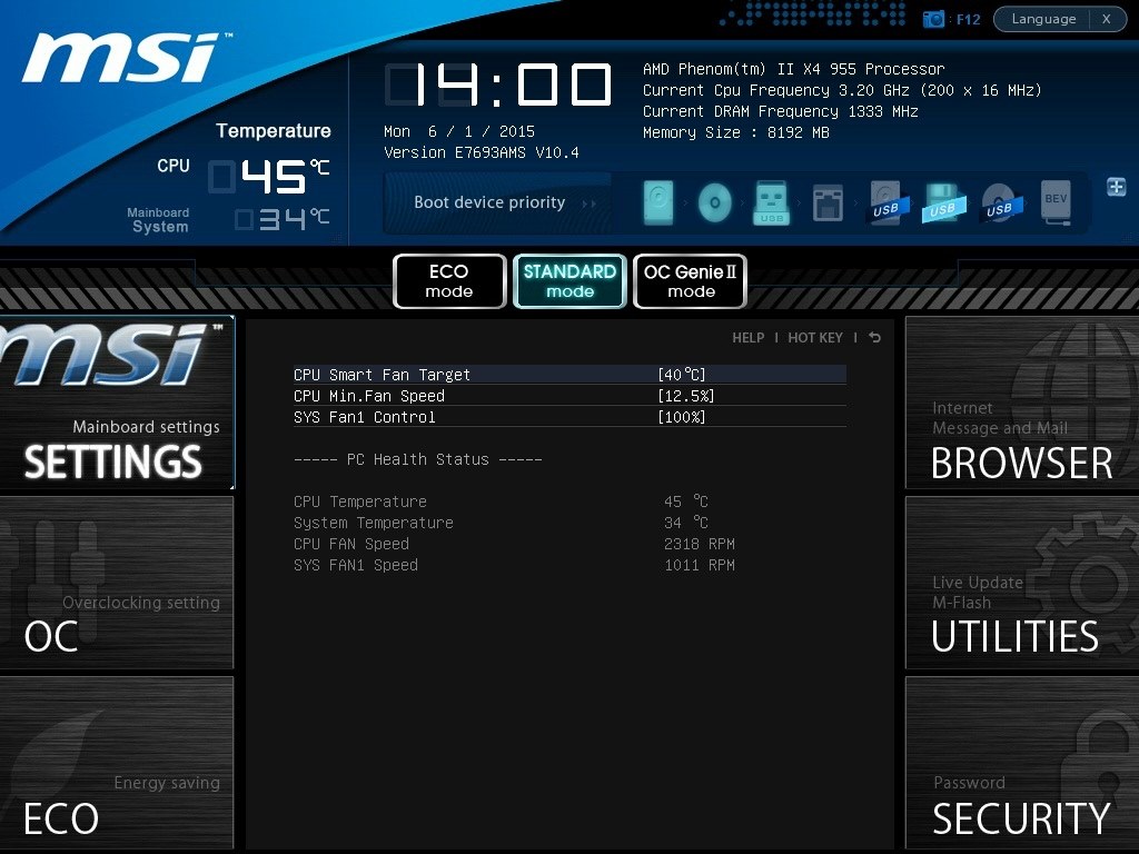 Initially, the line included models at 20, 25 and 33 MHz (later it was supplemented by models at 40 and 50 MHz). Users got the opportunity to overclock, which does not require soldering and replacing the crystal oscillator.
You could also achieve DX2-66 ($799) performance by purchasing a $400 486DX2-40 and increasing its standard bus speed from 20 MHz to 33 MHz.
Due to stability issues and the VLB slot, at bus speeds above 33 MHz, overclocking capability decreased as the base frequency increased; to the point that many Intel DX2-66s did not overclock at all, and some were often limited to only 80 megahertz (2 x 40 MHz).
Intel Celeron 300A
Release date: August 24, 1998
Standard clock: 300 MHz
Overclocking: 375 — 504 MHz (~55%)
Overclocking is believed to have gained immense popularity in the late 90s thanks to the ease of overclocking the legendary Celeron 300A. To overclock it by 50% to 450 MHz, it was enough just to change the bus speed from the nominal 66 MHz to 100 MHz. While some motherboards topped out at 83.3 MHz, limiting overclocking to 375 MHz, boards with 103 MHz system bus (FSB) support allowed 464 MHz.
The highest quality chips could operate at 112 MHz FSB when the voltage was increased, providing a processor frequency of 504 MHz. Notably, the 300A could typically reach 450MHz without additional voltage requirements, at the nominal 2.0V. The on-chip L2 cache also helped the chip’s performance, and at $149 it was especially handy for system builders.
AMD Athlon 700 (Thunderbird) / Duron 600 (Spitfire)
Release date: July 5, 2000 (Athlon 700) / June 19, 2000 (Duron 600)
Standard clock: 700 MHz/600 MHz
Overclock: 770 — 900 MHz (~12%) / 800 — 1000MHz (~59%)
The AMD Thunderbird «pencil» mod has become an overclocker’s dream come true. AMD has locked down the voltage and multipliers of the K7 line in an attempt to prevent fraudulent relabeling of processors. Overclockers quickly figured out that the key to unlocking performance was the board’s jumpers built into the case.
Initially, the combination of connection jumpers in blocks L3, L4 and L6 allowed shorting L1 connections to unlock the multiplier. It was also possible to close the connections of the L7 block to change the core voltage, and a soft graphite pencil or pen that applied conductive tracks was enough to carry out this process.
Because the AMD EV6 FSB was sensitive to overclocking, multiplier overclocking was only available in the Duron line due to its lower core voltage (1.5V instead of 1.7V/1.75V), which allowed for a larger relative boost to max. allowable 1.85 V.
At only $112, the Duron 600 could easily match the performance of a processor many times its price in a matter of minutes.
Intel Core 2 Quad Q6600 G0 Revision
Release date: January 8, 2007 (B0 revision) / July 22, 2007 (G0 revision)
Standard clock speed: 9001 7 2. 4 GHz
4 GHz
Overclocking : 3.4 — 3.6 GHz (~46%)
Core 2 Quad Q6600 achieved an enviable life and performance record, becoming the de facto choice for overclockers looking to purchase a budget quad-core CPU. Since January 2007, its original price ($851) has fallen rapidly, reaching $530 in May; further price restructuring in July coincided with the release of version G0. At $266, the 2.4GHz quad-core chip was as costly as the new dual-core 3GHz E6850, which could easily outperform the Q6600 of the earlier B3.
The new version of G0 provided slightly lower power consumption, resulting in improved overclocking capabilities. Thanks to this, many users were able to achieve stable 3.4 — 3.6 GHz almost effortlessly. The advent of the affordable Intel P35 platform and the further reduction in the price of the Q6600 throughout 2008 from $224 (in April) to $183 (in October) provided the possibility of reliable overclocking within 50% (a 9x multiplier and a 400 MHz system bus gave 3. 6 GHz ) at a reasonable cost. This model remained very competitive long after many modern processors fell out of favor.
Intel Pentium III 500E
Release date: October 25, 1999
Standard clock speed: 500 MHz
Overclocking: 667 — 775 MHz (~50%)
Coppermine overclocking reasons The Pentium III 500E and 550E had processor binning by Intel «overstock», a low system bus frequency (100 MHz) and an integrated L2 cache. Budget pricing ($239) and the ability to use older Slot 1 motherboards with Socket 370 to Slot 1 adapters provided remarkable performance at a modest cost.
500E could easily work at 667 MHz after selecting a system bus frequency of 133 MHz in the BIOS or after insulating the A14 contact of the Slocket adapter with electrical tape or varnish. On more expensive boards, it was possible to reach 750 MHz (FSB 150 MHz) and higher, getting the same performance as the $850 Pentium III 800.
However, there were some peculiarities during overclocking, for example, motherboards had to support AGP and PCI clock dividers (respectively, 1:2 and 1:4) to ensure the stability of installed components and fast PC133 RAM.
AMD Athlon XP-M 2500+ (Barton Mainstream 45W TDP)
Release Date: March 12, 2003
Standard Clock: 1.87 GHz 9000 3
Acceleration: 2.4 — 2.7 GHz (~32%)
In early 2004, the overclocking community took notice of the fact that Barton mobile processors had an unlocked clock multiplier; in addition, they are designed to operate at reduced voltage (1.45 V compared to desktop 1.65 V). These factors often provided phenomenal overclocking capabilities that were lacking in desktop models.
When the overclocking potential of this chip became known to the general public, its price rose from the original $75 by 30% in a matter of weeks. On a reliable nForce2 motherboard with good cooling, when the voltage was increased to 1. 8 V and higher, it was often possible to achieve overclocking up to 30-40%. While such impressive growth didn’t close the performance gap with the new Athlon 64s, the Athlon XP-M 2500+ still didn’t cost $200 to $400.
AMD Opteron 144 / 146 (K8 Venus)
Release Date: August 2, 2005
Standard Clock: 1.8GHz / 2.0GHz
Overclocking: 2.5 — 3.0 GHz (~63%)
Using the same silicon as San Diego’s Athlon 64 processors, the $125 and $183 Opterons for Socket 939 had a significant price advantage over the similarly-specified Athlon 64 3700+ ($329) and more. fared better against the $1,000 FX-57.
As with all CPUs locked from boost, the Opteron’s ability to overclock was directly related to the power of the chosen motherboard. Overclocked Opteron server chip binning combined with a solid overclocking board such as the nForce4 chipset and HyperTransport clocks reaching (and exceeding) 300MT/s allowed overclocking rarely achieved by enterprise-class processors.
While all Opteron models had approximately the same overclocking ceiling, the cheapest $144 chips were quickly sold out in many countries.
Intel Core i7 2600K / Core i5 2500K
Release date: January 9, 2011
Standard clock: 3.4GHz (Turbo 3.8GHz) / 3, 3 GHz (Turbo 3, 7 GHz)
Overclocking: 4.6 — 5.0 GHz (~49%)
Sandy Bridge, most users considered this the end of overclocking for Intel platforms. However, in fact, the 2500K and 2600K models turned out to be ideal for overclocking, allowing you to achieve stable overclocking by 30-50% with minimal time and improved cooling.
The popularity of the 2600K was such that overclocking results for this processor in 2011 accounted for 28% of all published on the HWBot website, and in 2012 they outnumbered its descendant, the 3770K. With its low price (only $216) plus good air or water cooling options, the Intel 2500K has become the de facto standard for evaluating all consumer-grade CPUs.
Intel Core i7 920
Release date: November 17, 2008
Standard clock: 2.67 GHz (Turbo 2.93 GHz)
Overclock: 3.5 — 4.0 GHz in C0 version, 3.8 — 4.2 GHz in D0 versions (~58%)
The new Nehalem architecture and X58 platform seemed attractive enough to attract many users of long-lived Core 2 LGA 775 systems. was still less relevant than the i7 920.
The first Bloomfield C0 processors required high voltages above 3.6 GHz, and the next D0 revision often had the ability to maintain the 1.26 V nominal voltage up to 4 GHz and reach an absolute overclocking ceiling of almost 4.5 GHz if the user tried increasing the voltage to 1.5 V.
The popularity of the 920 was (and still is) such that its overclocking reports account for a third of the total number of LGA 1366 results.
Intel Pentium 4 1.6A / Celeron 2.0 (Northwood)
Release date: January 7, 2002 (Pentium 4) / September 18, 2002 (Celeron 2. 0)
0)
Standard clock: 1.6 GHz / 2.0 GHz
Acceleration: 2 .4 — 2.8 GHz (~48%) / 2.66 — 3 GHz (~46%)
The arrival of the Northwood core was a welcome development after the disappointing Williamette, whose high voltage and heat dissipation prevented massive overclocking. While the overclocked P4s were of little value compared to the XP, the $125 1.6A model turned a performance deficit into a benefit with a low base system bus frequency (100MHz) that could easily be bumped up to 150MHz to get a speed of 2. 4 GHz.
The 20x Celeron overclocked was still better, although performance was severely limited by the modest 128 KB L2 cache. Those looking for more overclocking needed to raise the voltage above 1.6V either through the BIOS or with a wired mod (by connecting the CPU pins to raise the Vcore limit). The latter method was the main cause of the phenomenon called S.N.D.S. (Sudden Northwood Death Syndrome, Northwood Sudden Death Syndrome), better known as electrotransfer.
This, and the fact that the 1.6A hurt sales of Intel’s expensive models, led the company to stop selling the 1.6A just six months after it was released in January 2002.
Intel Xeon LV 1.6 D1 revision (Prestonia)
Release date: September 2003
Standard clock: 1.6 GHz
900 16 Overclocking: 2.6 — 3.2 GHz (~63%)
Most often, overclocking is associated with gaming systems, but for more than a decade, dual-processor overclocking has been very popular. Long before the QX9The 775 and the Intel Skulltrail board became synonymous with performance, with many fans hunting for the budget Xeon LV 1.6.
The Prestonia core was essentially a Pentium 4 Northwood processor that added SMP (symmetric multiprocessing) and HyperThreading as standard features. Although the $200 1.6GHz Xeon drew a promising 1.274V, overclockers usually couldn’t take advantage of the voltage boost option, since most boards had it blocked. However, by simply increasing the frequency of the system bus, 2.6 GHz could be obtained.
If the user was more adventurous, he could use three hardware mods and get overclocked to 100% (or even more!): U-Wire mod, which connected two (1.5 V) or three (1.6 C) a set of socket pins, a BSEL mod that isolates or breaks the CPU pins, while raising the FSB limit to 200 MHz, or a vDIMM mod that boosts the RAM voltage.
Those willing to push the limits of technology were rewarded with 3.2 GHz dual processor performance for about $700 (total cost of processors, coolers, board, and RAM).
AMD Athlon XP 1700+ (Thoroughbred-B)
Release Date: June 10, 2002
Standard Clock: 1.46 GHz
Overclock: 2.2 — 2.5 GHz (~44%)
The first Thoroughbred-A was almost the previous Palomino with a reduced die size and was rather disappointing as a finished product. Released in June 2002, AMD Thoroughbred-B was more adapted to the 130nm process, which resulted in higher core frequencies as well as increased efficiency, as version B showed remarkable overclocking capabilities with little or no boost.
Combined with a powerful motherboard based on the nForce2 chipset, the $60 XP 1700+ processor at standard voltage was able to achieve core speeds of almost 2 GHz. With an nF2 board capable of pushing the system bus above 200 MHz, it was possible to achieve a stable overclock of 40% at a moderate 1.7 V, which exceeded the performance of the $397 flagship AMD Athlon XP 2800+ and posed a threat to the Intel Pentium 4.
Intel Pentium D 820 / D 805
Release date: May 26, 2005 (D 820) / December 2005 (D 805)
Standard clock: 2.8 GHz / 2.66 GHz
Overclocking: 9002 6 3.5 — 4, 2 GHz (~26%)
The Pentium D 820 turned out to be a rather outstanding anomaly — two single cores in a multi-chip module package at a much lower price than the cheapest dual-core AMD Athlon 64 X2 ($241), even cheaper by $30, than the single core Athlon 64 3500+. The Pentium D 820 provided moderate performance that was by no means competitive with a dual Athlon, but had decent overclocking potential thanks to reasonable voltages and a good air or water cooling system.
The introduction of the Intel D 805 ($129) further drew the attention of budget overclockers to the hot Netburst processor. The decrease in the nominal system bus frequency from 200 to 133 MHz was compensated by the D 805 processor’s 20x multiplier, which kept overclocking interesting. For those on a budget, the D 805, when paired with a 945P board and appropriate RAM, provided the performance available in $500 processor builds.
Intel Pentium Dual Core E2140 / E2160
Release date: June 3, 2007
Standard clock: 1.6 GHz (E2140) / 1.8 GHz (E2160)
Overclocking: 900 17 2.7 — 3.2 GHz (~89%) / 2.9 — 3.5 GHz (~92%)
Intel’s E2000 series was both the death of the last surviving Pentium D with NetBurst and AMD’s dominance in the budget market. Intel has halved the L2 cache of the E4000 series and also slacked off the performance of the 200 MHz FSB (800 FSB). However, at the same time, Intel did not get rid of the overclocking capabilities of the Conroe processor.
At standard voltages and a conventional cooler, it was possible to achieve a 50% increase in clock speed by simply raising the 300 MHz bus speed, either on an inexpensive board with an Intel P965/P35, or on a board with an Nvidia 650i SLI chipset, which, due to the fact that it did not rely on on memory frequency dividers, provided more customization options.
A hand-bought air cooler, voltage regulation and a bit of luck in the silicon lottery were enough to overclock the processors by almost 100%, providing performance on par with the E6700 for a fraction of the price.
AMD Phenom II X2 550 Black Edition (Callisto) / X4 955 Black Edition (Deneb)
3
Standard clock speed: 3.1 GHz / 3.2 GHz
Overclocking: 3.7 — 3.9 GHz (~22%)
Release of the new version of the AMD K10.5 architecture in the first months of 2009 has become a symbol of the company’s strength in the niche of budget products. The arrival of Black Edition processors has also added a nice touch in the form of an unlocked multiplier for easier overclocking.
While the overall clock speed increase was not particularly impressive by historical standards, it went hand in hand with a real performance boost that lifted the processor out of the Core 2 Quad shadow. At $100, the 550 Black Edition was a huge value if it could unlock two disabled cores (unlocking the fourth core would be the X3 720 BE’s biggest selling point), and the $245 955 BE’s raw performance ensured that its potential could only be surpassed by a more expensive platform. X58.
Intel Core 2 Duo E6600 (Conroe)
Release Date: Jul 27, 2006
Standard Clock: 2.4 GHz
900 16 Overclock: 3.0 — 4.0 GHz (~45%)
At the time of release in July 2006, Intel Conroe focused on the unlocked X6800 multiplier, but the cheapest full-featured chip (4 MB L2 cache) played the most important role. At $316, the chip was $200 cheaper than the next highest performing chip (E6700) and delivered results that rivaled the most powerful AMD Athlon 64.
With standard cooling and voltage, the E6600 could be expected to reach 2.7-3 GHz. When buying a more powerful used cooler, motherboard stability was often the limiting factor, because system bus speeds exceeded 400 MHz and approached 450 MHz. The overclocking potential was so great that the prices of the X6800 ($999) and Athlon 64 FX-62 ($799) seemed obviously ridiculous when compared to the price and performance of the E6600.
Intel Core 2 Duo E8400 E0 Revision (Wolfdale-6M)
Release Date: January 7, 2008 (C0 Revision) / July 18, 2008 (E0 Revision)
Standard Clock Speed: 90 017 3.0GHz
Overclocked: 4.0 — 4.5 GHz (~41%)
Ever since the Wolfdale E8400’s C0 release in January 2008, it has immediately established itself as an affordable processor with performance upgrades. Five months later, the E0 version provided much more advanced voltage requirements. Some E8400s in the C0 version were capable of operating at 4 GHz, but in the new version, the same frequency could be achieved with standard voltage, parameters and a cooler.
By the time the E0 was released, OEM kit prices had dropped to $149, and various feature boards on the P45 and X48 were capable of supporting 500 MHz bus speeds (2000 MHz FSB). The stability of these systems at 4 GHz and above is a testament to the quality of both the architecture and the chipsets.
As advertised
Our company offers for rent servers with processors from Intel and AMD. In the latter case, these are epic servers! VDS with AMD EPYC, CPU core frequency up to 3.4 GHz. The maximum configuration is 128 CPU cores, 512 GB RAM, 4000 GB NVMe.
Xeon X5650 is the best processor for LGA 1366 socket
money.
Additional advantages include excellent overclocking potential and the ability to work with DDR3 ECC Reg.
Contents
- Xeon X5650 Specifications
- CPU-Z data
- Xeon X5650 overclocking and performance
- Xeon X5650 processor findings
Xeon X5650 specifications
| 9 0016 Options | Xeon X5650 |
| Cores/Threads | 6/12 |
| Base Clock | 2.66 GHz |
| Turbo Boost Max Clock | |
| L3 Cache | 12MB |
| TDP | 95W |
| Price | 850 RUB |
performance
Unfortunately, overclocking of this line of processors is not possible on Chinese and server motherboards. To overclock the processor to 4-4.5 GHz, you will need a well-known brand motherboard running on the X58 chipset. However, it is worth paying more attention to overclocking the memory controller and RAM, because without overclocking these components, you will not get a real effect in games and will experience low frames per second.
Buy LGA 1366 socket motherboards:
- Asus P6T Deluxe v2,
- Asus Sabertooth X58,
- Asus Rampage III.
Buy RAM:
- DDR3: First option, second option.
- DDR3 ECC reg: First option, second option.
Cooling: The snowman cooler (buy) proved to be the best.
You can watch a detailed video about the process of overclocking the processor below:
An example of performance with a GeForce 1080 video card with a Xeon X5650 overclocked to 3.8 GHz:
As you can see from the video, the processor can load even a card like the GeForce 1080 in this overclock, but modern games already have drawdowns and microfreezes.