Thermal Paste on CPU Pin? How to Remove Thermal Paste from CPU Socket? — Kooling Monster
Thermal paste knowledge
Written By Daniel Chen
Ideally, thermal paste and the underside of your CPU should never meet. And this isn’t a “star-crossed lovers” scenario – thermal paste should only ever be applied to the IHS (Integrated Heat Spreader) of your CPU where the heat is transferred over to the heatsink or waterblock. The underside of the CPU is more sensitive than the IHS. Things like moisture, oil from your fingers, and even an uncontrolled electrical current can cause harm to a chip if allowed onto the pins.
But things happen. Maybe you had some leftover thermal paste on your gloves or another component, maybe you were replacing your CPU, or maybe some thermal paste accidentally dripped down into the socket. Don’t worry, there’s no reason to panic… maybe. Keep reading to find out why.
What happens if you get thermal paste on the pins or socket?
This actually depends on what type of thermal paste you are using.
It is important to make sure whether the thermal paste is electrically conductive. You can usually find the information on the packaging or through a quick google search. If it is, then you may want to start looking for a new CPU after getting paste on the pins, or at the very least, consider that there might be some damage to your current one. At this point it would also be important to not come into contact with unnecessary electricity – that means doing the rest of this process grounded and preferably on top of a non-conductive material.
However, if your thermal paste is not electrically-conductive, you’re probably in the clear. Despite their sensitivity to substances, CPU pins can also be unusually resilient if handled in the right way. There is a straight-forward and easy process to clean them.
How to clean thermal paste from CPU pins?
There are generally two types of CPU sockets: Pinhole socket (PGA) and Pin Socket (LGA).
For Pinhole socket (PGA)
A toothbrush is very useful in this scenario. Assuming you’re using a PGA connector (like the ones AMD uses for most of their chips), you’ll need a toothbrush with soft bristles to be able to gently rub off the thermal paste without damaging the pins. You’ll also need a substance that isn’t conductive and won’t leave moisture on the chip after the process is finished. For this, we recommend isopropyl alcohol. The higher the quality, the better. Usually 99% is recommended as it would dry faster but anything over 91% will do the trick.
Your shopping list is:
· Soft bristle toothbrush
· Isopropyl alcohol (91% or higher)
· Paper towel
The process:
1. Pour a little bit of isopropyl alcohol into a cup or glass
2. Soak the toothbrush in it for up to a minute
3. VERY GENTLY scrape the thermal paste from the inside of the processor outwards
4. When the toothbrush gets dirty, wipe it off on the paper towel and add more alcohol
5. Once you think all of the thermal paste has been wiped off, let the CPU dry for 2 minutes
For Pin Socket (LGA)
However, if you’re working with an LGA connector like those that Intel uses, the process may be much easier. As LGA connectors don’t have pins on the underside of the CPU, you can simply use a paper towel with alcohol or a specialized wipe to gently wipe off the thermal paste.
We recommend the Kooling Monster KLEAN-01. It uses a specialized formula which effectively cleans thermal paste off of any surface – so you won’t need to bother yourself with what kind of alcohol to buy or how much to use.
What happens if you don’t clean thermal paste off CPU pins?
At this point you might be thinking “that’s all well and good, but do I really have to clean it? Can’t I use it as it?”
Answer: Yes, you do. And no, you can’t.
Let’s break this down. You may already know that the reason you apply the thermal paste to the top of your CPU (or the IHS) is because that’s the part that transfers heat. But what about the other side? That’s where the heat is initially coming from, but why does that happen and what’s so important about it?
Without going into deep detail, a CPU takes instructions from your input, processes them, and then spits out some sort of output. Hence the term “processor”. So if you tap on a key on your keyboard, the CPU receives the tap, processes it, and quickly spits out a letter on the screen. On the physical level, what this involves is getting the electrical signal or the “input” into your CPU.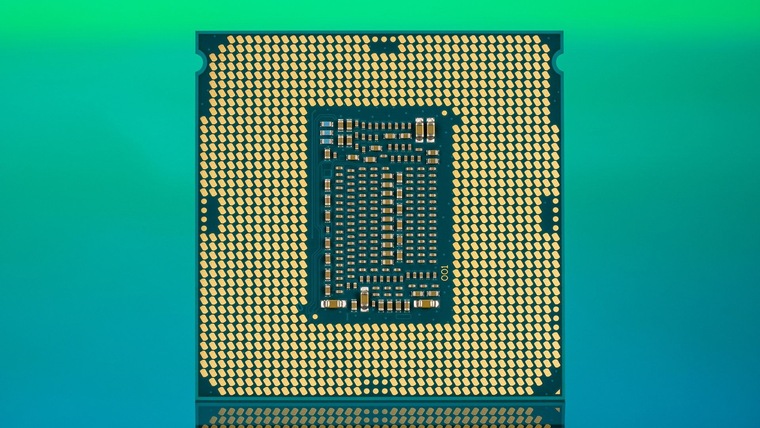 How? You guessed it: through the pins.
(Though, realistically, this involves billions of signals going in and coming out which is where the heat is generated.)
There are generally 3 kinds of pins in a CPU: Address Pins, which transmit address values (i.e. the “location” of your keyboard, mouse, microphone, etc.), Data Pins, which receive data (i.e. you pressing a button), and Control Pins which do a bunch of stuff mostly to do with… well… control. No matter what the pin type is, it requires a clean an unobstructed space to communicate with the rest of the components and do its job.
As we’ve discussed before, lots of substances can interfere with pin function like oil or moisture. Or, in our case right now: thermal paste. By not removing thermal paste from your pins, you are effectively obstructing your computer’s processing power. Depending on which types of pins are blocked, your PC might not even boot up at all.
So yes, cleaning the thermal paste off is a must. It is also important to clean the thermal paste from the CPU – keep reading to find out how.
How to clean thermal paste off CPU
We touched upon this process in our Beginner’s Guide, but as a short reminder, here’s the process:
Here are some reminders:
-
Take off the cooler (this can be your stock heatsink, your aircooling heatsink, or if you’re using watercooling it would be the waterblock)
-
Use an alcohol + cotton swab + paper towel combo to clean the old thermal paste off your CPU and heatsink
***or just make your life easier and use the Kooling Monster KLEAN-01 cleaning wipe and gloves – the wipe is made with a special formula to remove the driest thermal paste without leaving any lint to clean up and the gloves protect your hands from the chemicals.
-
Wait 2 minutes for the surfaces to dry
-
Use any of the patterns mentioned above and apply the thermal paste onto the CPU ONLY (we recommend the cross or the buttered toast)
-
Reinstall your heatsink by carefully placing it on top of the CPU and tightening the screws
-
Check the area around where the CPU and heatsink meet for any spillage and use a paper towel (or our specialty wipes) to clean it up
Daniel Chen
How to install a CPU
Now that Intel’s 12th Gen Alder Lake processors have arrived, it seems like an opportune time for a refresher on how to install a CPU.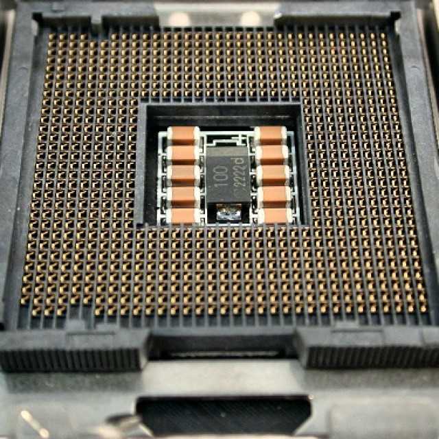 And yes, AMD, you can come too.
Whether go the Core or Ryzen route – our best CPU for gaming list has our recommendations – this guide will cover how to secure your chip in its motherboard socket, how to apply thermal paste without drowning it, and tips for installing a cooler. The photos here are all of Intel’s LGA sockets, but I’ve included instructions for installing AMD CPUs as well.
Watch on YouTube
This is also one in a series of guides which I’m hoping will both help and encourage you to make your own PC upgrades, if you haven’t before. Some of them, like how to install RAM and how to install an SSD, can be enacted in mere minutes, and can produce serious performance improvements to your personalised rig. Installing a gleaming new CPU will have an even greater effect on games performance, so simply follow the steps below to give your PC a brand new brain.
Intel LGA 1151 and LGA 1200 sockets look similar, but only fit certain CPU models.
How to install a CPU in the motherboard
Before you even buy a new CPU, make sure you’re matching it with a compatible motherboard. AMD Ryzen chips usually share the AM4 socket design, but recent models will recent chipsets as well. Intel, meanwhile, introduce new chipsets with every generation, and change sockets much more frequently than AMD, so don’t expect much backwards compatibility. That said, the physical process of slotting an Intel chip into its socket remains consistent.
Regardless of your hardware choices, you’ll find this whole process a lot easier if you do it outside of your PC’s case. If you’re adding a new chip to a previously installed motherboard, take out the mobo first.
Step 1: For Intel CPUs, push down on the metal arm next to the socket, pull it slightly away from the socket, then lift it up. This will let you lift up the metal frame covering the empty socket.
If you’re using a brand new mobo, don’t forget to remove the black plastic socket cover.
On Intel LGA 1700 socket like this one, the cover hinge is at the bottom of the socket, but is otherwise similar enough to top-hinged LGA 1200 and 1151 sockets.
For AMD CPUs, simply lift up the socket’s metal arm as far as it will go. You’ll see the socket slide sideways a little.
Step 2: For Intel CPUs, simply plop the processor into the slot. If you’re unsure of how to orient it, look for little notches in the side of the chip that align with tiny protusions in the socket. Once correctly inserted, it should lay down perfectly flat.
See those teensy little notches near the top of the chip?
For AMD CPUs, hold the processor so that the pins on the underside are aligned with the holes in the socket. Lower it down into the socket until it rests completely flush – there shouldn’t be any gap between the chip and the top of the socket. If there is, pull the CPU out and try again.
Step 3: For Intel CPUs, lower the metal frame over the inserted chip and back into its starting position.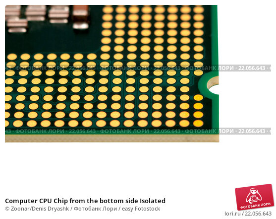 Press the metal arm back down, then tuck it under the catch. This will lock the frame in place, securing the CPU in turn.
On Intel sockets, this is basically step 1 in reverse.
For AMD CPUs, simply press the metal arm down. This will slide both the socket and the inserted Ryzen chip into the former’s original position, locking both in place.
Not particularly blob-shaped, but that’s the right amount for this particular CPU.
How to apply thermal paste
Thermal paste, thermal grease, thermal compound, sticky grey heat transfer goop – whatever you call it, it pays to know to apply it. Even if a lot of CPU coolers come with some pre-applied paste, different CPUs come in different sizes, and the best way to make sure you’re applying the right amount is to do it yourself.
But what is the right amount? Ideally you want a very thin, even layer covering the entire IHS (integrated heat spreader, the metallic top ‘layer’ of the CPU that makes contact with the cooler).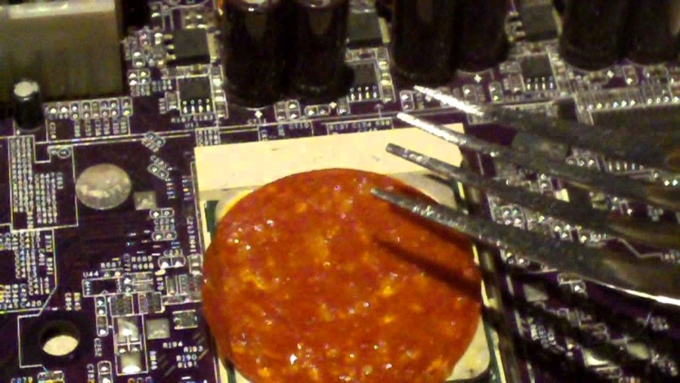 On Intel chips that fit in LGA 1151 or LGA 1200 sockets, that amounts to about a pea-sized blob, while AMD’s bigger Ryzen chips need a slightly-bigger-than-pea-sized blob. Alder Lake/LGA 1700 processors are taller than 10th and 11th Gen Intel chips, so could also use a tiny bit extra.
I personally like to just eyeball the amount, drop it right in the middle of the chip, and install the cooler immediately. The cooler’s contact plate pressing down on the paste will, if the weight is applied evenly, produce a nice, level spread without any extra tools. However, if you want to be absolutely sure you’re covering the whole IHS, you can instead use a piece of card or comically small plastic spatula to spread the paste around before installing the cooler on top. This also lets you scoop up any excess paste; remember we only want a thin layer, as having too much will insulate the processor instead of facilitating heat transfer.
Manual spreading isn’t strictly necessary, but guarantees no unpasted spots.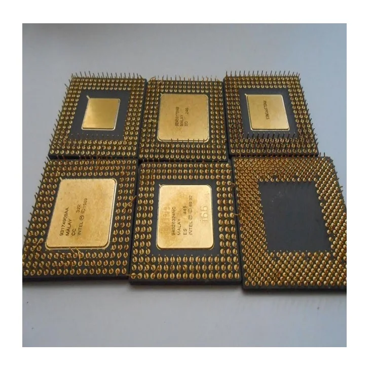
Coolers that don’t come with pre-applied paste may instead include a little tube of it in the box, though it’s not expensive to buy. A 4g tube of Arctic MX-5 costs £6 / $7, and is enough for several applications.
Tighten thumbscrews with, uh, thumbs. Then secure them fully with ascrewdriver.
How to install a CPU cooler
Please forgive the lack of true guide-yness in this section, as there’s no single methodology for installing a CPU cooler: not only are there different types of water and air coolers, but manufacturers use distinct mounting methods and kits. I’m planning a more detailed guide on how to install AIO watercoolers for the future, but generally you’re best off following the printed installation instructions for your specific cooler model.
That said, I do have some tips that apply to a majority of air coolers and AIO watercoolers…
- Assemble everything outside your PC. As much as you can, anyway – if you have an AIO cooler and want to position the fans between the case and the radiator, you usually need to yoke all three together at once with long screws.
 Otherwise, it’s much easier to get everything put together on a table than in a darkened metal box.
 - When bringing the cooler down on top of the CPU, make sure to apply level pressure, so you’re not smooshing the thermal paste unevenly. If your cooler attaches to the socket with thumbscrews, it might also help if you get all of them partially tightened before you fully tighten them – if you go from 0 to 100 on each screw at a time, that applies uneven pressure as well.
- If, for whatever reason, you remove the cooler after already making contact with the pasted-up CPU, clean off any thermal paste from both the chip and the cooler and re-apply it. This sounds wasteful but the distressed texture of the used paste makes it unlikely to re-acquire an even layer.
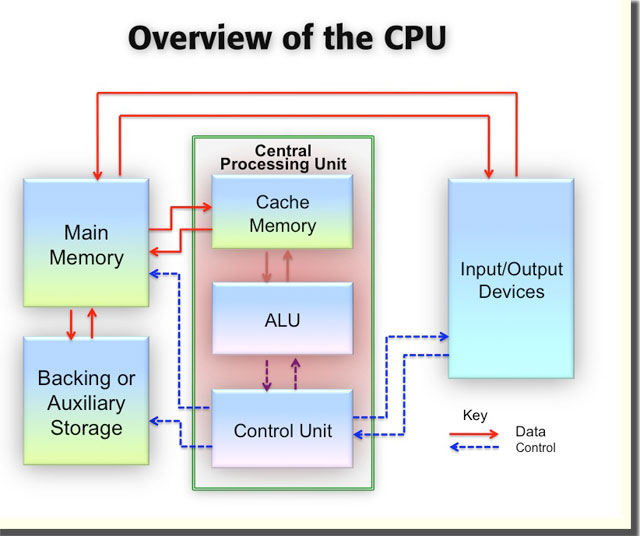
How processors work: A look from the outside | PC World
HOW CPUS WORK: A CLOSER LOOK AT EXTERIOR PROCESSOR DESIGN, PCWorld May 2016.
Processors are located at the heart of the computer. They execute millions of instructions every second, making it possible to watch Netflix or play Fallout 4. They lower their clock speed to save power and increase it when you need to open a new tab in Chrome. But have you ever paid attention to what a processor actually looks like? nine0009 Recent breakdowns of computers with Skylake processors have clearly demonstrated that the physical features of the chip play a more significant role than one might think. So let’s take a closer look at the Intel Core i7-4790K and AMD’s FX-8370 models.
Don’t Forget the Triangle
Anyone who has ever built a PC will attest to the fact that you need to be very careful and careful when installing a processor into its intended socket, especially if you are doing it for the first time. Intel (and AMD) processors give you a hint: align the triangle on the corner of the chip with the corresponding triangle on the edge of the processor socket. nine0007
Despite the triangular help, the lever that secures the processor may seem to be pushing too hard.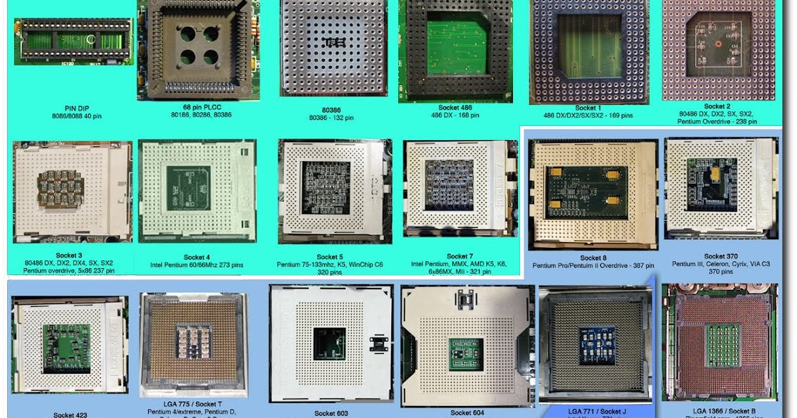 In fact, this is not so.
Pads
There are hundreds of small electrical contacts on the bottom of modern Intel processors. Each one contacts a small pin on the Land Grid Array socket, allowing the processor to draw power from the motherboard and communicate with the rest of the system. nine0007
Staggered design
The appearance of Intel processors is formed by a metal heatsink and a small printed circuit board. They are slightly offset from each other, forming two independent areas, and the heat sink has a stepped design. A hinged cover is pressed against its lower part, holding the processor in the socket, and a heat sink is pressed against its upper part, which removes heat. These two components do not touch each other.
Symmetrically placed small notches, along with the already mentioned triangle, will help to correctly insert the processor into the socket. nine0007
Test pads
The top edge of the Intel processor board has pads that look similar to the pins on the bottom edge.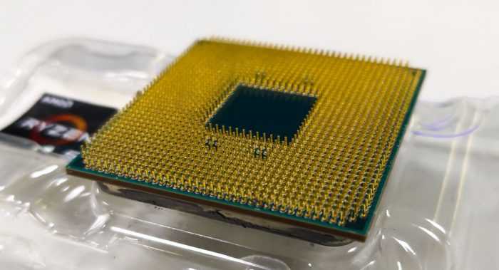 These test sites are used in the course of fine-tuning and debugging of processors. In addition, they are designed to test and sort processors at the factory before they are sent to customers. During the testing process, the correct functioning of the chip is checked, and the sorting procedure allows you to find out at what frequency, in accordance with the classification defined for a particular model, the processor operates stably. nine0007
Bottom view
At the bottom of the Intel processor, in addition to the pads, there is a central power supply circuit with capacitors. The Intel Core i7-4790K has more capacitors than the i7-4770K for smoother voltage regulation when overclocking.
AMD Product Differences
AMD processors do not have pads and power supply circuitry at the bottom. Whereas the Intel LGA design provides for the placement of pins in the motherboard connector, the AMD Pin Grid Array package contains a dense array of processor pins that form the electrical connections between the processor and the motherboard.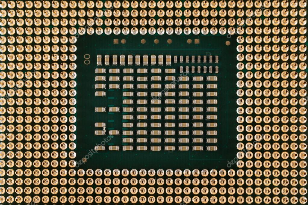 nine0009 The AMD FX-8370 processor installed in the AMD AM3+ socket has over 900 pins on the bottom.
Pins, pins
Since AMD processors have pins, one awkward move can cause some of them to bend. (In contrast, Intel processors can be installed with little or no risk.) Luckily, bent legs can be straightened out with a credit card to straighten them into position.
Flat surface
AMD sockets do not have a cover that presses the processor, and therefore the chips themselves have not a stepped, but actually a flat design. There is a small lever on the side of the connector. It presses the pins of the processor to the contacts of the motherboard and keeps them in a stationary state under the influence of friction.
The surface of the heatsink is placed on a large heat sink covering the silicon die of the processor.
Triangle 9 again0006
AMD and Intel processors have one important thing in common.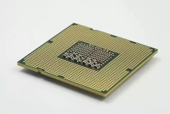 AMD chips are also marked with a small triangle, which helps to correctly orient the processor in the socket. A small triangle marks both the top and bottom faces of the chip. A corresponding marker is also available on all motherboards designed to install AMD processors.
Under the hood … more precisely, under the heatsink
Another common feature of Intel and AMD processors is the presence of a silicon crystal located inside the processor, in the center of its case, which has just been considered. (The figure shows a substrate that combines many, many Intel Haswell processor chips.)
Roughly the length of a pin, these tiny integrated circuits allow a computer to calculate the trajectory of enemies in a game or stream Twitch video with your friend making a sandwich. No matter how you use your PC, the technology behind it is on the verge of magic.
And that’s not all!
Interested in a deeper dive into the hardware that makes up a PC? Especially for this, we chopped the RAM into small pieces and tore the motherboard to shreds to show how the corresponding components work.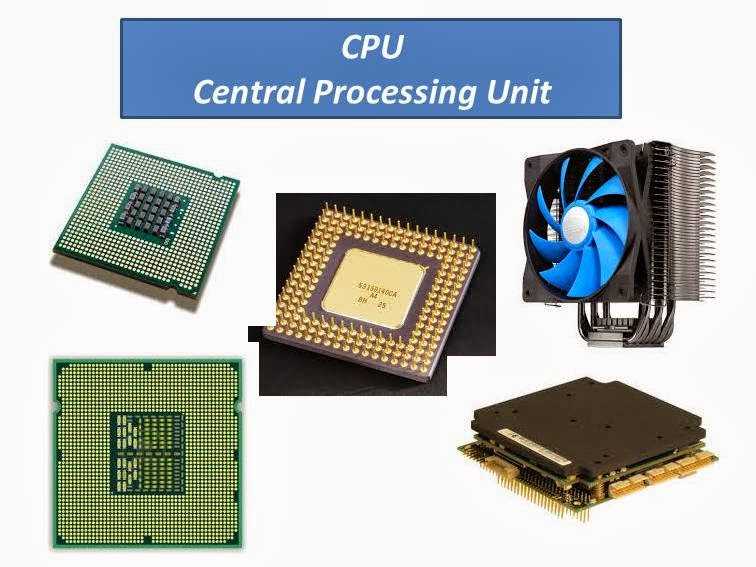 More on that in the following issues. Don’t pass by! nine0007
From sand to processor / Sudo Null IT News
It’s hard to believe, but a modern processor is the most complex finished product on Earth — and after all, it would seem, what is so complicated about this piece of iron?
As promised — a detailed story about how processors are made … starting with sand. Everything you wanted to know but were afraid to ask )
I have already talked about “ Where processors are manufactured” and about what “ Production difficulties » stand in this way. Today we will talk directly about the production itself — «from and to».
Processor manufacturing
When a factory for the production of processors using a new technology is built, it has 4 years to recoup the investment (over $5 billion) and make a profit. From simple secret calculations, it turns out that the factory should produce at least 100 working plates per hour.![]()
Briefly, the process of manufacturing a processor looks like this: a single crystal of a cylindrical shape is grown from molten silicon using special equipment. The resulting ingot is cooled and cut into «pancakes», the surface of which is carefully leveled and polished to a mirror finish. Then, in the «clean rooms» of semiconductor factories, integrated circuits are created on silicon wafers by photolithography and etching. After re-cleaning the wafers, laboratory specialists perform selective testing of processors under a microscope — if everything is OK, then the finished wafers are cut into separate processors, which are later enclosed in cases. nine0007
Chemistry lessons
Let’s look at the whole process in more detail. The content of silicon in the earth’s crust is about 25-30% by weight, due to which this element ranks second in abundance after oxygen. Sand, especially quartz, has a high percentage of silicon in the form of silicon dioxide (SiO 2 ) and at the beginning of the production process is the basic component for creating semiconductors.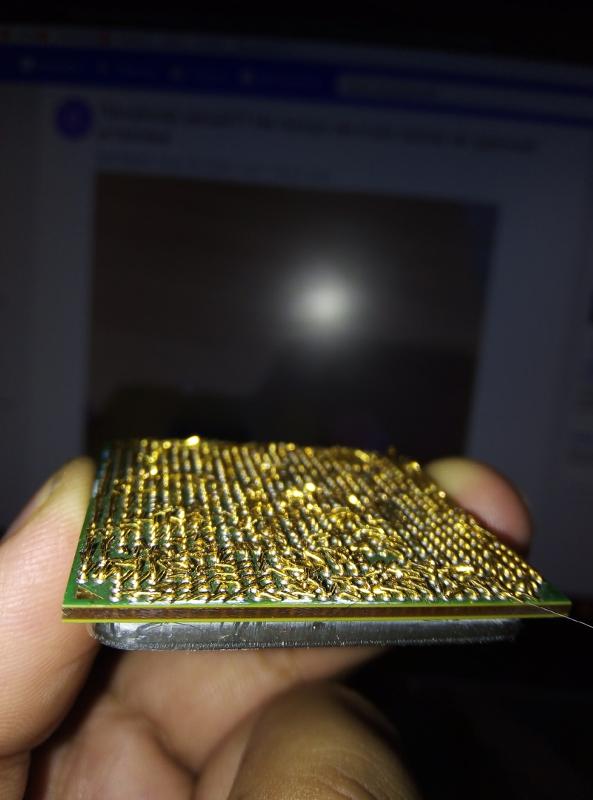
Initially SiO 9 is taken0105 2 in the form of sand, which is reduced with coke in arc furnaces (at about 1800°C):
SiO 2 + 2C = Si + 2CO
-99.9%. The production of processors requires a much cleaner raw material, called « electronic silicon » — this should have no more than one foreign atom per billion silicon atoms. To be refined to this level, silicon is literally «born again». Silicon tetrachloride (SiCl 4 ), which is subsequently converted into trichlorsilan (SIHCL 3 ):
3SICL 4 + 2H 2 + SI ↔ 4SIHCL
These reactions using the recocry of the recesses using the recocry of the recesses using the recesses of the recesses using the recesses. eliminate environmental problems:
2SiHCl 3 ↔ SiH 2 Cl 2 + SiCl 4
2SiH 2 Cl 2 ↔ SiH 3 Cl + SiHCl 3
2SiH 3 Cl ↔ SiH 4 + SiH 2 Cl 2
SiH 4 ↔ Si + 2H 2
The resulting hydrogen can be used in many places, but the most important thing is that “electronic” silicon was obtained, pure-pure (99.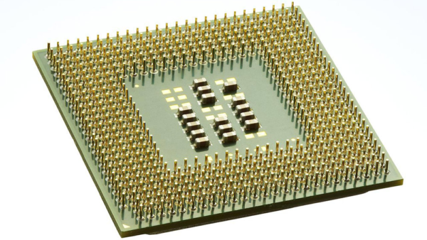 9999999%). A little later, a seed (“growth point”) is lowered into the melt of such silicon, which is gradually drawn out of the crucible. As a result, the so-called «boule» is formed — a single crystal as high as an adult. The weight is appropriate — in production, such a muzzle weighs about 100 kg. nine0007
The ingot is skinned with “zero” 🙂 and cut with a diamond saw. The output is wafers (codenamed «wafer») with a thickness of about 1 mm and a diameter of 300 mm (~12 inches; these are the ones used for the 32nm process technology with HKMG, High-K / Metal Gate technology). Once upon a time, Intel used disks with a diameter of 50mm (2″), and in the near future it is already planned to switch to wafers with a diameter of 450mm — this is justified at least in terms of reducing the cost of manufacturing chips. Speaking of savings — all these crystals are grown outside of Intel, for processor manufacturing they are sourced elsewhere.0007
Each plate is polished, made perfectly smooth, bringing its surface to a mirror finish.
Chip production consists of more than three hundred operations, as a result of which more than 20 layers form a complex three-dimensional structure — the volume of the article available on Habré will not allow us to briefly talk about even half of this list 🙂 Therefore, very briefly and only about the most important stages.
So. It is necessary to transfer the structure of the future processor into polished silicon wafers, that is, to introduce impurities into certain parts of the silicon wafer, which eventually form transistors. How to do it? In general, applying various layers to a processor substrate is a whole science, because even in theory such a process is not easy (not to mention practice, taking into account the scale) … but it’s so nice to understand the complex;) Well, or at least try to figure it out. nine0007
Photolithography
The problem is solved using photolithography technology — the process of selective etching of the surface layer using a protective photomask. The technology is built on the principle of «light-pattern-photoresist» and proceeds as follows:
— A layer of material is applied to the silicon substrate, from which a pattern must be formed. photoresist is applied to it — a layer of photosensitive polymer material that changes its physical and chemical properties when irradiated with light. nine0009
— exposure is made (illumination of the photo layer for a precisely set period of time) through the photo mask
— Removal of spent photoresist.
The desired structure is drawn on a photomask, usually a plate of optical glass, on which opaque areas are applied photographically. Each such template contains one of the layers of the future processor, so it must be very accurate and practical.
Sometimes it is simply impossible to deposit certain materials in the right places of the plate, so it is much easier to apply the material to the entire surface at once, removing the excess from those places where it is not needed — the image above shows the application of photoresist in blue.
The wafer is irradiated with a stream of ions (positively or negatively charged atoms), which penetrate under the wafer surface at specified places and change the conductive properties of silicon (green areas are embedded foreign atoms). nine0007
How to isolate areas that do not require post-treatment? Before lithography, a protective dielectric film is applied to the surface of a silicon wafer (at a high temperature in a special chamber) — as I already said, instead of traditional silicon dioxide, Intel began to use High-K dielectric. It is thicker than silicon dioxide, but at the same time it has the same capacitive properties. Moreover, due to the increase in thickness, the leakage current through the dielectric is reduced, and as a result, it has become possible to obtain more energy-efficient processors. In general, it is much more difficult to ensure the uniformity of this film over the entire surface of the plate — in this regard, high-precision temperature control is used in production. nine0007
So. In those places that will be treated with impurities, the protective film is not needed — it is carefully removed by etching (removal of layer areas to form a multilayer structure with certain properties). And how to remove it not everywhere, but only in the right areas? To do this, another layer of photoresist must be applied over the film — due to the centrifugal force of the rotating plate, it is applied in a very thin layer.
In photography, light passes through the negative film, strikes the surface of the photographic paper, and changes its chemical properties. In photolithography, the principle is similar: light is passed through a photomask onto a photoresist, and in those places where it passed through the mask, individual sections of the photoresist change properties. Light radiation is passed through the masks, which is focused on the substrate. Accurate focusing requires a special system of lenses or mirrors that can not only reduce the image cut on the mask to the size of a chip, but also accurately project it on the workpiece.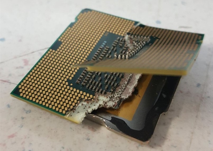 The printed plates are typically four times smaller than the masks themselves. nine0007
All spent photoresist (which has changed its solubility under the action of irradiation) is removed with a special chemical solution — along with it, part of the substrate under the exposed photoresist is dissolved. The part of the substrate that was covered from light by the mask will not dissolve. It forms a conductor or a future active element — the result of this approach is different patterns of short circuits on each layer of the microprocessor.
Strictly speaking, all the previous steps were needed in order to create semiconductor structures in the required places by introducing a donor (n-type) or acceptor (p-type) impurity. Suppose we need to make a p-type carrier concentration region in silicon, that is, a hole conduction band. To do this, the plate is processed using a device called Implanter — boron ions are fired with great energy from a high-voltage accelerator and are evenly distributed in unprotected zones formed during photolithography.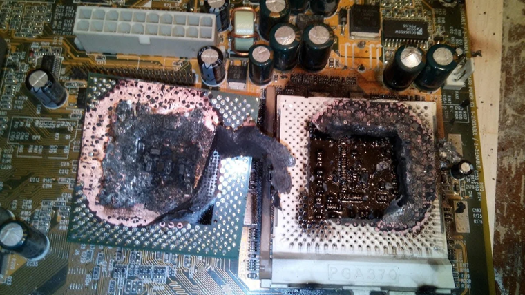
Where the dielectric has been removed, the ions penetrate the unprotected silicon layer — otherwise they get stuck in the dielectric. After the next etching process, the remnants of the dielectric are removed, and zones remain on the plate in which there is local boron. It is clear that modern processors can have several such layers — in this case, a dielectric layer is grown again in the resulting figure, and then everything goes along the trodden path — another layer of photoresist, the photolithography process (already using a new mask), etching, implantation … well, you understood. nine0007
The characteristic size of the transistor is now 32 nm, and the wavelength that silicon is processed is not even ordinary light, but a special ultraviolet excimer laser — 193 nm. However, the laws of optics do not allow resolution of two objects that are less than half a wavelength apart. This is due to the diffraction of light. How to be? Apply various tricks — for example, in addition to the mentioned excimer lasers that shine far in the ultraviolet spectrum, modern photolithography uses multilayer reflective optics using special masks and a special process of immersion (immersion) photolithography.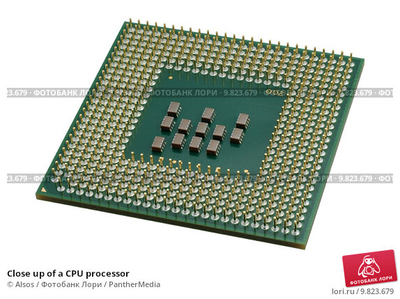 nine0007
Logic elements that are formed during the photolithography process must be connected to each other. To do this, the plates are placed in a solution of copper sulfate, in which, under the influence of an electric current, the metal atoms «settle» in the remaining «passages» — as a result of this galvanic process, conductive regions are formed that create connections between the individual parts of the processor «logic». Excess conductive coating is removed by polishing.
Finish line
Hooray — the hardest part is behind us. It remains a tricky way to connect the «remains» of transistors — the principle and sequence of all these connections (buses) is called the processor architecture. For each processor, these connections are different — although the circuits seem completely flat, in some cases up to 30 levels of such «wires» can be used. Remotely (at a very high magnification), all this looks like a futuristic road junction — and after all, someone is designing these balls! nine0007
When the wafer processing is completed, the wafers are transferred from production to the assembly and test shop. There, the crystals are first tested, and those that pass the test (and this is the vast majority) are cut out of the substrate with a special device.
At the next stage, the processor is packaged in a substrate (in the figure — an Intel Core i5 processor, consisting of a CPU and an HD graphics chip).
Hello socket!
The substrate, die, and heat-distributing cover are connected together — this is the product we will mean when we say the word «processor». The green substrate creates an electrical and mechanical interface (gold is used to electrically connect the silicon chip to the case), thanks to which it will be possible to install the processor in the motherboard socket — in fact, this is just a platform on which the contacts from the small chip are separated. The heat-distributing cover is a thermal interface that cools the processor during operation — it is to this cover that the cooling system will adjoin, whether it be a cooler radiator or a healthy water block.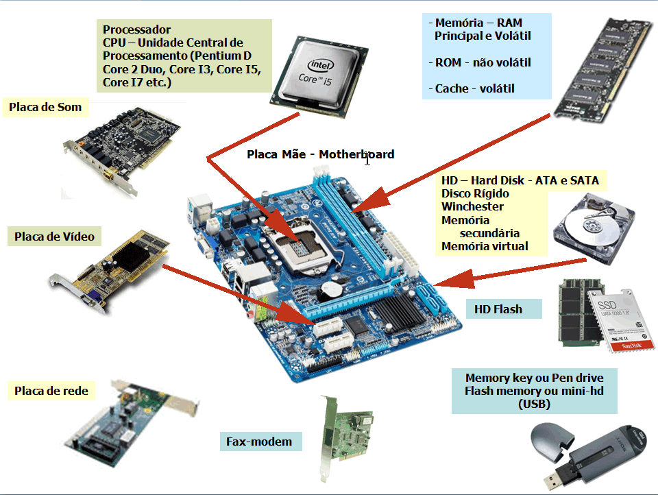 nine0007
Socket (CPU socket) is a female or slotted socket designed to install the CPU. Using a socket instead of directly soldering the processor on the motherboard makes it easier to replace the processor for computer upgrades or repairs. The connector can be designed to install the actual processor or CPU card (for example, in Pegasos). Each slot allows only a certain type of processor or CPU card to be installed. nine0007
At the final stage of production, finished processors undergo final tests for compliance with the main characteristics — if everything is in order, then the processors are sorted in the right order into special trays — in this form, the processors will go to manufacturers or go to OEM sales. Another batch will go on sale in the form of BOX versions — in a beautiful box along with a stock cooling system.
The end
Now imagine that a company announces, for example, 20 new processors.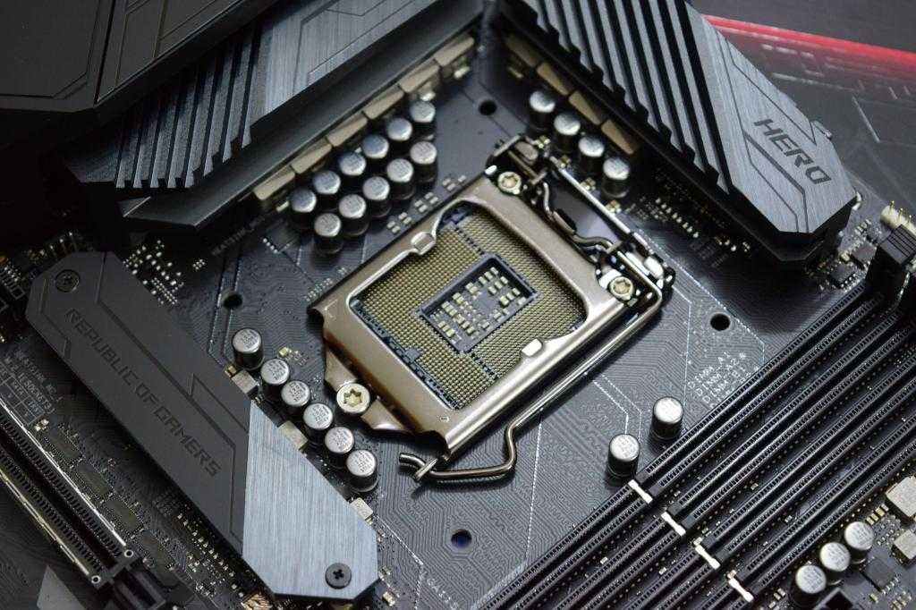 All of them are different from each other — the number of cores, cache volumes, supported technologies … Each processor model uses a certain number of transistors (calculated in millions and even billions), its own principle of connecting elements … And all this needs to be designed and created / automated — templates, lenses, lithographs, hundreds of parameters for each process, testing… And all this should work around the clock, in several factories at once… As a result, devices should appear that have no right to make mistakes in operation… And the cost of these technological masterpieces should be within the bounds of decency… I’m almost sure is that you, like me, also cannot imagine the whole amount of work being done, which I tried to talk about today. nine0007
And something even more amazing. Imagine that you are a great scientist without five minutes — carefully removed the heat-distributing cover of the processor and could see the structure of the processor through a huge microscope — all these connections, transistors .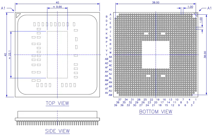 .. even sketched something on a piece of paper so as not to forget. Do you think it is easy to learn the principles of the processor, having only this data and data on what tasks can be solved with the help of this processor? It seems to me that such a picture is now visible to scientists who are trying to study the work of the human brain at a similar level. Only if the Stanford microbiologists are to be believed, there are more “transistors” in one human brain than in the entire global IT infrastructure. Interesting, right? nine0007
BONUS
Enough strength to read up to this paragraph? ) Congratulations — it’s nice that I tried not in vain. Then I propose to lean back and watch everything described above, but in the form of a more visual video — without it, the article would not be complete.
I wrote this article myself, trying to understand the intricacies of the processor building process. I mean, there may be some inaccuracies or errors in the article — if you find something, let me know.