Intel Launches 10nm ‘Ice Lake’ Datacenter CPU with Up to 40 Cores
The wait is over. Today Intel officially launched its 10nm datacenter CPU, the third-generation Intel Xeon Scalable processor, codenamed Ice Lake. With up to 40 “Sunny Cove” cores per processor, built-in acceleration and new instructions, the Ice Lake-SP platform offers a significant performance boost for AI, HPC, networking and cloud workloads, according to Intel.
In addition to increasing the core count from 28 to 40 over previous-gen Cascade Lake, Ice Lake provides eight channels of DDR4-3200 memory per socket and up to 64 lanes of PCIe Gen4 per socket, compared to six channels of DDR4-2933 and up to 48 lanes of PCI Gen3 per socket for the previous generation.
With these enhancements, along with AVX-512 for compute acceleration and DL Boost for AI acceleration, Ice Lake delivers an average 46 percent performance improvement for datacenter workloads and 53 higher average HPC performance, generation-over-generation, according to Intel. In early internal benchmarking*, Intel also showed Ice Lake outperforming the recently launched AMD third-generation Epyc processor, codenamed Milan, on key HPC, AI and cloud applications.
Intel’s Trish Damkroger
In an interview with HPCwire, Intel’s Vice President and General Manager of HPC Trish Damkroger highlighted the work that went into the Sunny Cove core as well as the HPC platform enhancements. “Having eight memory channels is key for memory bound workloads, and with the 40 cores along with AVX-512, the CPU shows great performance for a lot of workloads that are more compute bound,” she said. Damkroger further emphasized Intel’s Speed Select Technology (SST), which enables granular control over processor frequency, core count, and power. Although Speed Select was introduced on Cascade Lake, it previously only facilitated the configuring of frequency, but with Ice Lake, there is the added flexibility to dynamically adjust core count and power.
Using Intel’s Optane Persistent Memory (PMem) 200 series combined with traditional DRAM, the new Ice Lake processors support up to 6 terabytes of system memory per socket (versus 4.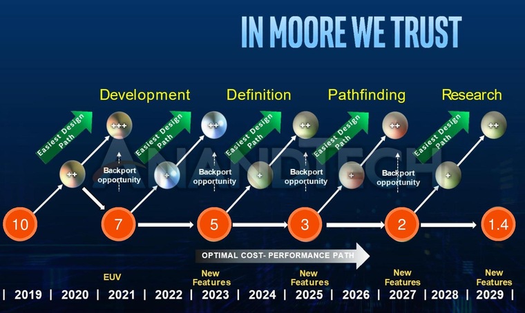 5 terabytes supported by Cascade Lake and Cascade Lake-Refresh). Optane PMem 200 is part of Intel’s datacenter portfolio targeting the new third-generation Xeon platform, along with Optane P5800X SSD, SSD D5-P5316 NAND, Intel Ethernet 800 series network adapters (offering up to 200GbE per PCIe 4.0 slot), and the company’s Agilex FPGAs.
In addition to moving to PCIe Gen4, which provides a 2X bandwidth increase compared with Gen3, the socket to socket interconnect rates for Ice Lake have increased nearly 7.7 percent for improved bandwidth between processors.
Gen over gen, Ice Lake delivers a 20 percent IPC improvement (28-core, ISO frequency, ISO compiler) and improved per-core performance on a range of workloads, shown on the slide below (comparing the 8380 to the 8280).
The combination of AVX-512 instructions (first implemented on the now-discontinued Intel Knights Landing Phi in 2016 and on Skylake in 2017) and the 8-channels of DDR4-3200 memory are proving especially valuable for boosting HPC workloads. With AVX-512 enabled, the 40-core, top-bin 8380 Platinum Xeon achieves 62 percent better performance on Linpack, over AVX2.
Compared with the previous-gen Cascade Lake, the Ice Lake 8380 Xeon achieves 38 percent higher performance on Linpack, 41 percent higher performance on HPCG, and 47 percent faster performance on Stream Triad, in Intel testing.
These improvements on industry-standard benchmarking apps are reflected on application codes used in earth system modeling, financial services, manufacturing, as well as life and material science. The slide below shows improvements on a total of 12 HPC applications, including 58 percent higher performance on the weather forecasting code WRF, 70 percent improved performance on Monte Carlo, 51 percent speed-up on OpenFoam, and 57 percent improvement on NAMD.
Damkroger said that the 57 percent improvement on NAMD — a molecular dynamics code used in life sciences — is just the start. Intel worked with the NAMD team at the University of Illinois Urbana-Champaign to further optimize performance, achieving a 2. 43X gen-over-gen performance boost (143 percent). “It’s all because of AVX-512 optimizations,” said Damkroger.
Source: Intel
At the University of Illinois’ OneAPI Center of Excellence, researchers are working to expand NAMD to support GPU architectures through the use of OneAPI’s open standards. “We’re preparing NAMD to run more optimally on the upcoming Aurora supercomputer at Argonne National Laboratory,” said Dave Hardy, senior research programmer, University of Illinois Urbana-Champaign.
Another illustrative use case comes from financial services, a field which is beset by space and power constraints (in New York City, for example) and which uses complex in-house software. Pointing to the 70 percent speedup for Monte Carlo simulations, gen over gen, and claiming a 50 percent improvement versus the competition (ie AMD’s 7nm Milan CPU), Damkroger said the gains are attributable to Ice Lake’s L1 and L2 cache sizes, the eight faster memory channels, and also the AVX-512 instructions. She indicated that more optimized results will be on the way. “Honestly, we just got our Milan parts in about a week ago,” said Damkroger. “We have all the information for Rome, but we obviously are doing these comparisons to the latest competition.”
Intel has had the Milan parts in-house long enough to conduct some early competitive benchmarking*. The slide below (which Intel shared during a media pre-briefing last week) shows HPC, cloud and AI performance comparisons for the top Ice Lake part (40-core) versus the top AMD Epyc Milan part (64-core) in two-socket configurations. According to Intel’s testing, Ice Lake outperformed Milan by 18 percent on Linpack, by 27 percent on NAMD, and by 50 percent on Monte Carlo (as already stated).
Coming just three weeks after AMD’s Epyc Milan launch, the Intel Ice Lake launch pits third-gen Xeon against third-gen Epyc. “Intel’s positioning vis-a-vis AMD is certainly better than before,” said Dan Olds, chief research officer with Intersect360 Research. “I think it might be a toss up for customers; it’s going to depend on their workload and it’s going to depend on price-performance as usual, but whereas before today’s launch, it was kind of a lay-in to pick AMD, it’s not anymore. Looking at Intel’s benchmarking [gen over gen], WRF is almost 60 percent higher, Monte Carlo is 70 percent higher, Linpack is up 38 percent and HPCG is 41 percent higher — now that’s significant, HPCG is the torture test.”
“We’ll have to see what happens in the real world head to head with AMD,” Olds said, “but this puts Intel back in the game in a solid place. A 50 percent move from generation to generation is a big deal. It’s not quite Moore’s law, but it’s pretty solid.”
While AMD has gained significant ground since it reentered the datacenter arena with Epyc in 2017, Intel holds about 90 percent server market share. “Intel x86 is easily the dominant processor type in the global HPC market,” Steve Conway, senior advisor at Hyperion Research told HPCwire. The research firm’s studies show that Intel x86 will likely remain dominant through 2024, the end of their forecast period.
“Based on announced benchmarks, Ice Lake looks like an impressive technical advance,” said Conway. “We’ll know more as results on challenging real-world applications become available. Intel also has a pricing challenge against AMD, so it will be interesting to learn how prices for comparable SKUs compare. The most important Ice Lake benefit is that it’s designed to serve both established and emerging HPC markets effectively, especially AI, cloud, enterprise and edge computing. That’s the key to future success.”
Vik Malyala, senior vice president leading field application engineering at Supermicro, told HPCwire their customers were eager for the PCIe Gen 4 and the higher-core density provided in Ice Lake. “For our customers, many workloads have been optimized for Intel architecture for the longest time. That is the reason many of our customers were willing to wait as opposed to jumping to alternate offerings,” he said.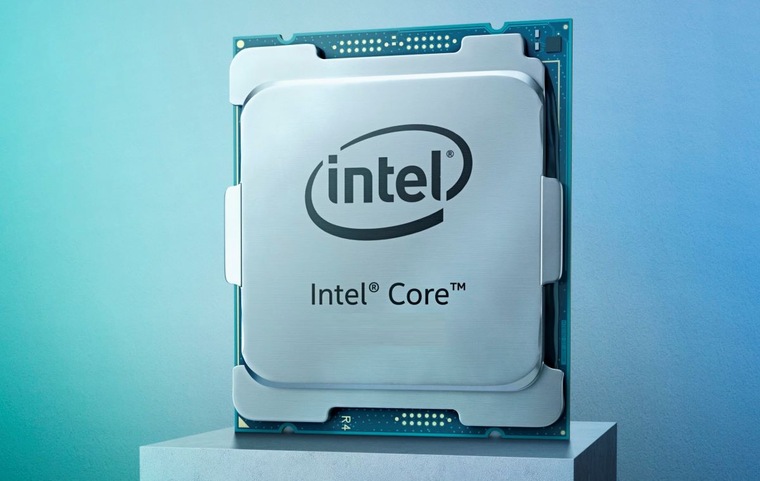
“AMD does have a process advantage, so we should not underestimate that,” Malyala said. “But at the same time, what I’m excited about is both of them are offering good performance. And customers can actually choose a platform not because something is not available, but both are available, so they can actually try it out and see which one that fits best within their budget and fits their application requirements.”
Built-in acceleration and security
For the artificial intelligence space, Intel says Ice lake delivers up to 56 percent more AI inference performance for image classification than the previous generation, and offers up to a 66 percent boost for image recognition. For language processing, Ice Lake delivers up 74 percent higher performance on batch inference gen-over-gen. And on ResNet50-v1.5, the new CPU delivers 4.3 times better performance using int8 via Intel’s DL Boost feature compared with using FP32.
Nash Palaniswamy
“The convergence of AI and HPC is becoming a reality, and customers are thrilled that the 3rd Gen Intel Xeon Scalable processor enables a dynamic reconfigurable datacenter that supports diverse applications,” shared Intel’s Nash Palaniswamy, in an email exchange with HPCwire. “Our latest 3rd Gen Xeon Scalable processor is a powerhouse for AI workloads and delivers up to 25x performance on image recognition using our 40 core CPU compared to our competitor’s 64 core part,” said Palaniswamy, vice president and general manager of AI, HPC, datacenter accelerators solutions and sales at Intel.
The third-generation Xeon Scalable processors also add new security features, including Intel Software Guard Extensions (SGX) and Intel Total Memory Encryption (TME) for built-in security, and Intel Crypto Acceleration for streamlined processing of cryptographic algorithms. Over 200 ISVs and partners have deployed Intel SGX, according to Intel.
The SKU stack
The Ice Lake family includes 56 SKUs, grouped across 10 segments (SKU chart graphic): 13 are optimized for highest per-core scalable performance (8 to 40 cores, 140-270 watts), 10 for scalable performance (8 to 32 cores, 105-205 watts), 15 target four- and eight- socket (18 to 28 cores, 150-250 watts), and there are three single-socket optimized parts (24 to 36 cores, 185-225 watts). There are also SKUs optimized for cloud, networking, media and other workloads. All but four SKUs support Intel Optane Pmem 200 series technology.
Reserved for liquid cooling environments, the 38-core 8368Q Platinum Xeon dials up the frequency of the standard 38-core 8368, increasing the base clock from 2.4 GHz to 2.6 GHz, all-core turbo from 3.2 GHz to to 3.3 GHz, and single-core turbo from 3.4 GHz to 3.7 GHz.
At the top of the SKU mountain is the 8380 with 40 cores, a frequency of 2.3 GHz (base), 3.0 GHz (turbo) and 3.4 GHz (single-core turbo), offering 60 MB cache in a 270 watt TDP. Compared to the Cascade Lake 8280, the 8380 provides 12 additional cores and runs 65 watts hotter. The suggested customer price for the new 8380 is $8099, which is actually about 19 percent less than the list price on the 8280 ($10009).
Intel has not said publicly if it plans to release a multi-chip module (MCM) version of Ice Lake, as a follow-on to the 56-core Cascade Lake-AP part. Intel could conceivably deliver an 80-core ICL-AP but given the 270 watt power envelope of the 8380, that may not be feasible from a thermal standpoint.
Supermicro’s Malyala approves of Intel’s approach to segment-specific SKUs and the near-complete support for Optane PMem across the stack. “It was a pretty big headache for a lot of people with Cascade lake and Cascade Lake Refresh in terms of them trying to figure out how to bring all these features and which ones to enable. It’s a lot cleaner now with Ice Lake,” he said. “There’s a virtualization SKU, a networking SKU, single-socket, long lifecycle. Presenting it this way helps customers to pick and choose because now the product portfolio has exploded, right? So how do people know which one to pick? That is addressed to some extent with the segment-specific SKUs, which also helps us, Supermicro, to validate these in our products.”
In a pre-briefing held last week, Intel said the Ice Lake ramp, which commenced in the final quarter of last year, is going well. The company has shipped more than 200,000 units in the first quarter of 2021 and reports broad industry adoption across all market segments with more than 250 design wins within 50 unique OEM and ODM partners, noting over 20 publicly announced HPC adopters.
Prominent HPC customers who have received shipments so far include LRZ and Max Planck (in Germany), Cineca (in Italy), the Korea Meteorological Administration (KMA), as well as the National Institute of Advanced Industrial Science and Technology (AIST), the University of Tokyo and Osaka University (in Japan).
The third-generation Xeon products are available now through a number of OEMs, ODMs, cloud providers and channel partners. Launch partners Cisco, Dell, Gigabyte, HPE, Lenovo, Supermicro and Tyan (among others) are introducing new or refreshed servers based on the new Intel CPUs, and Oracle has announced compute instances backed by the new Xeons in limited preview with general availability on April 28, 2021. More announcements will be made in the days and weeks to come.
* Benchmarking details at https://edc.intel.com/content/www/us/en/products/performance/benchmarks/intel-xeon-scalable-processors/
Topics:
AI, Applications, Business, Cloud, Processors, Storage, Systems, Vendor News
Sectors:
Academia & Research, Energy, Entertainment, Financial Services, Government, Life Sciences, Manufacturing, Oil & Gas, Retail, Weather & Climate
Tags:
10nm, AMD, benchmarking, Cascade Lake, HPL, Ice Lake, Intel, LINPACK, Milan, monte carlo, NAMD, Oracle, Xeon
Intel Video Shows How it Makes a 10nm Processor
Skip to main content
When you purchase through links on our site, we may earn an affiliate commission. Here’s how it works.
(Image credit: Intel)
Intel has released two videos about its chip design and manufacturing process that give us a rare glimpse into not only the company’s production process, but also into its problematic 10nm process.
Intel’s woes with the 10nm process are well-documented. The company has suffered almost incalculable damage to its long-term roadmaps due to the delay of mass production of its newest node, and even recently cited that it didn’t expect to reach parity with its competitors (most likely in reference to third-party foundry TSMC) until it releases its 7nm process at the end of 2021.
The world of processor design is fraught with technical challenges, and long design cycles are problematic: It can take up to four years from the design stage to final production. As an engineer once quipped, designing a chip is like playing Russian roulette and waiting four years to see if you’ve blown your brains out. But that didn’t stop Intel from plowing forward with audacious goals for its 10nm process.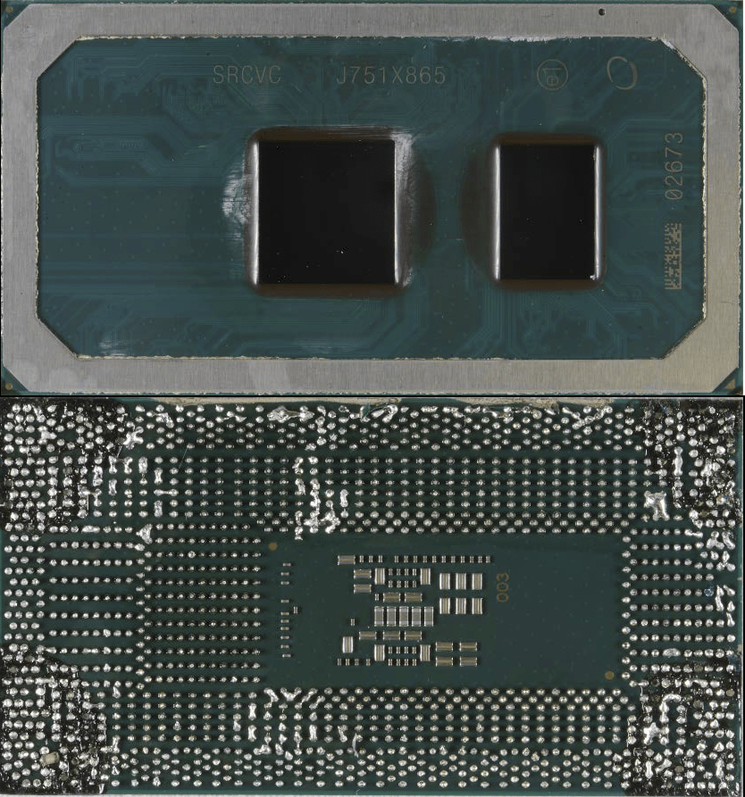 Intel bet big when it began the 10nm design, eschewing the standard doubled gen-on-gen density by aiming for a 2.7X density increase. The company later cited that goal as a key reason it struggled with 10nm, largely because the density goals required several new technologies that contributed to the delays. We can see a few of those potential missteps in the video below.
The video covers the manufacturing process «from sand to silicon,» and while all of it is worth a watch, the deep dive into Intel’s transistor tech begins at roughly 1:50 into the video. Here the company details its FinFET transistor technology and outlines the stunning number of steps required to build up a single transistor (more than a 1000). However, these photolithography, etch, deposition, and other steps are applied to an entire wafer that has multiple die that each wield billions of transistors.
Intel details its contact over active gate (COAG) technology at 3:10 in the video. This tech builds the contact portion of the transistor over the gate instead of extending it from the end of the transistor as Intel has done in the past. That reduces the overall area consumed by the transistors, thereby improving density (more details here at WikiChip). Intel is rumored to have altered, or perhaps even removed (which is unlikely), its COAG feature from its newer iterations of the 10nm process. This part of the design is key, as it helps dictate the performance of transistors that switch on and off at a rate exceeding five billion cycles a second with the 14nm process, but those speeds fall considerably with the 10nm process.
The video also gives us a glimpse of the dizzyingly-complex web of interconnects present on the chip. These tiny wires connect the amazingly-small transistors together, facilitating communication, and are stacked in a complex 3D cluster. However, these small wires can be mere atoms thick, which can lead to failure-inducing electromigration. Smaller transistors require thinner wires, but that also leads to increased resistance that requires more current to drive a signal, which complicates matters. To tackle that challenge, Intel switched from copper wiring to cobalt. Intel used this material to create thinner wires (even though it has higher resistivity) because it doesn’t require as much insulation material wrapped around each wire, but the company only uses it at the lowest levels of the 3D web of interconnects. However, the switch to cobalt is yet another challenge that is rumored to be at the root of Intel’s troubles.
Intel has divulged that it significantly overhauled the 10nm process to address unspecified issues, but we’ll likely never know the full extent of those changes. At the end of the day, however, economical production is the true measure of success, and that is often measured by the yield rate (ie, how many functional chips are harvested per wafer). Intel has struggled in this area, and even by its own projections won’t reach parity on process nodes until 2021. In the meantime, the company is looking to its new technologies that aren’t entirely contingent upon process leadership, like EMIB and Foveros, and it plans to adopt new chiplet-based architectures. We also expect Intel will continue to work on making its architectures portable across nodes to blunt the blow from potential future missteps.
But Intel’s primary challenger, AMD, is also focused on next-gen packaging and fabrics to extend its own chiplet-based architecture, so competition will be brisk. Meanwhile, multiple ARM-based server chips now benefit from TSMC’s node, which threatens further margin erosion and makes Intel’s ability to adhere to an h3 2020 schedule for its Ice Lake chips imperative.
The world of processor design is a minefield of technical challenges, but the intricacies of a chip are truly a modern marvel. We’d love to see more detailed videos of the inner workings of other modern process nodes, in particular the 7nm node from TSMC.
While we wait, Intel also posted another chip manufacturing video that’s decidedly more basic and obviously geared for mainstream audiences. Check it out below.
Get instant access to breaking news, in-depth reviews and helpful tips.
Contact me with news and offers from other Future brandsReceive email from us on behalf of our trusted partners or sponsors
Paul Alcorn is the Deputy Managing Editor for Tom’s Hardware US. He writes news and reviews on CPUs, storage and enterprise hardware.
Topics
CPUs
Tom’s Hardware is part of Future US Inc, an international media group and leading digital publisher. Visit our corporate site .
©
Future US, Inc. Full 7th Floor, 130 West 42nd Street,
New York,
NY 10036.
Intel changes names: no longer 10 nm process technology, but Intel 7
The modern computer user has become much more educated, taking into account not only the number of cores and gigahertz, but also the process technology by which the processor is made. The smaller it is, the faster and colder the processor, if you recalculate the performance per watt ratio. New generations of processors and new models are becoming more productive and consume less and less energy, besides, they emit less heat, progress cannot be stopped. And yet not everyone can answer why this is happening. Why the smaller the process technology, the more energy efficient the processor, let’s figure it out.
Historical reference
Of course, a modern processor cannot be called a «microcircuit». A clearer classification of devices is now generally accepted: microcircuits, microcontrollers, processors. Calling “microcircuits” this way, we mean the degree of their complexity, but in fact they are all miniature circuits on a chip, from where this name came from.
The first miniature circuit appeared back in 1958, it was made in Germany and contained only a few radio components. But this was a kind of breakthrough in radio electronics, later silicon will be chosen as a substrate, even later a whole revolution of integrated circuits will take place, by the way, hard logic microcircuits are still being produced, and they are in demand.
November 15, 1971 Intel officially announces the world’s first single-chip four-bit microprocessor, Intel 4004, which contained 2300 transistors and was made using 10 micrometer technology. It really looked more like a modern microcircuit with 16 pins. By the way, 1000 nanometers is equal to 1 micrometer.
Then you can skip the whole race of different companies, even «universal» motherboards for «universal» processors from different manufacturers, which were «programmed» with jumpers for the processor manufacturer, AMD or Intel, there was such a thing.
On November 20, 2000, the revolutionary Pentium 4 processor was announced, which was made using the latest NetBurst technology, had 423 contacts and a 180 nm manufacturing process. Due to the too high density of radio components on a chip, the Pentium 4 had a fairly high heat dissipation, but the technology was improved by leaps and bounds up to the 65 nm process technology. After reaching this value, nanometers began to decrease much more slowly over the years.
What do these nanometers mean
Everyone saw a board with radio components. The very first boards and parts were very large, the board itself was a connecting track with places for installing elements on legs.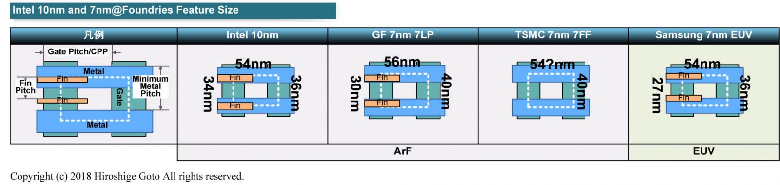 Further development is the appearance of SMD parts, which were already soldered directly to the tracks, without transitions from the reverse side, and the finished devices became much more compact. Modern boards are more like a substrate with sugar sprinkled on it — everything has become so miniature. The crystals of microcircuits, and in our case, processors, evolved in approximately the same way.
Until recently, the processor chip represented the same board, all elements were placed on a flat surface, and the distance between the «tracks» was precisely those nanometers and the technical process. The smaller the distance between the tracks, the smaller were the radio components, especially transistors. The transistor itself resembles an ordinary tap: there is an input, an output and a control lever, understanding 1 and 0: “open” or “closed”. And the smaller the distance between the inlet and outlet of such a «crane», the less «pressure» it can withstand.
Upon reaching the process technology below 22 nm, engineers were faced with a problem: even if the transistor was closed, current still flowed through it. It was not possible to use more planar placement of elements, so they came up with the idea of building a vertical wall between the conductors: the distance between the conductors can be reduced, they lie in the same plane, but there is a sufficient vertical distance between them and between the ascent and descent it could just compensate for the insufficient length of the transition.
After such a decision, a new concept appeared, like “shutter length”. For Intel, this value is 24 nm, and for example, for Samsung, it is 30 nm. Although the original indicator by which the process technology was measured, namely the distance between the conductors, remained unchanged.
Intel vs AMD
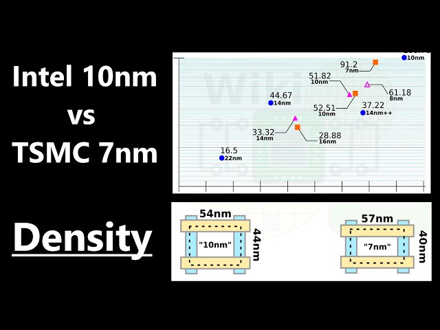
The eternal struggle of two corporations for customers has now acquired a new intensity of passions. AMD’s latest processors, which claim to be 7nm technology, end up losing in terms of performance/Watt to Intel 7 technology, which is supposedly 10nm. Well, maybe AMD’s transistor resembles a Greek “omega” in order to keep the gate length at least 22 nm, but the density of radio components on a chip and their efficiency are still up to Intel: it places 106 billion parts on the same area, while while AMD is only 96 billion.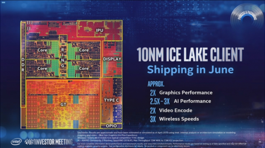 In addition, Intel transparently makes it clear that Intel 7 and 10 nm are not the same thing: with the previous simple “ten”, the efficiency of the technology in terms of performance/Watt has become 10-15% more efficient.
What’s next
And then Intel has a plan to introduce new technology and a new designation for the process technology until 2024. After Intel 7, Intel 4 is next: a kind of 4-nanometer process technology, which, compared to Intel 7, will give another 20% increase. In the second half of 2023, it is planned to release processors based on Intel 3 technology to the masses, which at that time, with the already past intel 4, will give another 18% increase in efficiency. The key point is the appearance in 2024 of Intel 20A technology, and this is not quite equivalent to Intel 2, by analogy with past technical processes. By that time, it is planned to completely rework the structure of transistors and internal connections.
Total
At the moment, it is difficult to abandon the familiar old and accept the incomprehensible new.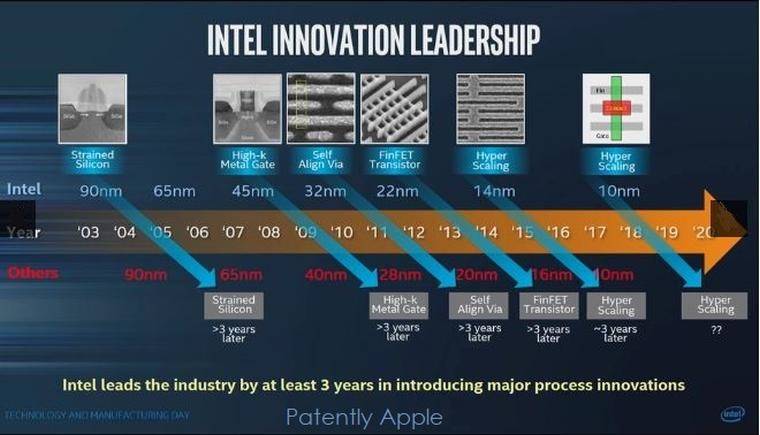 But the conclusion suggests itself: while everyone thought that Intel lost to AMD, and still releases processors using the old 10 nm technology, simply changing the name to Intel 7, while AMD has already mastered the 7 nm process technology, in fact, Intel wiped its competitor’s nose with the plan to introduce the new Intel X technology, and in 2 years it is ready to release processors based on a similar AMD technology in 2 nm.
Many AMD fans and Intel haters are already waiting for a decent response from the «reds», but they are still silent … maybe something will appear in the new year, but Intel has already planned the introduction of new technology for a couple of years ahead and defiantly posted it in the public domain, and does not expect any competition at all. But it’s not time to open the champagne…
The era of 10nm chips — who develops such processors and what the future holds for the industry / Habr
Semiconductor manufacturers have successfully mastered the 10nm process technology. In the article we tell who produces microcircuits based on it and when to wait for 5- and 3-nm technologies.
Photo — Santi — CC BY-SA
Who introduced 10nm
For several years, Intel has been postponing full-scale production of chips on the 10nm process. Among the reasons, experts cited difficulties with multi-patterning technology, which increases the density of transistors, and the low yield of high-quality processors. But in October of this year, the company announced that it was able to establish a stable production of chips on a new technical process.
So far, only CPUs for personal computers based on the Ice Lake architecture have been produced. But the company promises to deliver Xeon (Ice Lake-SP) for data centers in the second half of 2020.
Similar devices are produced by AMD in partnership with Taiwanese TSMC. At the end of last year, they introduced a chip made using an improved 7nm process technology. In terms of physical parameters (due to different evaluation methods), it resembles 10nm from Intel.
Based on the new process technology, a line of AMD server processors — EPYC is built. Sales of AMD EPYC 7002 devices based on Zen 2 architecture started at the end of summer. Companies such as Google and Twitter placed the chips in their data centers. Devices should reduce server power consumption and cut TCO by a quarter. Also, the supercomputer developer Cray is already working with the new CPUs. The devices were introduced into the computing system for the F1 team — Haas.
Heading for further miniaturization
In 2021, Intel plans to move to a 7nm process technology based on EUV. This is photolithography in the «hard» ultraviolet. Interestingly, the first product built on the new process technology will not be a processor, but a graphics card for data centers, supercomputers and other HPC systems.
Intel is also working on 5nm technology, but the completion date of the project is unknown.
TSMC is working on 5nm — the company began preparations in June last year, investing $ 25 billion in development. Part of the funds was directed to the construction of a factory in Taiwan. Chip production will start in the second quarter of 2020.
At the beginning of this year, Samsung announced its readiness to produce mobile processors using 5nm technology. The company has already equipped the production line, is building a special plant and is even accepting orders for test batches of chips. However, a full release date has yet to be announced.
Beyond 5nm
TSMC is preparing to launch a 5nm process and is developing 3nm and even 2nm technologies. The company has evaluated all possible types of transistor structures and is building a factory (also in Taiwan). The company will start production at the end of 2022 or the beginning of 2023.
Photo — Enrique Jiménez — CC BY-SA
Samsung also plans to start manufacturing 3nm chips — it should be launched in 2021.![]() The organization’s specialists use GAAFET technology (Gate-All-Around Field-Effect Transistors), which reduces voltage losses, increasing the energy efficiency of the transistor.
The organization’s specialists use GAAFET technology (Gate-All-Around Field-Effect Transistors), which reduces voltage losses, increasing the energy efficiency of the transistor.
Research institutes are also participating in the race for miniaturization. For example, last year specialists from the Imec center, in partnership with Cadence Design Systems, have already developed test samples of microprocessors using 3-nm technology.
Industry leaders note that the cost of mastering new technologies will be large, and only large companies will be able to switch to new technical processes, which will beat them off thanks to a wide range of products. In turn, to overcome technological difficulties in the process of direct production, the industry will need alternative solutions. Therefore, in the future, we can expect the emergence of radically new processor technologies.
On our website, we describe how the 1cloud.