Socket S1g4 — AMD — WikiChip
Socket S1g4 was the fourth and last socket for OPGA-638-packaged AMD mobile microprocessors with an integrated DDR2 and DDR3 memory controller, and the successor to Socket S1g3. Its counterparts for desktop processors are Socket AM3 and Socket AM3+, for servers Socket C32 and Socket G34. For the small form factor desktop, mobile and embedded market AMD developed package ASB2. Socket S1g4 was superseded by Socket FS1 supporting mobile processors with integrated graphics.
The main improvement of Socket S1g4 over S1g3 is support for DDR3 memory. As the number of CPU cores in the package grew to three and four, voltage regulators were integrated on the chip and support for two core power planes was dropped.
Socket S1g4 was used in AMD’s «Danube» mobile platform. All processors for Socket S1g4, codename «Champlain», are members of AMD’s Family 10h with CPU cores based on the K10 microarchitecture and were fabricated on a 45 nm SOI process.
All revisions of Socket S1 have the same dimensions, however processors for Socket S1g4 appear to be electrically incompatible with Socket S1g1 and vice versa. Processors for Socket S1g2 have a DDR2 memory controller and will not work in Socket S1g4. To which extent Socket S1g4 processors are compatible with Socket S1g2 and S1g3, in DDR2 mode and with a suitable BIOS, is unclear.
Contents
- 1 Features
- 2 Chipsets
- 3 Processors using Socket S1g4
- 4 Package Diagram
- 5 Socket Outline
- 6 Pin Map
- 6.1 Differences between Socket S1 revisions
- 7 References
- 8 See also
Features[edit]
- 638-pin lidless micro pin grid array package, 1.27 mm pitch, 26 × 26 pins, 35 × 35 mm, organic substrate, C4 (flip chip) die attachment
- 16 bit HyperTransport 3.0 interface up to 1800 MHz, 3600 MT/s, 7.2 GB/s in each direction
- 2 × 64 bit DDR2 SDRAM interface up to 400 MHz, PC2-6400 (DDR2-800), 12.
 8 GB/s or
 - 2 × 64 bit DDR3 SDRAM interface up to 667 MHz, PC3-10600 (DDR3-1333), 21.3 GB/s
- Up to 2 SODIMMs, no ECC support
- DDR2 JEDEC SSTL_1.8, DDR3 JEDEC 1.5V, 1.35V
- Power Management
- AMD PowerNow! technology
- ACPI C1, C1E, C2, C3, C5/Altvid, S1, S3, S4, S5
- Separate core and northbridge power planes
- Two northbrige P-states
- Thermal Controls
- Thermal protection
- Hardware thermal control
- Thermal diode
Chipsets[edit]
- AMD 880M
- AMD SB820 southbridge
Processors using Socket S1g4[edit]
- AMD Phenom II Quad-Core Mobile
- AMD Phenom II Triple-Core Mobile
- AMD Phenom II Dual-Core Mobile
- AMD Turion II Dual-Core Mobile
- AMD Athlon II Dual-Core Mobile
- AMD V-Series
Package Diagram[edit]
No data available. Dimensions should be similar to those of the OPGA-638 package shown on the Socket S1g1 page.
Socket Outline[edit]
Socket S1 limits as specified in AMD Publ. #31839. Depicted is Foxconn Interconnect Technology Part No. PZ6382A-284S-01F. All dimensions in millimeters.
Pin Map[edit]
Differences between Socket S1 revisions[edit]
| Pin | S1g1 | S1g2/S1g3 | S1g4 | Description |
|---|---|---|---|---|
| R21 | MA_ADD[0] | MA_ADD[10] | MA_ADD[10] | DRAM Column/Row Address |
| N21 | MA_ADD[1] | MA_ADD[0] | MA_ADD[0] | |
| M22 | MA_ADD[3] | MA_ADD[4] | MA_ADD[4] | |
| M24 | MA_ADD[4] | MA_ADD[6] | MA_ADD[6] | |
| M20 | MA_ADD[5] | MA_ADD[1] | MA_ADD[1] | |
| M19 | MA_ADD[6] | MA_ADD[3] | MA_ADD[3] | |
| L22 | MA_ADD[8] | MA_ADD[11] | MA_ADD[11] | |
| L19 | MA_ADD[9] | MA_ADD[8] | MA_ADD[8] | |
| R19 | MA_ADD[10] | MA_RAS_L | MA_RAS_L | |
| L20 | MA_ADD[11] | MA_ADD[5] | MA_ADD[5] | |
| K24 | MA_ADD[12] | MA_ADD[14] | MA_ADD[14] | |
| K20 | MA_ADD[14] | MA_ADD[12] | MA_ADD[12] | |
| T22 | MA_BANK[0] | MA_CAS_L | MA_CAS_L | DRAM Bank Address / Column Address Strobe |
| R20 | MA_BANK[1] | MA_BANK[0] | MA_BANK[0] | |
| R23 | RSVD | MA_BANK[1] | MA_BANK[1] | |
| K22 | MA_BANK[2] | MA_ADD[9] | MA_ADD[9] | |
| U20 | MA_CAS_L | MA1_CS_L[0] | MA1_CS_L[0] | DRAM Column Address Strobe / Chip Select |
| J21 | MA_CKE[0] | MA_BANK[2] | MA_BANK[2] | DRAM Clock Enable / Bank Address |
| T20 | MA_RAS_L | MA0_CS_L[0] | MA0_CS_L[0] | DRAM Row Address Strobe / Chip Select |
| U21 | MA_WE_L | MA1_ODT[0] | MA1_ODT[0] | DRAM Write Enable / Enable Pin for On Die Termination |
| E16 | MA0_CLK_H[1] | MA_CLK_H[1] | MA_CLK_H[1] | DRAM Differential Clock |
| F16 | MA0_CLK_L[1] | MA_CLK_L[1] | MA_CLK_L[1] | |
| P19 | RSVD | MA_CLK_H[4] | MA_CLK_H[4] | |
| P20 | RSVD | MA_CLK_L[4] | MA_CLK_L[4] | |
| N19 | RSVD | MA_CLK_H[5] | MA_CLK_H[5] | |
| N20 | RSVD | MA_CLK_L[5] | MA_CLK_L[5] | |
| Y16 | MA0_CLK_H[2] | MA_CLK_H[7] | MA_CLK_H[7] | |
| AA16 | MA0_CLK_L[2] | MA_CLK_L[7] | MA_CLK_L[7] | |
| T19 | MA0_CS_L[0] | MA0_ODT[0] | MA0_ODT[0] | |
| V22 | MA0_CS_L[1] | MA0_ODT[1] | MA0_ODT[1] | |
| J22 | MA0_CS_L[2] | MA_CKE[0] | MA_CKE[0] | |
| V19 | MA0_CS_L[3] | MA1_ODT[1] | MA1_ODT[1] | |
| U19 | MA0_ODT[0] | MA0_CS_L[1] | MA0_CS_L[1] | |
| V20 | MA0_ODT[1] | MA1_CS_L[1] | MA1_CS_L[1] | |
| h26 | RSVD | RSVD_M1 | MA_RESET_L | DRAM Reset Pin for Suspend-to-RAM Power Management Mode |
| T24 | MB_ADD[0] | MA_WE_L | MA_WE_L | |
| P26 | MB_ADD[1] | MB_ADD[2] | MB_ADD[2] | |
| P24 | MB_ADD[2] | MB_ADD[0] | MB_ADD[0] | |
| N26 | MB_ADD[3] | MB_ADD[4] | MB_ADD[4] | |
| N25 | MB_ADD[4] | MB_ADD[6] | MB_ADD[6] | |
| N24 | MB_ADD[5] | MB_ADD[1] | MB_ADD[1] | |
| N23 | MB_ADD[6] | MB_ADD[3] | MB_ADD[3] | |
| L26 | MB_ADD[7] | MB_ADD[11] | MB_ADD[11] | |
| L24 | MB_ADD[9] | MB_ADD[7] | MB_ADD[7] | |
| U25 | MB_ADD[10] | MB_RAS_L | MB_RAS_L | |
| L25 | MB_ADD[11] | MB_ADD[12] | MB_ADD[12] | |
| L23 | MB_ADD[12] | MB_ADD[5] | MB_ADD[5] | |
| W25 | MB_ADD[13] | MB0_CS_L[1] | MB0_CS_L[1] | |
| J26 | MB_ADD[14] | MB_BANK[2] | MB_BANK[2] | |
| J25 | MB_ADD[15] | MB_CKE[0] | MB_CKE[0] | |
| R24 | RSVD | MB_BANK[0] | MB_BANK[0] | |
| U26 | MB_BANK[0] | MB_BANK[1] | MB_BANK[1] | |
| T26 | MB_BANK[1] | MB_ADD[10] | MB_ADD[10] | |
| K26 | MB_BANK[2] | MB_ADD[9] | MB_ADD[9] | |
| V26 | MB_CAS_L | MB0_CS_L[0] | MB0_CS_L[0] | |
| J23 | MB_CKE[0] | MB_ADD[14] | MB_ADD[14] | |
| U24 | MB_RAS_L | MB_CAS_L | MB_CAS_L | |
| U22 | MB_WE_L | MB1_CS_L[0] | MB1_CS_L[0] | |
| A17 | MB0_CLK_H[1] | MB_CLK_H[1] | MB_CLK_H[1] | |
| A18 | MB0_CLK_L[1] | MB_CLK_L[1] | MB_CLK_L[1] | |
| R26 | RSVD | MB_CLK_H[4] | MB_CLK_H[4] | |
| R25 | RSVD | MB_CLK_L[4] | MB_CLK_L[4] | |
| P22 | RSVD | MB_CLK_H[5] | MB_CLK_H[5] | |
| R22 | RSVD | MB_CLK_L[5] | MB_CLK_L[5] | |
| AF18 | MB0_CLK_H[2] | MB_CLK_H[7] | MB_CLK_H[7] | |
| AF17 | MB0_CLK_L[2] | MB_CLK_L[7] | MB_CLK_L[7] | |
| U23 | MB0_CS_L[0] | MB_WE_L | MB_WE_L | |
| W24 | MB0_CS_L[1] | MB_ADD[13] | MB_ADD[13] | |
| J24 | MB0_CS_L[2] | MB_ADD[15] | MB_ADD[15] | |
| Y26 | MB0_CS_L[3] | MB1_ODT[0] | MB1_ODT[0] | |
| B18 | RSVD | RSVD_M2 | MB_RESET_L | |
| AA8 | RSVD | MEMHOT_L | MEMHOT_L | DRAM Thermal Protection input |
| A3 | PSI_L | RSVD | RSVD | Power Status Indicator (low power mode) for VDD regulator |
| W8 | TEST4 | THERMDA | THERMDA | Thermal Diode, Anode |
| W7 | TEST5 | THERMDC | THERMDC | Thermal Diode, Cathode |
| AA7 | TEST13 | RSVD | RSVD | |
| AE6 | TEST26 | ALERT_L | ALERT_L | Programmable pin that can indicate different events, including a SB-TSI interrupt |
| M11 | VSS | KEY1 | VSS | |
| W18 | RSVD | KEY2 | RSVD | |
misc. |
VDD | VDD0 | VDD | Core power supply |
| F6 | VDD_FB_H | VDD0_FB_H | VDD0_FB_H | Differential feedback to VDD0 regulator |
| E6 | VDD_FB_L | VDD0_FB_L | VDD0_FB_L | |
| misc. | VDD | VDD1 | VDD | |
| Y6 | TEST3 | VDD1_FB_H | VDD1_FB_H | Differential feedback to VDD1 regulator |
| AB6 | TEST2 | VDD1_FB_L | VDD1_FB_L | |
| misc. | VDD | VDDNB | VDDNB | Northbridge power supply |
| H6 | RSVD | VDDNB_FB_H | VDDNB_FB_H | Differential feedback to VDDNB regulator |
| G6 | RSVD | VDDNB_FB_L | VDDNB_FB_L | |
| B5 | VID[0] | RSVD | RSVD | Voltage ID for VDD regulator |
| C5 | VID[1] | RSVD | RSVD | |
| A4 | VID[2] | SVD | SVD | Serial Voltage ID Interface, Data |
| A6 | VID[3] | SVC | SVC | Serial Voltage ID Interface, Clock |
| C6 | VID[4] | LDTREQ_L | LDTREQ_L | HT link is active or requested by a device (HT Gen 3. 0) 0)
|
| A5 | VID[5] | RSVD | RSVD | |
| misc. | VTT | VTT | VDDR | |
| Y10 | VTT_SENSE | VTT_SENSE | VDDR_SENSE | VTT / VDDR monitor pin |
References[edit]
- «Low-Profile Socket S1 Design Specification», AMD Publ. #31839, Rev. 3.01, April 10, 2007
- «BIOS and Kernel Developer’s Guide (BKDG) For AMD Family 10h Processors», AMD Publ. #31116, Rev. 3.62, January 14, 2013
- «Revision Guide for AMD Family 10h Processors», AMD Publ. #41322, Rev. 3.92, March 2012
- «AMD RS880M Databook Device Specification for the RS880M and RS880MC», AMD Publ. #46113, Rev. 1.30, 2010
See also[edit]
- Socket S1g1
- Socket S1g2
- Socket S1g3
- Socket AM3
- Socket FS1
- Package ASB2
What Is Socket S1? (with picture)
`;
Internet
Fact Checked
Alex Newth
The socket S1 is an AMD®-built socket made to house central processing units (CPUs) for the mobile computing, or laptop, market. There are 638 contacts included on the socket S1, and it comes with a rotating locking unit instead of a lever device like most other sockets. As of July 2011, there are four CPUs made to work with this socket, though there are others that can fit into the S1 socket. In terms of power, the socket S1 can reach about 1.8 to 3.2 gigahertz (GHz), with most processors clocking in around 2.1 to 2.5 GHz; this socket also can support four cores at once. There were four total revisions of this socket before it was retired, with the last one adding new core and memory support.
When it comes to the main design of the socket S1, the contacts, this socket looks like many others. There are a total of 660 contacts, but 22 of them are plugged, so 638 are electronically active; in the center there is a small square without any contacts. The actuator, or locking unit, is different from other sockets. With most sockets, there is a lever that is pulled up to unlock the CPU; with the S1 socket, the actuator is half-turned to unlock the CPU.
There have been four processors officially created for the socket S1. These are the Athlon 64 X2®, Turion 64 MK®, Turion 64 X2® and Mobile Sempron®. All four of these processors are used in laptops rather than in desktop computers.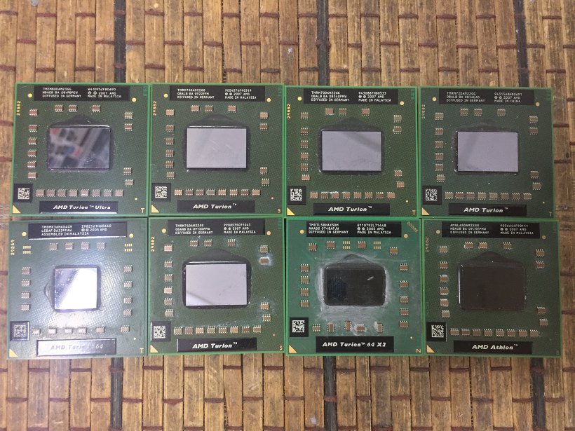
All sockets are made to support a certain range of power, which helps the CPU perform its duties. The socket S1 can reach up to 3.2 GHz and has a low range of 1.8 GHz. CPUs commonly hit the middle of this range, between 2.1 and 2.5 GHz. The data-transferring rates for memory range from around 800 to 1,333 megahertz (MHz).
In total, there have been four revisions of the socket S1, with the last one referred to as S1g4. This revision made improvements over the other ones by including extra core support, up to four separate cores for higher processing abilities. This socket also supports double data rate type three (DDR3) synchronous dynamic random access memory (SDRAM), which the earlier versions did not support. While the last revision has many new supports, it is physically identical to the other versions; all the differences are electronically present.
You might also Like
Recommended
AS FEATURED ON:
Page not found — Technical City
Page not found — Technical City
We did not find such a page on our website: /ru/cpu/amd-rating%3fpg%3d4
Popular video card comparisons
GeForce RTX
3060 Ti
vs
GeForce RTX
nine0012 3060
GeForce RTX
3060 Ti
vs
GeForce RTX
3070
GeForce GTX
1050 Ti
vs
GeForce GTX
1650
GeForce GTX
1660 Ti
vs
GeForce GTX
1660 Super
GeForce RTX
2060 Super
vs
GeForce RTX
3060
nine0010
GeForce GTX
1060 6GB
vs
Radeon RX
580
Popular video cards
GeForce RTX
4090
GeForce GTX
1050 Ti
nine0010
GeForce RTX
3060
GeForce GTX
1660 Super
Radeon RX
580
GeForce RTX
3060 Ti
Popular
processor comparisons
nine0010
Ryzen 5
5600X
vs
Core i5
12400F
Ryzen 5
3600
vs
Core i5
10400F
Core i5
10400F
vs
Core i3
12100F
Ryzen 5
3600
vs
Ryzen 5
5600X
Ryzen 5
5600X
vs
nine0010
Ryzen 5
5600G
Ryzen 5
5600X
vs
Ryzen 5
5600
Popular processors
Ryzen 5
5500U
EPYC
nine0012 7h22
Core i3
1115G4
Core i5
1135G7
Ryzen 5
5600X
Ryzen 5
3500U
nine0000 processor characteristics and tests in 4 benchmarks
AMD started selling the Phenom II X4 P920 on May 12, 2010.