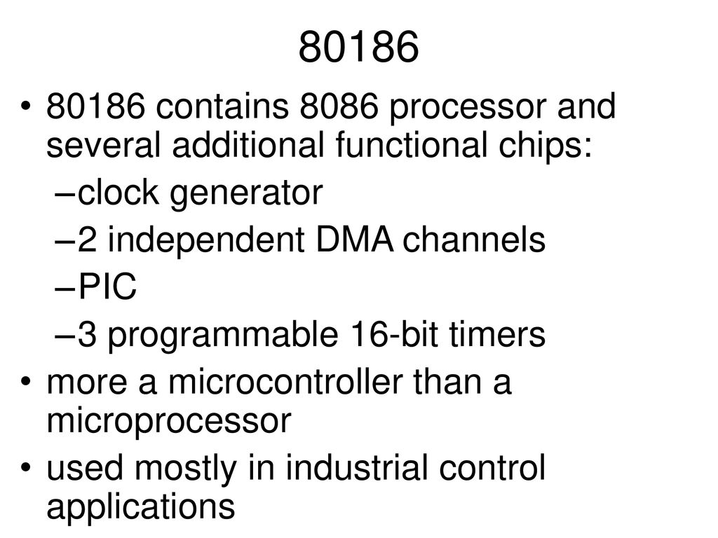
80186 Microprocessors: Introduction and Architecture
Hello friends, today we are going to discuss the 80186 microprocessor with integrated peripherals.
The Intel 80186 is an improved version of the 8086 microprocessor. 80186 is a 16-bit microprocessor with a 16-bit data bus and a 20-bit address bus. It has a programmable peripheral device integrated into the same package. The instruction set of the 80186 is a superset of the instruction set of the 8086. The term super-set means that all of the 8086 instructions will execute properly on an 80186, but the 80186 has a few additional instructions. The following figure shows the block diagram and pin diagram of 80186. The CPU is divided into seven independent functional parts.
80186 internal block diagram
80186 68-pins pin diagram
Functional parts of 80186 Microprocessor
- The Bus Interface Unit (BIU)
- Execution Unit (EU)
- Clock Generator
- Programmable interrupt controller
- Programmable Chip Select Unit (CSU)
- Programmable DMA Unit
- Programmable counter/timers
The Bus Interface Unit (BIU)
The 80186 has the same bus interface unit (BIU) and execution unit (EU) as the 8086. We can see this under the heading The 8086 Microprocessor- Internal Architecture. The 80186 is 68 pins lead-less package, so it has enough pins to send out both the minimum mode type signals RD and WR and the S0 – S3 status signals which can be connected to external bus controller ICs for maximum mode systems. It does not have a pin labeled MN/MX for switching the minimum mode through the maximum mode.
Clock Generator
The 80186 has a built-in clock generator so that we can add external crystal. This reduces the component count in a system. It has three-pin connections: X1, X2, and CLK OUT. The X1 and X2 pins are connected to a crystal that resonates twice the operating frequency of the microprocessor. The CLK OUT pin provides a system clock signal that is one-half the crystal frequency. In addition to external pins, the clock generator provides the internal timing for synchronizing the READY input pin.
Programmable Interrupt Controller
The programmable interrupt controller has four interrupt inputs: INT0, INT1, INT2/INTA0, and INT3/INTA1 as well as one nonmaskable interrupt NMI input. These inputs operate with two modes: internal mode and external mode. In internal mode, if the four INT inputs are programmed, then a signal is applied to one of them to push the return address on the stack and vector directly to the start of the interrupt service procedure for that interrupt. In external mode, the INT2/INTA1 pins can be programmed to be used as interrupt inputs or they can be programmed to function as an interrupt acknowledge outputs. This mode is used to interface with external 8259As. When the 8259A is externally attached to 80186, the 80186 microprocessors work as the master, and the 8259A works as the slave.
Programmable Chip Select Unit
This built-in address decoder unit can be programmed to produce an active low chip select signal when the memory or port address in a specified range is sent out. This built-in decoder is to select major blocks of memory. six memory address chip select signals are available: lower chip select lines LCS upper chip select lines UCS and middle chip select lines MCS 0-3 The boundary of the lower chip select signal begin at location 00000H and the boundary of the upper chip select signal is ends at location FFFFFH. The sizes of the memory areas are programmable by some bits put in a control word, and wait states (0-3 waits) can be automatically inserted with the selection of an area of memory.
In addition to producing memory chip select signals, the 80186 can be programmed to produce up to seven peripheral chip select signals on its PCS0 -PCS4, PCS5/A1, and PCS6 /A2 pins. The programmable I/O area starts at a base I/O address programmed by the user, and all seven 128-byte blocks are contiguous.
Programmable DMA Unit
The DMA unit has two DMA request inputs, DRQ0 and DRQ1. These inputs allow external devices such as disk controllers, CRT controllers, etc. to request the use of one of the DMA channels. For each DMA channel, the 80186 has a full 20-bit register to hold the source address, a 20-bit register to hold the destination address, and a 16-bit counter to keep track of how many words or bytes have been transferred. DMA transfers can be from memory to memory, I/O to I/O, or between I/O and memory.
Programmable counter/timers
The timer section contains three fully programmable 16-bit timers. Timers 0 and 1 generate waveforms for external use and are driven by either the master clock of 80186 or by an external clock. They are also used to count external events. The third timer, timer 2, is internally connected to the processor clock. The output of timer 2 generates an interrupt after a specified number of clocks and can provide a clock to the other timers.
How you found this article, is it useful? please feel free to write me a comment so I can improve for the betterment. If you would like more information please visit our other posts or let me know through comments in the right below.
Subscribed to the My Computer Tutors for updates. I will keep updating to you with latest tutorials.
80186 Microprocessor Architecture — EEEGUIDE.COM
The Intel 80186 Microprocessor is a high-performance, highly integrated 16-bit microprocessors. Usually, the 80186 Microprocessor is intended for embedded systems, as microcontrollers with external memory. To reduce the number of chips in systems, it is required to include clock generator, interrupt controller, timers, wait state generator, DMA channels, and external chip select lines within a chip. The 80186 is a natural successor to the 8086 in personal computers. However, because of its integrated hardware was incompatible with the hardware used in the original IBM PC. The architecture of 80186 Microprocessor is shown in Fig. 11.1.
Th architecture of 80186 is common with the 8086 and 8088 microprocessors. This 80186 Microprocessor is a very high-integration 16-bit microprocessor. This IC combines 15 to 20 most common microprocessor components onto a single chip and provides twice the performance of standard 8086. The object code of 80186 is compatible with 8086 and 8088 microprocessors but it adds 10 new instructions. The following functional description describes the basic architecture of 80186 Microprocessor:
- Clock generator
- Bus interface unit
- DMA controller
- 16-bit programmable timer consisting of three timers
- Programmable interrupt controller
- Chip select unit into a single chip
The 8086, 8088, 80186, and 80286 families all contain the same basic set of registers, instructions, and addressing modes. The 80186 Microprocessor is also compatible with the 8086, 8088, and 80286 CPUs.
Register Set:
The 80186 base architecture has fourteen registers as shown in Fig. 11.2. These registers are grouped into the five categories such as segment registers. base and index registers, status and control registers and status word.
General Registers The 80186 Microprocessor consists of eight 6-bit general-purpose registers which are used to perform all arithmetic and logical operations. Four of these registers AX, BX, CX, and DX can be used as 16-bit registers or split into pairs of separate 8-hit registers.
Segment Registers Four 16-bit special-purpose registers (CS, DS, SS and ES) are used to select the segments of memory at any given time. The memory can be immediately addressable as code, stack, and data.
Base and Index Registers Four of the general-purpose registers BX, BR SI and DI can be used to determine offset addresses of operands in memory. These registers may contain base addresses or indexes to particular locations within a segment. The different addressing modes of the 80186 Microprocessor selects the specific registers to determine the physical address of memory for an operand.
Status and Control Registers Two 16-bit special-purposes registers (IP and Status word) are also used to record or alter different aspects of the 80186 Microprocessor state. The IP (Instruction Pointer) register contains the offset address of the next sequential instruction to be executed, but the status word register contains status and control flag bits as depicted in Fig. 11.2 and Fig. 11.3 respectively.
Status Word:
The status word is used to record specific characteristics of the result of logical and arithmetic instructions and controls the operation of the 80186 within a specified operating mode. The status word register is 16 bits wide. Bits 0, 2, 4, 6, 7, and 11 are used for logical and arithmetic operations and bits 8, 9, and 10 are used to control the processor operation. The function of the status word bits is given below.
CF (Carry Flag) The carry flag is set whenever a carry/barrow is generated after arithmetic operations such as addition and subtraction; cleared otherwise.
PF (Parity Flag) This flag is set if low-order 8 bits or the final result after arithmetic/logical operations contain an even number of 1 bit. If there is odd number of ones, it is reset.
AF (Auxiliary Flag) This AF is set whenever there occurs a carry or borrow at the low-order four bits of AL during any operations; cleared otherwise.
ZF (Zero Flag) This flag is set if the result is zero after any operation; otherwise it is reset.
SF (Sign Flag) The sign flag is equal to high-order bit of result. It is set if the result is negative or MSB = 1. It is reset if the result is positive or MSB = 0.
TF (Single-Step Flag) It is used in the processor in single-step mode. When this flag is set, a single-step interrupt occurs after the next instruction executes. TF is cleared by the single-step interrupt.
IF (Interrupt-Enable Flag) When this flag is set, maskable interrupts is enabled cause the CPU to control to an interrupt vector specified location.
DF (Direction Flag) If DF is set, it causes string instructions to auto-decrement the appropriate index register. Clearing DF causes auto-increment. When DF = 1, index register automatically decrement. If DF = 0, index register automatically increment.
OF (Overflow Flag) When the signed result is too large and cannot be expressed within the number of bits in the destination operand, overflow flag is set; cleared otherwise.
Clock Generator:
The 80186 has an on-chip clock generator for both internal and external clock generation. The features of the clock generator are a crystal oscillator, a divide-by-two counter, synchronous and asynchronous ready inputs, and reset circuitry.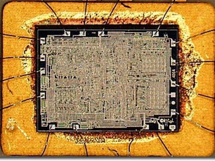
Oscillator Figure 11.4 shows the 80186 crystal oscillator configurations. The oscillator circuit of the 80186 is designed to be used with a parallel resonant fundamental mode crystal. This can be used as the time base for the 80186. The crystal frequency selected will be double the CPU clock frequency. When an external oscillator is used, it can be connected directly to the input pin X1 in lieu of a crystal. The output of the oscillator is not directly available outside the 80186 Microprocessor.
Clock Generator The 80186 clock generator provides the 50% duty cycle processor clock for the 80186. It is possible by dividing the oscillator output by 2 forming the symmetrical clock. When an external oscillator is used, the state of the clock generator will change on the falling edge of the oscillator signal. If an external crystal of 12 or 16 MHz is connected with 80186, then it generates a 6 or 8 MHz internal clock. Hence 80186/80188 is able to operate either at 6 or 8 MHz internal clock. The requirement of crystal frequencies for 80186/80188 is 16 MHz and for advanced version, the 80186/80188 is 12 MHz. The CLKOUT pin gives the processor clock signal for use outside the 80186. This can be used to drive other system components. Always all timings should be referenced to the output clock.
DMA Channels:
The 80186 DMA controllers have two independent high speed DMA channels. Data transfers can take place between memory and I/O devices (memory to I/O or I/O to memory) or within the same space (memory to memory or I/O to I/O). Data can be transferred either in 8 bits (bytes) or in 16 bits (words) from even or odd addresses. Each DMA channel consists of a 20-bit source and destination pointer. The content of the index pointer can be incremented or decremented depending upon data-transfer byte or word. When data transfer is one byte, the pointer is incremented by one. If data transfer is one word, the pointer is incremented by two. Each data transfer always takes 2 bus cycles, i. e., minimum 8 T states. The first bus cycle is used to fetch data and the other bus cycle can be used to store data. The maximum data transfer rate is about one Mword/s or 2 MBytes/s. Figure 11.5 shows the DMA block diagram of 80186.
DMA Operation Each DMA channel consists of six registers in the control block which defines each channel’s specific operation. The control register has a 20-bit source pointer, a 20-bit destination pointer, a 16-bit transfer counter, and a 16-bit control word. The source pointer and destination pointer have two-words capacity as shown in Table 11.1 The number of DMA transfers to be performed is specified by the Transfer Count Register (TC). A maximum of 64 K byte or word transfers can be performed with automatic termination. The control word defines the channel’s operation. The content of all registers may be changed or modified during any DMA operation. Any changes in the registers must be reflected immediately in DMA operation. The DMA control register is depicted in Fig. 11.6.
DMA Channel Control Word Register Each DMA channel control word specifies the mode of operation for any particular 80186 DMA channel. The control word registers states
- The mode of synchronization
- The number of bytes or words to be transferred
- Interrupts to be generated after the last DMA data transfer
- Ceasing of DMA operation after a programmed number of DMA cycles
- The relative priority of one DMA channel with respect to the other DMA channel
- Whether the source pointer will be incremented, decremented, or maintained constant after each DMA operation
- Whether the source pointer addresses memory or I/O devices
- Whether the destination pointer will be incremented, decremented, or maintained constant after each DMA operation
- ‘Whether the destination pointer will address memory or I/O devices
Usually, the DMA channel control registers can be changed at the same time when the channel is operating. But any changes in the DMA channel control registers made during operation will affect the current DMA transfer.
DMA Control Word Bit Descriptions
B̅ / W: Byte/Word Transfers. If B̅/W = 0, a byte will be transferred. When B̅/W = 1, a word will be transferred.
ST/S̅T̅O̅P̅: Start/stop Channel. When ST/S̅T̅O̅P̅ = 1, the specified channel starts data transfer. While ST/S̅T̅O̅P̅ = 0, the specified channel should stop data transfer.
CHG/N̅O̅C̅H̅G̅: Change/Do not change ST/STOP bit. When CHG/N̅O̅C̅H̅G̅ bit is set during writing to the control word, the ST/S̅T̅O̅P̅ bit will be programmed by the write to the control word. If CHG/N̅O̅C̅H̅G̅ bit is cleared when writing the control word, the ST/S̅T̅O̅P̅ bit will not be changed. This bit cannot be stored and will always will be 0 on read.
INT This bit is used as enable interrupts to CPU on byte count termination.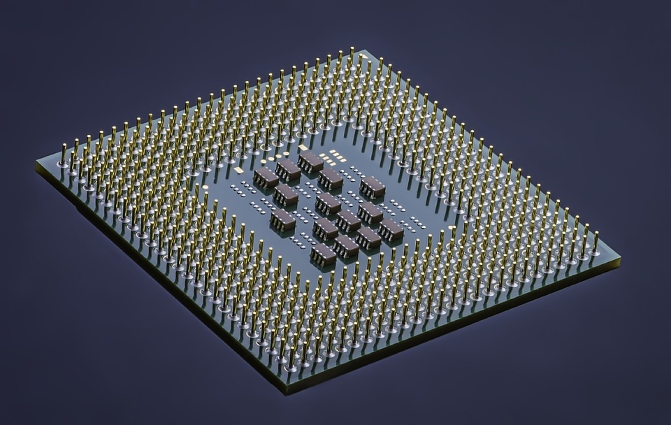
TC While TC is set, DMA operation will be terminated if the contents of the transfer count register becomes zero. The ST/S̅T̅O̅P̅ bit will be reset, if TC is set. If TC bit is cleared, the content of transfer count register in the DMA unit will be decrement for each DMA cycle operation. Although the DMA transfer will not stop when the content of the TC register becomes zero.
SYN: Synchronization bits (2 bits) The operation of synchronization bits is given below:
SOURCE INC Depending B̅/W, on increment source pointer by 1 or 2 after each transfer. If B̅/W = 0, increment source pointer by 1. When B̅/W = 1, increment source pointer by 2.
M/I̅O̅ The source pointer is in M/I̅O̅ space. If M/I̅O̅ is set ( 1 ), the source pointer represents memory. When M/I̅O̅ = 0, the source pointer represents input/output device address.
DEC Depending B̅/W, decrement the source pointer by 1 or 2 after each transfer. If B̅/W = 0, decrement the source pointer by 1. When B̅/W = 1 , decrement the source pointer by 2.
DEST: INC Increment the destination pointer by 1 or 2 after each transfer. When B̅/W = 0, increment the destination pointer by 1. If B/W̅ = 1, increment the destination pointer by 2.
M/I̅O̅ Destination pointer is in M/I̅O̅ space. When M/I̅O̅ is set (1), the destination pointer represents If M/I̅O̅ = 0, the destination pointer represents an input/output device address.
DEC Depending on B̅/W, decrement the destination pointer by 1 or 2 after each DMA data transfer.
P This bit stands for channel priority relative to other channel. Logic level 0 represents low priority and logic level 1 represents high priority. If channels are set at the same priority level, the operation of channels will alternate cycles.
TDRQ If this bit is reset (0), disable DMA requests from the timer 2. When it is set (1) , enable DMA requests from timer 2.
Bit 3 Bit 3 of DMA control register is not used.
Timers:
The 80186 microprocessor has three internal 16-bit programmable timers as depicted in Fig. 11.7. Two of these timers are highly flexible and programmable to count the external events and they are connected to four external pins (2 per timer). These two timers can be used to count external events, time external events, and generate non-repetitive waveforms. The third timer is not connected to any external pins. This timer can be used to interrupt the 80186 after a programmed interval of time to provide a count pulse to DMA unit, real-time coding and time delay applications.
Timer Operation Usually, timers arc controlled by 11 16-bit registers in the internal peripheral control block. The timer control block format is demonstrated in Table 11.2. The count register contains the current value of the tinier and the timer count value can be read or written at any time when the timer is running or not running. The value of this register can be incremented after each timer event, Each of the timers is incorporated with a MAX COUNT register. In general, the MAX COUNT register is used to express the maximum count value of the timer. After reaching the MAX COUNT register value, the timer count value will reset to zero: so that the maximum count value is never stored in the count register itself. A second MAX COUNT register is also present in the timers 0 and 1 . This second MAX COUNT register enables the timers 0 and 1 to swap their count between two different MAX COUNT values which is programmed by the programmer.
As each timer gets a signal on every fourth CPU clock cycle, it can operate at speeds of up to one-quarter the internal clock frequency. External clocking of the timers can be done at the rate of one-quarter of the internal CPU clock rate. When the internal clock frequency is about 8 MHz, the timer operating frequency is 2 MHz. Any timer output can take maximum six clocks to respond to any individual clock or gate input due to internal synchronization and pipelining of the timer circuitry. As the count registers and the maximum count registers are 16 bits wide, 16 bits of resolution are provided in timers. For any read or write operation, the timers will add one wait state to the minimum four-clock bus cycle. This operation is required for synchronization and coordination between the internal timers and the internal bus for the internal data flows. The timers can be programmed in different modes as given below:
- Timer 0, Timer 1 and Timer 2 can be set to halt or continue on a terminal count.
- Timer 0 and Timer 1 can select between internal and external clocks, exchange between MAX COUNT registers and be set to retrigger on external events.
- The timers may be programmed to detect an interrupt on terminal count.
All the above modes of timer operation are selectable through the timer mode/control ward register.
Timer Mode/Control Register Usually, the mode/control register is used to allow the user to program in the specific mode of operation. It is also used to check the current programmed status for any of the three timers. Figure 11.8 shows the timer mode/control register. The operation of tinier mode/control register bits are discussed in this section.
ALT The ALT bit is used to find out which of two MAX COUNT registers is used for count comparison. If ALT is logic level zero, Register A for that timer is always used, while if ALT is logic level one, the comparison will alternate between Register A and Register B when each maximum count is reached. This ALT bit can also be used to determine the function of the timer output pin. If ALT is logic level zero, the output pin will go LOW for one clock, the clock after the maximum count is reached, If ALT is logic level one, the output pin will reflect the current MAX COUNT register being used. Logic level 0 is used for Register B and logic level 1 is used for Register A.
CONT (Count) When the CONT bit is set, the associated timer runs continuously. If the CONT bit is reset, the timer will halt upon maximum count. While CONT = 0 and ALT = 1 , the timer will count to the MAX COUNT Register A value.
EXT (External Bit Selects) This bit selects between internal and external clocking for the timer. When this bit is set, the timer will count low-to-high transitions on the input pin. If it is cleared, it will count an internal clock while using the input pin for control. This external bit signal may be asynchronous with respect to the 80186 clock.
P (Prescaler) The prescaler bit must be ignored when internal clocking is not selected (EXT-0). When the P bit is at logic level zero, the timer will count at one-fourth the internal clock frequency. If the P bit is at logic level one, the output of Timer 2 can be used as a clock for the timer.
RTG (Retrigger) The RTG (Retrigger) bit is only active for internal clocking when EXT = 0. When RTG = 0. the input level gates the internal clock on and off. If the input pin is HIGH, the timer will count otherwise the timer will hold its value. If RTG = 1, the input pin is used to detect the low-to-high transitions. The first such transition starts the timer running, clearing the timer value to zero on the first clock, and subsequently increase. The next transitions on the input pin will again reset the timer to zero, from which it will start counting up again. The input signal may be asynchronous with respect to the 80186 clock.
EN (Enable) The EN (enable) bit gives the programmer control over the timer’s RUN/HALT status. If this bit is set, the timer is always enabled to increment depending upon the input pin constraints in the internal clock mode. When this bit is reset, the timer will be inhibited from counting.
INH (Inhibit) The INH (inhibit) bit is used to allow for selective updating of the EN (enable) bit. If INH is a logic level one while writing to the mode/control word, the state of the EN bit will be modified by the write operation. When INH is a logic level zero during the write, the EN bit will not be affected by the This bit will always be a 0 on a read operation.
INT (Interrupts) When this bit is set, the INT bit enables interrupts from the timer, which will be generated on every terminal count. If this enable bit is reset after the interrupt request has been generated, but before a pending interrupt is serviced, the interrupt request is latched in the Interrupt Controller.
MC (Maximum Count) The MC (Maximum Count) bit is set when the timer reaches its final maximum count value. This bit is set regardless of the timer’s interrupt-enable bit. The MC bit provides information to the programmer about the ability to monitor timer status through software instead of through interrupts.
RIU (Register In Use) The RIU (Register In Use) bit is used to indicate which MAX COUNT register is currently being used for comparison to the timer count value. When RIU = 0, it indicates Register A. The RIU bit cannot be written and its value is not changed when the control register is written. This bit is always cleared when the ALT bit is zero.
Count Registers Each timer has a 16-bit count register. The contents of this register can be read or written by the processor at any time. If we write in the register while the timer is counting, the new value will take effect in the current count cycle.
Max Count Registers Timer 0 and Timer 1 have two MAX COUNT registers, but Timer 2 has a single MAX COUNT register. The MAX COUNT registers are used to store the number of events that the timer will count. In Timer 0 and Timer 1. the MAX COUNT register can exchange between the two maximum count values whenever the current maximum count is reached.
Interrupt Controller:
The 80186 can receive interrupts from both internal and external sources. The internal interrupt controller is able to merge all interrupt requests on a priority basis and provides individual interrupt service by the CPU. Timers and DMA channels are the internal interrupt sources and these sources can be disabled by their own control registers. These can also be disabled by mask bits within the interrupt controller. The 80186 interrupt controller has control registers which can set the mode of operation for the controller.
The interrupt controller can always resolve priority among all pending requests simultaneously. So interrupt service routines for lower priority interrupts might be interrupted by higher priority interrupts. The block diagram of the interrupt controller is shown in Fig. 11.9.
The interrupt controller is able to operate in two different modes such as
- non-iR MX 86 (Master) mode, and
- non-iR MX 86 (Master-Slave) mode.
Non-iRMX (Master) Mode Operation The interrupt controller provides five dedicated pins for external interrupt sources. One of these pins is Nonmaskable Interrupt (NMI). This pin is used for power-fail interrupts, etc.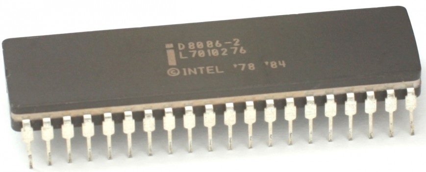 The other four pins may function either as four interrupt input lines with internally generated interrupt vectors, as an interrupt line and an interrupt acknowledge line along with two other input lines with internally generated interrupt vectors. While the interrupt lines are used in cascade mode, the 80186 interrupt controller will not generate internal interrupt vectors. In the cascade mode, external sources use externally generated interrupt vectors. If an interrupt is acknowledged, two INTA cycles are initiated and the vector is used to read into the 80186 on the second cycle. In cascade mode, external 8259A programmable interrupt controllers can be interfaced with the 80186 Microprocessor.
The basic modes of operation of the interrupt controller in non-iRMX mode (Master) are like the 8259A. The interrupt controller responds identically to internal interrupts in all three modes, namely, fully nested mode, cascade mode and special fully nested mode. But the difference of three modes is only in the interpretation of function of the four external interrupt pins. The interrupt controller can be set into one of the three modes after programming the INT0 and INT1 control registers.
Fully Nested Mode In the fully nested mode, four pins are used as direct interrupt requests. The vectors for these four inputs are generated internally. An in-service bit is provided for every interrupt source. If a lower-priority device requests an interrupt while the in-service bit (IS) is set, no interrupt will be generated by the interrupt controller. While interrupts are received and enabled, higher-priority interrupts will be serviced. When a service routine is completed, the proper IS bit must be reset by writing the proper pattern to the EOI register. An EOI command is issued at the end of the service routine just before the issuance of the return from interrupt instruction.
Cascade Mode In cascade mode, the 80186 has four interrupt pins and two of them have dual functions. In the fully nested mode, the four pins are used as direct interrupt inputs and the corresponding vectors are generated internally. In the cascade mode, the four pins are configured into interrupt input-dedicated acknowledge signal pairs. The interconnection between 80186 and 8259A is shown in Fig. 11.10. INT0 is an interrupt input which is used to interface an 8259A and INT2/INTA0 provides the dedicated interrupt acknowledge signal. The same is true for INT1 and INT3/INTA1 . The primary cascade mode allows the capability to serve up to 128 external interrupt sources through the use of external master and slave 8259As. Three levels of priority are created, requiring priority resolution in the 80186 interrupt controller, the 8259A masters, and the 8259A slaves.
Special Fully Nested Mode The interrupt controller operates in this mode after setting the SFNM bit in INT0 or INT1 control register. This mode enables complete nest ability with the external 8259A masters. Usually, any interrupt request from an interrupt source will not be recognized until the in-service bit for that source is reset.
Interrupt Controller Registers The interrupt controller register is depicted in Fig. 11.11. It consists of fifteen registers such as in-service register, interrupt request register, mask register, priority mask register, interrupt status register, timer control register, DMA 0, 1 control registers, INT0-INT3 control registers, poll register, poll status register and EOI register. All registers can both be read or written to unless specified.
iRMX 86 Mode The interrupt controller has a special iRMX 86 compatibility mode that allows the use of the 80186 within the iRMX 86 operating system interrupt structure. This interrupt model requires one master and multiple slaves 8259A in cascade connection. In the iRMX mode, the internal 80186 interrupt controller will he used as a slave controller to an external master interrupt controller. Figure 11.12 shows the iRMX 86 interrupt controller interconnection. The INT0 input is used as the 80186 CPU interrupt input. INT3 functions as an output to send the 80186 slave-interrupt request to one of the eight master PIC inputs. To get correct master-slave interfacing, decoding of slave address CAS0-CAS2 are required. INT1 is used as slave-select input. INT2 is used as an acknowledge output and it is used to drive the INTA input of an 8259A.
The iRMX mode of operation allows nesting of interrupt requests. Vector generation in the iRMX mode is exactly like that of an 8259A slave. In iRMX mode, the specific EOI command operates to reset an in-service bit of a specific priority. All control and command registers such as interrupt vector register, specific EOI register, mask register, priority-level mask register, in-service register, interrupt request register, and Level 0-Level 5 control registers are located inside the internal peripheral control block. Figure 11.13 shows the interrupt controller registers in iRMX86 mode.
Memory Organization:
The 80186 has 20-bit address lines and it can directly address 220 = 1 MB memory. The memory of 80186 is organized in sets of segments. Each segment is available in a linear contiguous sequence of up to 64K bytes. Memory is addressed using a two-component address such as a 16-bit base segment and a 16-bit offset. The 16-bit base values are stored in any one of four internal segment registers: code segment, data segment, stack segment, and extra segment. The physical address is calculated by shifting the base value left by four bits and adding the 16-bit offset value to determine a 20-bit physical address just like the 80186 Microprocessor.
Memory Chip Select The 80186 has six memory chip select outputs for three different address spaces such as upper memory, midrange memory and lower memory. One memory chip select signal is used for upper memory, four memory chip select signals are provided for midrange memory and one memory chip select signal is used for lower memory.
The range for each memory chip select signal is programmable and the range can be set to 1K, 2K, 4K, 8K, 16K, 32K, 64K, 128K and 256K. In addition, the starting or base address of the midrange memory chip select can also be selected. At a time, only one chip select can be programmed to be active for any memory location. Generally, all chip select sizes are in bytes though the memory of 80186 is arranged in words. For example, sixteen 64K x 1 memories are used to develop the 128K memory block.
U̅C̅S̅ (Upper Memory CS) The 80186 provides the upper memory chip select signal U̅C̅S̅ to select the top of memory. Generally, the top of memory is used as the system memory as the 80186 starts executing at memory location FFFF0H after reset. The upper limit of memory is represented by the chip select and it is FFFFFH, but the lower limit is programmable. Actually, the lower limit and the size of the select block can be varied by programming as given in Table 11.3.
M̅C̅S̅ (Mid-range Memory C̅S̅) The 80186 provides four midrange memory chip select signals which are active within a user locatable memory.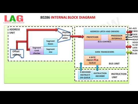 This memory block may be within 1 Mbyte memory address space exclusive the area defined by upper-memory chip-select block and lower-memory chip-select block. The base address and the sum of the select memory block for programming are shown in Table 11.4.
L̅C̅S̅ (Lower Memory) The 80186 provides the lower-memory chip-select signal L̅C̅S̅ to select the bottom of memory. Usually, the bottom of memory is used as the interrupt vector table starting from memory location 00000H. The lower limit of memory is always defined by this chip select and it is 0H. The upper limit and the size of the select memory block can be defined by programming as given in Table 11.5.
Peripheral Chip Selects ln general, the 80186 generates chip-select signals for up to seven peripheral devices. These chip selects are active for seven adjacent blocks of 128 bytes above a programmable base address. This base address can be located in either memory or I/O space. The 80186 generates seven C̅S̅ lines called P̅C̅S̅0-6. The base address is user-programmable but it will be a multiple of 1 k bytes. Therefore, the least significant 10 bits of the starting address are always 0.
Usually P̅C̅S̅5 and P̅C̅S̅6 are programmed to provide latched address bits A1, A2. If these signals are programmed, they cannot be used as peripheral selects. These outputs can be connected directly to the A0, A1 pins and are used to select internal registers of 8-hit peripheral chips. Then the hardware interface becomes simplified as the 8-bit registers of peripherals are simply treated as 16-bit registers located on even boundaries in I/O or memory space. In this case the lower 8-bits of the register are significant, but the upper 8-bits are ‘don’t cares’
The starting address of the peripheral chip-select block can be described by the Peripheral Chip-Select (PACS) register. This register is located at offset A4H in the internal control block. Bits 15-6 of this register correspond to bits 19-10 of the 20-bit Programmable Base Address (PBA) of the peripheral chip-select block. Bits 9-0 of the PBA of the peripheral chip-select block are all zeros. If the chip-select block is located in I/O space. bits 12-15 must be programmed zero, since the I/O address is only 16 bits wide. Table 11.6 shows the address range of each peripheral chip select with respect to the PBA contained in PACS register.
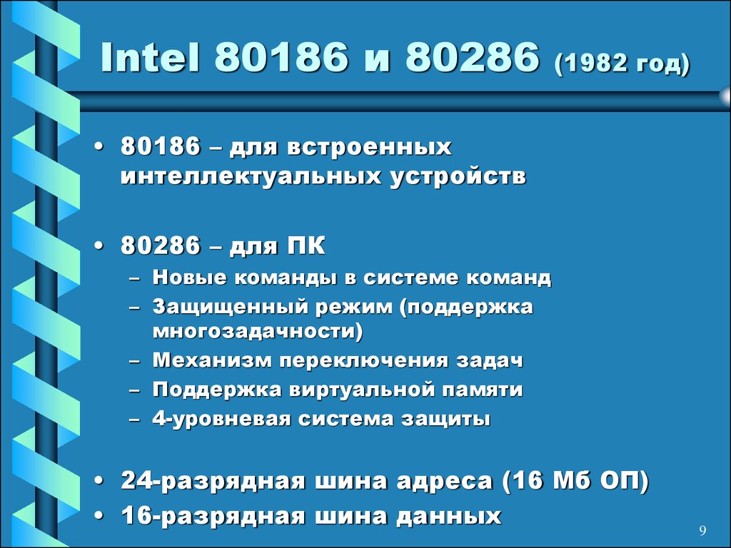
Features of 80186, 80286, 80386 and 80486 Microprocessor
Features of 80186, 80286, 80386 and 80486 Microprocessor:
Let us discuss the Features of 80186 Microprocessor, Features of 80286 Microprocessor, Features of 80386 Microprocessor, Features of 80486 Microprocessor one by one
Features of 80186 Microprocessor:
In 1982, the 80186 microprocessor was developed by Intel. This is an improved 8086 with several common functions built in blocks such as clock generator, system controller, interrupt controller, DMA controller, and timer/counter. This processor has 8 new instructions and executes instructions faster than the 8086. Just like the 8086 processor, it has a 16-bit external data bus. It is also available with an 8-bit external data bus, and then the processor name is 80188 microprocessor. The initial clock frequency of the 80186 and 80188 is about 6 MHz. Generally, these processors are used as embedded processors and also used as the CPU of personal computers.
The second generation of the 80186 family, such as the 80C186/C188 processors, have been developed by Intel in 1987. The 80186 was redesigned as a static, stand-alone module known as the 80C186 Modular Core and its pin configuration is compatible with the 80186 family. The high-performance CHMOS III process allowed the 80C186 to operate at twice the clock rate of the NMOS 80186, but this processor consumes less than one-fourth the power.
The 80C186 Modular Core family was further developed and the 80C186XL processor was developed in 1991. The 80C186XL/C188XL is a higher performance and lower power replacement for the 80C186/C188.
The 80186 and 80188 processor series are generally intended for embedded systems such as modems, public and private PBX switching systems, cellular phones, etc. The architecture of 80186 can also be found in many real-time environments such as robotics, automation industry, measurement control systems, sensors and test equipment’s, fax machines, copiers, printers and medical equipment. Therefore, Intel 80186 processor family, 80186, 80C186XL, 80C186EA/EB/EC, have been accepted in a wide range of applications.
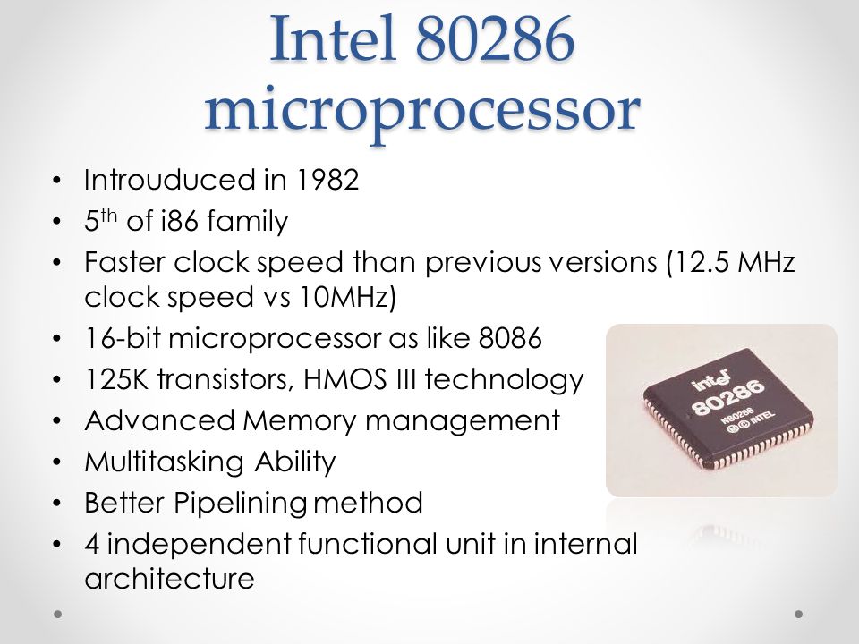
Features of 80286 Microprocessor:
The Intel 80286 was introduced in early 1982. This is also known as iAPX 286 and it is an x86 I6-bit microprocessor with 134,000 transistors. It was the first Intel processor that could run all the software written for its predecessor. It was widely used in IBM PC compatible computers such as IBM PC/AT during the mid 1984 to early 1990s.
Initially, 80286 was released with 6 MHz and 8 MHz, it was subsequently scaled up to 12. 5 MHz. The 80286 had an average speed of about 0.21 instructions per clock. The 6 MHz model usually operated at 0.9 MIPS, the 10 MHz model at 1.5 MIPS, and the 12 MHz model at 1.8 MIPS.
The 80286’s performance is more than twice that of its predecessors, i.e., Intel 8086 and Intel 8088 per clock cycle. The 80286 processors have a 24-bit address bus. Therefore, it is able to address up to 16 MB of RAM, whereas the 8086 could directly access up to 1 MB. The 80286 CPU was designed to run multitasking applications. digital communications, real-time process control systems, and multi-user systems.
This processor is the first x86 processor, which can be used to operate in protected mode. The protected mode enabled up to 16 MB of memory to be addressed by the on-chip linear memory management unit (MMU) with 1 GB logical address space. The memory management unit is able to provide some degree of protection from applications writing outside their allocated memory zones. But the 80286 could not revert to the 8086 compatible real mode without resetting the processor.
80286 is a high-performance 16-bit microprocessor with on-chip memory management and protection capabilities. Actually, this processor has been designed for a multi-user as well as a multitasking system. Usually, the 80286 processor is booted in real mode, and thereafter it works in protected mode by software command. But it is not possible to switch the 80286 from protected mode to real mode. To shift from protected mode to real mode, 80286 microprocessors must be reset. The 80286 with 8 MHz clock provides up to 6 times higher than the 5 MHz 8086.
There is no on-chip clock generator circuit in 80286. Therefore, an external 82284 chip is required to generate the external clock. The 80286 has a single CLK pin for single-phase clock input. Usually, the external clock is divided by 2 internally to generate the internal clock. The 82284 provides the 80286 RESET and READY signals.
The 80286 operates in two different modes such as real mode and protected mode. The real mode is used for compatibility with existing 8086/8088 software base, and the protected mode is used for enhanced system level features such as memory management, multitasking, and protection.
The 80286 is the first advanced microprocessor with memory management and protection abilities.
Features of 80386 Microprocessor:
The concepts of memory management, privilege and protection was introduced with 80286. The 16-bit word length of 80286 provides limitations on its operating speed. But for advanced applications, technology demanded high-speed machines with more powerful instruction sets incorporating all the features of 80286. Subsequently, a CPU with a 32-bit word size and higher operating frequency and high speed of operation, has been developed to overcome all the limitations of 80286. The new processor is called the 80386 processor. This is the third-generation processor and is introduced by Intel in 1985. The Features of 80386 Microprocessor are as follows:
- The 80386 is a 32-bit microprocessor that can support 8-bit, 16-bit and 32-bit operands. It has 32-bits registers, 32-bits internal and external data bus, and 32-bit address bus.
- Due to its 32-bit address bus, the 80386 can address up to 4GB of physical memory. The physical memory of this processor is organized in terms of segments of 4 GB size at maximum.
- The 80386 CPU is able to support 16k number of segments and the total virtual memory space is 4 giga bytes x 16k = 64 terrabytes.
- Another Features of 80386 Microprocessor has a 16-byte prefetch queue.
- It is manufactured by Intel using 0.8-micron CHMOS technology.
- It is available with 275k transistors in a 132-Pin PGA package.
- It operates at clock speeds of 16 MHz to 33 MHz.
- This Features of 80386 Microprocessor has memory management unit with a segmentation unit and a paging Unit.
- It operates in real, protected and virtual real mode. The protected mode of 80386 is fully compatible with 80286.
- The 80386 instruction set is upward compatible with all its predecessors.
- The 80386 can run 8086 applications under a protected mode in its virtual 8086 mode of operation.
- The 80386 processor supports Intel 80387 numeric data processor.
Features of 80486 Microprocessor:
Due to the increasing demand for inure sophisticated processing capability in advanced applications, the 80387 numeric data processors became compulsory for processors. Subsequently, the designers developed a new processor after incorporating the floating-point unit inside the CPU itself. The Intel 80486 is the first processor with an in-built 80387 floating-point unit and it is developed in 1989 using CHMOS IV technology.
The features of the 80486 processor are given below:
- It has complete 32-bit architecture which can support 8-bit, 16-bit and 32-bit data types.
- 8 KB unified level 1 cache for code and data has been added to the CPU. In advanced versions of the 80486 processor, the size of level 1 cache has been increased to 16 KB.
- The 80486 is packaged in a 168-pin grid array package. The 25 MHz, 33 MHz, 50 MHz and 100 MHz ( DX-4) versions of 80486 are available in the market.
- Execution time of instructions is significantly reduced. Load, store and arithmetic instructions are executed in just one cycle when data already exists in the cache.
- Intel 80486 operates at much faster bus transfers.
- This processor retains all complex instruction sets of 80386, and more pipelining has been introduced to improve performance in speed.
- Floating-point unit is integrated with 80486 processor. Hence the delay in communications between the CPU and FPU has been eliminated and all floating-point instructions are executed within very few CPU cycles.
- For fast execution of complex instructions, the 80486 has a five-stage pipeline. Two out of the five stages are used for decoding the complex instructions and the other three stages are used for execution.
- Clock-doubling and clock-tripling technology has been incorporated in faster versions of Intel 80486 CPU. These advanced i486 processors can operate in existing motherboards with 20-33 MHz bus frequency, while running internally at two or three times of bus frequency.
- Power management and System Management Mode (SMM) of 80486 became a standard feature of the processor.
The different variations of 80486 processors are manufactured, but two most common versions are 80486DX with integrated FPU and 80486SX without integrated FPU. The Intel 80486 microprocessor was developed for speeds up to 100 MHz. AMD486 produced at 120 and 133 MHz versions of the 80486, and also manufactured in small quantities the 150 MHz and possibly 166 MHz versions.
|
Processor 80186 For use in various |
|||||||||||||||||||||||||||||||||||||||||||||||||||||||||||||||||
 Processors 80C186/80CI88,
|
⇐ PreviousPage 17 of 34Next ⇒ The 80186 and 80188 microprocessors are similar to, and nearly the same as, the 8086 and 8088 microprocessors, except that they contain a number of built-in controllers. There are four different versions of the 80186/80188 microprocessors, all of which are based on CMOS technology. The 80C186XL and 80C188XL microprocessors are most similar to the base 80186/80188 processors, while the 80C186EC and 80C188EC microprocessors are the most advanced. Microprocessor Basic Block Diagram 80186 6. Note that this block diagram also applies to the 80188 microprocessor, except that the BHE/S7 pin is missing and AD15-AD8 are labeled A15-A8. It should be noted that the internal structure of this microprocessor is slightly more complex than that of the 8088 microprocessor. The block diagrams of the 80186 and 80188 microprocessors are identical, except for the prefetch queue, which is 4 bytes in the 80186 microprocessor and 6 bytes in the 80188 microprocessor. The 80188 microprocessor ( like 8088) has Bus Interface Unit, or otherwise BIU (Bus Interface Unit), and Operation Unit, or EU (Execution Unit).
In addition to the bus interface and operating block, the 80186/80188 microprocessor family has a clock generator, programmable interrupt controller, programmable timers, a programmable DMA controller, and a programmable chip select block. 80286 microprocessor The 80286 microprocessor is an upgraded version of the 8086 microprocessor that has been designed for the multi-user and multi-tasking operating environment. The 80286 microprocessor is capable of addressing 16 MB of physical memory and 1 GB of virtual memory through the use of a memory management system. Currently, the 80286 processor is no longer used in personal computer systems, but sometimes finds use in control systems as an embedded controller.
Hardware features 6.2 shows a block diagram of the 80286 microprocessor. Unlike the 80186/80188 microprocessors, it does not contain built-in controllers. Instead, it contains a memory management unit, otherwise MMU (Memory-Management Unit), which is called the address unit in the block diagram. A review of the block diagram shows that the address pins A23-A0, as well as the BUSY, CAP, ERROR, PEREQ, and PEACK pins, are new or added pins that are not present on the 8086 microprocessor. The signals BUSY , ERROR , PEREQ and PEASK are used when working with a coprocessor, of which the 80287 is an example. The analogous TEST pin of the 8088/8086 processor in the 80286 processor is called BUSY. The 24-bit address bus can address 16 MB of physical memory. The ACS output is connected to a capacitor with a capacity of 0.047 uF + 20% with an operating voltage of 12 V, which in turn is connected to zero potential. The 80286 microprocessor operates in real and protected modes. In real mode, the 80286 microprocessor, using only the 16-bit address bus, addresses only 1 MB of memory and, in essence, is identical to the 8086 microprocessor. In protected mode, the 80286 microprocessor, using all 24 bits, already addresses 16 MB of physical memory.
In addition to the EFLAGS register, the 80286 microprocessor has added a machine status word (MSW) register, a task register (TR), descriptor table registers (GDTR, IDTR, LDTR) and 6 segment register extension registers.
Command system The instruction set of the 80286 microprocessor includes all the instructions of the 8086/8088 processors and has a number of additional instructions. Additional commands control the virtual memory system using the 80286 microprocessor memory control unit. 6.1 lists all of these commands with comments on the purpose of each. Here are only the commands additionally added to the 80286 microprocessor. In addition to them, the 80286 microprocessor command system contains new commands added for 80186/80188 microprocessors, such as: INS, OUTS, BOUND, ENTER, LEAVE, PUSHA, POPA, as well as integer multiplication by a constant and shift commands, including cyclic, with the indication of the counter in a constant. Table 6.1. Additional microprocessor instructions 80286
The following is a description of some of the special commands that are used to manage protection. □ CLTS The CLTS (clear task-switched flag) command clears the TS (task-switched) flag bit in the MSW machine state word register. If the TS flag is set and the next instruction related to the 80287 coprocessor will cause an interrupt (vector type 7). This allows you to programmatically determine if the coprocessor context belongs to the current task. The clts command is used on the system and is considered a privileged command because it can only be executed in protected mode with zero privileges. There is no command to set the TS flag. However, the flag can be set by writing a logical one to bit 3 (TS) of the MSW machine status register using the lmsw command. □ LAR The LAR (load access rights) instruction reads the segment descriptor and places a copy of the access rights byte in a 16-bit register. An example is the LAR instruction ax, in, which loads the AX register with the permission byte from the selected descriptor by the value of the selector specified in the BX register. □ LSL The LSL instruction (load segment limit) loads the segment limit value into a user-allocated register. For example, the LSL instruction ax, in loads into register AX the boundary value of the segment described by the descriptor that is selected by the selector specified in register BX. This command is used to check the limit value of a segment. □ ARPL The ARPL (adjust requested privilege level) command is used to test a selector so that the privilege level of the requested selector is not violated. An example is the ARPL command ax, cx. Register AX contains the requested privilege level, and CX contains the values of the calling process selector to access the handle. If the requested privilege level has a lower priority than the handle being checked, then the zero flag ZF is set. □ VERR The VERR (verify for read access) command checks the segment for readability. This means , that the code segment can be protected from unauthorized reading. If reading from the code segment is enabled, then the zero flag ZF is set; if not, the flag will be cleared. The VERR ax instruction checks the descriptor selected using the AX register. □ VERW The VERW (verify for write access) command checks the segment for write access. The code segment may be protected against unauthorized writing. If writing to the code segment is enabled, then the zero flag ZF is set; if not, the flag will be cleared. Virtual memory The virtual memory machine allows systems with relatively small physical memory (16 MB for the 80286 microprocessor) to map a fairly large area of memory (1 GB for the 80286 processor). Descriptors describe a memory segment only in protected mode. The 80286 microprocessor has descriptors that define codes, data, stack segments, interrupts, procedures, and tasks. The handle is accessed by loading, in protected mode, the segment register by the selector. The selector accesses a handle that describes a region of memory.
⇐ Previous12131415161718192021Next ⇒
See also:
|
 The only difference between the 80186 and 80188 microprocessors themselves is the width of their information buses. The 80186 microprocessor, like the 8086, has a 16-bit data bus, while the 80188 microprocessor and its 8088 predecessor have an 8-bit data bus. The structure of the internal registers of microprocessors 80186/80188 is almost identical to microprocessors 8086/8088. The only difference is that the 80186/80188 microprocessors contain additional spare interrupt vectors and some very powerful built-in I/O capabilities. Microprocessors 80186/80188 are often referred to as embedded controllers (embedded controllers).
  1 is a block diagram of the microprocessor 80188, which, in general, represents all versions.
 :quality(80)/images.vogel.de/vogelonline/bdb/1428900/1428907/original.jpg) These improvements significantly increase the efficiency of the 80186/80188 microprocessors and reduce the number of peripheral components required to implement a computing system. Many popular personal computer subsystems used the 80186 and 80188 microprocessors as a disk controller with cache, controllers local area network (LAN — Local Area Network), etc. Microprocessors 80186/80188 are also used in the cellular telephone network as a switcher. The software of the 80186/80188 microprocessors is identical to the 80286 microprocessor.
These improvements significantly increase the efficiency of the 80186/80188 microprocessors and reduce the number of peripheral components required to implement a computing system. Many popular personal computer subsystems used the 80186 and 80188 microprocessors as a disk controller with cache, controllers local area network (LAN — Local Area Network), etc. Microprocessors 80186/80188 are also used in the cellular telephone network as a switcher. The software of the 80186/80188 microprocessors is identical to the 80286 microprocessor. 
 The capacitor is required for the operation of the internal frequency divider. For comparison, in Fig. Figure 6.3 shows the naming conventions for the 8086 and 80286 microprocessors. It should be noted that the 80286 microprocessor does not have a multiplexed address/data bus.
  6.3. Designation schemes for microprocessors 8086 and 80286
 The command is used to obtain permissions so that it can be checked before programmatic use of the memory segment described by the descriptor.
 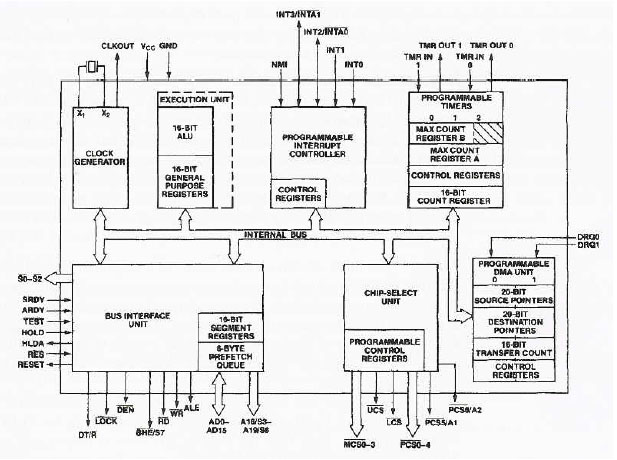 The use of the command ensures that the selector parameter in the routine does not request more privilege than the calling process will allow.
  The very mechanism of virtual memory consists in the fact that an exchange file (swap-file) of several tens of megabytes in size is created on the hard disk, which, in fact, is like an extension of the system’s RAM. During system operation, data and programs are transferred between the exchange file on the hard disk and physical memory as necessary. Addressing virtual memory in the system is carried out using descriptors. Each descriptor (Figure 6.7) of the 80286 processor describes a 64 KB memory segment, and the processor itself has the ability to use 16K descriptors. Thus, this allows the system to have virtual memory up to 1 GB (64 KB x 16K) of virtual memory.
What is Intel 80186 — the meaning of the word, scientific facts — Wikipedia an improved version of the Intel 8086 microprocessor. The new microprocessor includes tools that were previously implemented in 10 separate microcircuits. It was mainly used in work with control applications and in highly intelligent peripheral adapters, such as network adapters.
Microprocessor Intel TR80C186
Intel 80186 microprocessor family architecture
Contents
- 1 Description
- 1.1 New components
- 1.2 Intel 80186
- 1.3 Housing
- 1.4 New instructions
- 1.5 PC based on Intel 80186 family
processor families
- 2 Specifications
- 3 Links
- 4 Notes
Intel began development of the new microprocessor immediately after the release of the Intel 8086/Intel 8088 processors. The Intel 8086 and 8088 processors required a large number of support chips, and Intel decides to develop a microprocessor that already contains all the necessary modules on the chip. The new processor included many components that were previously available as separate chips, which would have made it possible to drastically reduce the number of chips in a computer, and, consequently, reduce its cost. In addition, the system of internal commands (instructions) has been expanded.
New componentsEdit
- Two direct memory access (DMA) controllers with interrupt circuits
- Address Decoders (Programmable Chip Select Circuits)
- Three-channel programmable timer/counter
- Timing generator
- PIC
Intel 80186 processor familiesEdit
In 1982, Intel released the Intel 80186 embedded processor, which, in addition to the improved Intel 8086 core, also contained additional modules that replaced some support chips; The processor was manufactured using NMOS technology.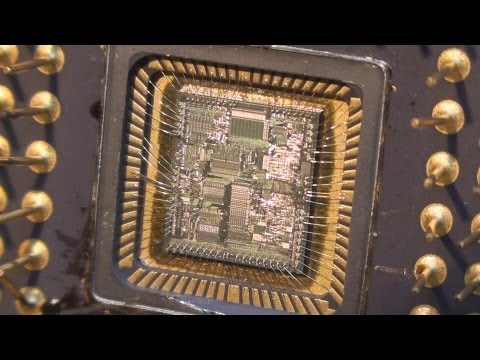
In connection with the development of technology, in 1987, Intel released the second generation Intel 80186 processors — Intel 80C186. These processors were produced according to the improved CHMOS III process technology, which made it possible to double the clock frequency of the processors and reduce the power consumption by 4 times. Importantly, pinout compatibility with older processors has been maintained.
In 1990, Intel released a new family of Intel 80186 processors, the Intel 80C186EB. The new processors contained many changes compared to the previous generation of Intel 80186 processors. First, the processor core was redesigned, which is now modular and was called «80C186 Modular Core» ( 80C186 Modular Core ). Secondly, the family of microprocessor support chips has also been redesigned into modules with standard interfaces. The 80C186EB and original 80186 processors have different support chipsets. In connection with the transition to a new process technology (CHMOS IV) and a modular structure, it was possible to reduce power consumption. The Intel 80C186EB processor has found application in portable equipment (for example, cell phones).
In 1991, Intel introduced the 80C186XL, 80C186EA, and 80C186EC processors, which were also based on the Intel 80C186 modular core. The Intel 80C186XL processor has high performance and low power consumption. The Intel 80C186EA processor combines the Intel 80C186 processor with new power management capabilities. The Intel 80C186EC processor included additional features that other processors in the Intel 80C186 family did not have.
| Features | 80C186XL | 80C186EA | 80C186EB | 80C186EC |
|---|---|---|---|---|
| Extended instruction set 8086 | + | + | + | + |
| Energy saving mode | + | + | — | + |
| Powerdown and Idle modes | — | + | + | + |
| ONCE mode | + | + | + | + |
| Interrupt control unit | + | + | + | + compatible with Intel 8259 |
| + | + | + extended |
+ extended |
|
| DMA 9 module0008 | + 2 channels |
+ 2 channels |
— | + 4 channels |
| Timer control module | — | — | — | + |
| Serial communication module | — | — | + | + |
| I/O ports | — | — | + total 16 |
+ total 22 |
| Year of manufacture | 1991 | 1991 | 1990 | 1991 |
HousingEdit
Due to the increase in the number of components in the processor, the number of pins on the microprocessor package has been increased. The original Intel 80186 processor had 68 pins. The processor was now available in Chip Carrier and Pin Array (PGA) packages. In the next generations of the Intel 80186 processor, other types of packages were used, and the number of contacts increased. To distinguish processors in different types of packages and with different numbers of contacts, identifiers in the form of Latin letters were used, which were placed at the beginning of the processor name (see the table below).
| Processor | Number of pins | Housing type | Identifier | Designation example |
|---|---|---|---|---|
| 80186 | 68 | LCC | R or C | Intel C80186 Intel R80186 |
| 68 | PLCC | N | Intel N80186 | |
| 68 | PGA | A | Intel A80186 | |
| 80C186 | 68 | LCC | R | Intel R80C186 |
| 68 | PLCC | N | Intel N80C186 | |
| 68 | PGA | A | Intel A80C186 | |
| 80 | QFP(EIAJ) | S | Intel S80C186 | |
| 80C186XL | 68 | LCC | R | Intel R80C186XL |
| 68 | PLCC | N | Intel N80C186XL | |
| 68 | PGA | A | Intel A80C186XL | |
| 80 | QFP(EIAJ) | S | Intel S80C186XL | |
| 80 | SQFP | SB | Intel SB80C186XL | |
| 80C186EA | 68 | PLCC | N | Intel N80C186EA |
| 80 | QFP(EIAJ) | S | Intel S80C186EA | |
| 80 | SQFP | SB | Intel SB80C186EA | |
| 80C186EB | 84 | PLCC | N | Intel N80C186EB |
| 80 | QFP(EIAJ) | S | Intel S80C186EB | |
| 80 | SQFP | SB | Intel SB80C186EB | |
| 80C186EC | 100 | PQFP | KU | Intel KU80C186EC |
| 100 | QFP | S | Intel S80C186EC | |
| 100 | SQFP | SB | Intel SB80C186EC |
Notes. 1. There was a sample labeled «Intel A80C186CPICE» in a 280-pin PGA package
(see here).
2. There was an engineering sample marked «Intel FA80C186CP» in a TQFP package with 156 pins
(see here).
New instructionsEdit
The instruction set has been expanded in the Intel 80186 family of processors. Additional commands for working with the stack (PUSHA, POPA, PUSH «immediate»), with I / O ports (INS, OUTS), arithmetic commands (IMUL, ROL / ROR, RCL / RCR, SAL / SAR, SHL / SHR with a directly specified number of shift bits) and commands for implementing high-level languages (ENTER, LEAVE, BOUND).
PCs based on the Intel 80186 family of processorsEdit
Processors of the Intel 80186 family were practically not used in computers, only a few companies released such PCs: Mindset, Compis (Swedish school computer), RM Nimbus (British school computer), Unisys ICON (Canadian school computer), HP 200lx (handheld PC), and the Tandy 2000 desktop PC.
SpecificationsEdit
- Year of announcement: 1982
- Clock frequency, MHz*: 6, 8, 10, 12, 13, 16, 20, 25
- Register width: 16 bits
- Data bus width: 16 bits
- Address bus width: 20 bits
- Addressable memory: 1 MB
- Number of transistors: 55,000
- Manufacturing process, nm: 3000
- Crystal area, sq.