The Intel 8008 support page
Collect and share information and software about Intel’s 8008
— the world’s first 8 bit CPU, introduced April 1972
This site is neither operated nor maintained by
Intel.
Intel is a registered trademark of the Intel Corp, USA
Table of contents
- Preface
- Some history
- General description
- Registers and flags
- Instruction set
- CPU control group
- Input and output group
- jump group
- call and return group
- load group
- arithmetic group
- rotate group
- Pinout
- Pin functions
- The 8008 machine states
- Datasheets
- Identify a 8008
- Vintage computers using the 8008 CPU
- Homebrew computers with 8008 CPU
- Cross-Assembler
- BASIC interpreter
- PL/M compiler
- Simulators and Emulators
- Photo gallery of Intel 8008 chips (on other pages)
- Prices at eBay
- EPROM burner capable of burning Intel 1702A
Preface
When I was searching the web for information about the Intel 8008
a few years ago, little to none information was available. So I
started collecting the bits spread around and began representing
them here.
Meanwhile, the situation has changed. Wikipedia hosts an
excellent article
and a number of scanned datasheets are available.
Special thanks to Klemens Krause,
who maintains a great computer
museum that provided me lots of information and inspiration.
Some history
The Intel 8008 is the world’s first 8 bit microprocessor introduced
in April 1972. The 8008 was originally code named the 1201. The
developers were Ted Hoff, Stan Mazor, Hal Feeney, and Federico Faggin.
Intel designed it for Computer Terminal Corporation (CTC) for use
in it’s Datapoint 2200 terminal, but because the 8008 was delivered too
late and did not meet CTC’s expectations, they didn’t used it. Intel
then brought the rights back and marketed the chip on it’s own.
General description
The Intel 8008 runs at 0.5 MHz, the 8008-1 at 0.8 MHz. It contains
3500 transistors realized in PMOS technology at 10-micron. For
For
comparison, an Intel Pentium 4 consists of 178.000.000 transistors
manufactured in 0.13-micron.
It was used in dumb terminals, general calculators, bottling machines, and for general data/character manipulation.
The 8008 microprocessor contains an accumulator A plus 6 scratch registers B, C, D, E, H and L, each 8 bit wide. H
& L acts as a pointer to memory, providing an virtual register M. This is the only way on the 8008 to access the memory.
Separate from the memory, 8 input ports and 24 output ports can be accessed.
The chip has a 8 bit wide data bus and 14 bit wide address bus,
which can address 16 KB of memory. Since Intel could only manufacture
18 pin DIP packages at 1972, the bus has to be three times multiplexed.
Therefore the chip’s performance is very limited and it requires a lot
external logic to decode all signals.
Very crude interrupt support is given, since the registers can’t be pushed on the hardware stack. If you really need this, you could attach FIFO RAMs
like the SN74LS222 or SN74ALS232 to an I/O port.
Though often heard, it’s not true that the Intel 8008 would be
«twice a Intel 4004» that was introduced one year before. The 4004 has
a harvard architecture and 16 registers while the 8008 has a
von Neumann architecture and 7 registers.
The 8008 family is also referred to as the MCS-8.
Intel 8008 registers and flags
The 8008 microprocessor contains an 8 bit wide accumulator A plus 6
scratch registers B, C, D, E, H and L, each 8 bit wide. H & L acts
as a pointer to memory, providing an virtual register M. This is the
only way on the 8008 to access the memory. H contains the high
significant byte and L the lower significant byte of the 14 bit address.
Sign, Zero, Parity and Carry-flags are available though the 8008 has
no flag register. These four flag bits can be tested with conditional
JMP, CALL and RETurn instructions.
Intel 8008 instruction set
The instruction set of the Intel 8008 can be divided into 7 groups: the CPU control, Input and output, jump, call and return, load, arithmetic and the rotate group.
There are two sets of mnemonics resulting in identically binary
values. The old mnemonics are the first one published at 1972. Intel
changed the mnemonics around the year 1975. Both sets are described
below. The old set is designed to simplify things, it consists of three
characters which can be coded into 16 bits making a lookup-table very
easy.
CPU control group
| binary | old | new | Description |
|---|---|---|---|
| 0 0 0 0 0 0 0 x | HLT | HLT | |
| 1 1 1 1 1 1 1 1 | HLT | HLT |
Input and output group
| binary | old | new | Description |
|---|---|---|---|
| 0 1 0 0 M M M 1 | INP | IN | port MMM |
| 0 1 R R M M M 1 | OUT | OUT | port RRMMM (RR <> 0) |
Jump group
| binary | old | new | Description |
|---|---|---|---|
| 0 1 x x x 1 0 0 | JMP | JMP | unconditionally jump |
| 0 1 0 0 0 0 0 0 | JFC | JNC | JMP if carry = 0 |
| 0 1 0 0 1 0 0 0 | JFZ | JNZ | JMP if result <> 0 |
| 0 1 0 1 0 0 0 0 | JFS | JP | JMP if sign = 0 (positive) |
| 0 1 0 1 1 0 0 0 | JFP | JPO | JMP if parity = odd |
| 0 1 1 0 0 0 0 0 | JC | JC | JMP if carry = 1 |
| 0 1 1 0 1 0 0 0 | JZ | JZ | JMP if result = 0 |
| 0 1 1 1 0 0 0 0 | JS | JM | JMP if sign = 1 (negative) |
| 0 1 1 1 1 0 0 0 | JP | JPE | JMP if parity = even |
Call and return group
| binary | old | new | Description |
|---|---|---|---|
| 0 1 x x x 1 1 0 | CAL | CALL | unconditionally call subroutine |
| 0 1 0 0 0 0 1 0 | CFC | CNC | CALL if carry = 0 |
| 0 1 0 0 1 0 1 0 | CFZ | CNZ | CALL if result <> 0 |
| 0 1 0 1 0 0 1 0 | CFS | CP | CALL if sign = 0 (positive) |
| 0 1 0 1 1 0 1 0 | CFP | CPO | CALL if parity = odd |
| 0 1 1 0 0 0 1 0 | CC | CC | CALL if carry = 1 |
| 0 1 1 0 1 0 1 0 | CZ | CZ | CALL if result = 0 |
| 0 1 1 1 0 0 1 0 | CS | CM | CALL if sign = 1 (negative) |
| 0 1 1 1 1 0 1 0 | CP | CPE | CALL if parity = even |
| 0 0 x x x 1 1 1 | RET | RET | unconditionally return |
| 0 0 0 0 0 0 1 1 | RFC | RNC | RET if carry = 0 |
| 0 0 0 0 1 0 1 1 | RFZ | RNZ | RET if result <> 0 |
| 0 0 0 1 0 0 1 1 | RFS | RP | RET if sign = 0 (positive) |
| 0 0 0 1 1 0 1 1 | RFP | RPO | RET if parity = odd |
| 0 0 1 0 0 0 1 1 | RC | RC | RET if carry = 1 |
| 0 0 1 0 1 0 1 1 | RZ | RZ | RET if result = 0 |
| 0 0 1 1 0 0 1 1 | RS | RM | RET if sign = 1 (negative) |
| 0 0 1 1 1 0 1 1 | RP | RPE | RET if parity = even |
| 0 0 A A A 1 0 1 | RST | RST | call subroutine at adrs AAA000 |
Load group
| binary | old | new | Description |
|---|---|---|---|
| 1 1 D D D S S S | Lds | MOV d,s | load d with content of s |
| 1 1 D D D 1 1 1 | LdM | MOV d,M | load d with content of Mem |
| 1 1 1 1 1 s s s | LMs | MOV M,s | load M with content of s |
| 0 0 d d d 1 1 0 | LdI | MVI d | Load register d with data |
| 0 0 1 1 1 1 1 0 | LMI | MVI M | Load Memory M with data b |
Arithmetic group
| binary | old | new | Description |
|---|---|---|---|
| 1 0 0 0 0 s s s | ADs | ADD s | add contents of s to A |
| 1 0 0 0 0 1 1 1 | ADM | ADD M | add contents of M to A |
| 0 0 0 0 0 1 0 0 | ADI | ADI b | add constant b to A |
| 1 0 0 0 1 s s s | ACs | ADC s | add contents of s + CY to A |
| 1 0 0 0 1 1 1 1 | ACM | ADC M | add contents of M + CY to A |
| 0 0 0 0 1 1 0 0 | ACI | ACI b | add constant b + CY to A |
| 1 0 0 1 0 s s s | SUs | SUB s | sub contents of s from A |
| 1 0 0 1 0 1 1 1 | SUM | SUB M | sub contents of M from A |
| 0 0 0 1 0 1 0 0 | SUI | SUI b | sub constant b from A |
| 1 0 0 1 1 s s s | SBs | SBB s | sub contents of s + CY from A |
| 1 0 0 1 1 1 1 1 | SBM | SBB M | sub contents of M + CY from A |
| 0 0 0 1 1 1 0 0 | SBI | SBI b | sub constant b + CY from A |
| 1 0 1 0 0 s s s | NDs | ANA s | logical AND of s and A to A |
| 1 0 1 0 0 1 1 1 | NDM | ANA M | logical AND of M and A to A |
| 0 0 1 0 0 1 0 0 | NDI | ANI b | logical AND of const b and A to A |
| 1 0 1 0 1 s s s | XRs | XRA s | logical XOR of s and A to A |
| 1 0 1 0 1 1 1 1 | XRM | XRA M | logical XOR of M and A to A |
| 0 0 1 0 1 1 0 0 | XRI | XRI b | logical XOR of const b and A to A |
| 1 0 1 1 0 s s s | ORs | ORA s | logical OR of s and A to A |
| 1 0 1 1 0 1 1 1 | ORM | ORA M | logical OR of M and A to A |
| 0 0 1 1 0 1 0 0 | ORI | ORI b | logical OR of const b and A to A |
| 1 0 1 1 1 s s s | CPs | CMP s | compare s with A, set flags |
| 1 0 1 1 1 1 1 1 | CPM | CMP M | compare M with A, set flags |
| 0 0 1 1 1 1 0 0 | CPI | CPI b | compare const b with A, set flags |
| 0 0 d d d 0 0 0 | INd | INR d | increment register d (d<>A) |
| 0 0 d d d 0 0 1 | DCd | DCR r | decrement register d (d<>A) |
Rotate group
| binary | old | new | Description |
|---|---|---|---|
| 0 0 0 0 0 0 1 0 | RLC | RLC | rotate content of A left |
| 0 0 0 0 1 0 1 0 | RRC | RRC | rotate content of A right |
| 0 0 0 1 0 0 1 0 | RAL | RAL | rotate content of A left through CY |
| 0 0 0 1 1 0 1 0 | RAR | RAR | rotate content of A right through CY |
Each I-instruction (immediate addressing mode) is followed by a second byte containing the data.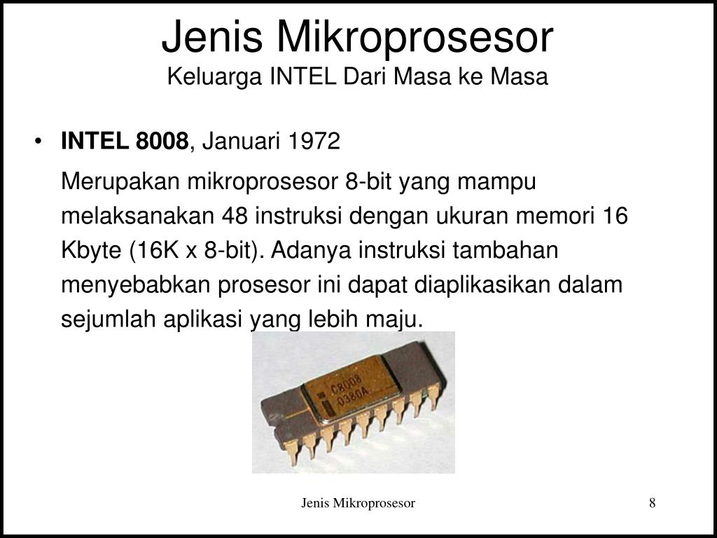
Each JMP- and CALL-instructions are followed by two bytes containing
the address. The LSB follows first, then the MSB. Since the 8008 uses
only 14 address lines, the most significant two bits are ignored.
Intel 8008 pinout
                        ____    ____
		      _|    \__/    |_
	     --> Vdd |_|1         18|_| Interrupt <--
		      _|            |_
	     <--> D7 |_|2         17|_| Ready <--
		      _|            |_
	     <--> D6 |_|3         16|_| Phase 1 <--
		      _|            |_
	     <--> D5 |_|4  Intel  15|_| Phase 2 <--
		      _|            |_
	     <--> D4 |_|5  8008   14|_| Sync  -->
		      _|            |_
	     <--> D3 |_|6         13|_| S0 -->
		      _|            |_
	     <--> D2 |_|7         12|_| S1 -->
		      _|            |_
	     <--> D1 |_|8         11|_| S2 -->
		      _|            |_
	     <--> D0 |_|9         10|_| Vcc <--
		       |____________|
Pin functions
| D0-D7 | bi-directional address/data-bus. |
| Interrupt | (input, active high). Interrupt request is generated by I/O devices. |
| Ready | (input, active high). If pulled to Low, the CPU waits for slow memory. |
| Phase 1, Phase 2 | (input). Two-phase clock, non-overlapping. The microprocessor needs this to generate a four-phase-clock internally. |
| Sync | (output, active high). Indicates that the current machine cycle is the opcode fetch cycle of an instruction execution |
| S0-S2 | (output, active high). Machine status-signals, described below |
| Vdd, Vcc | Provide -9V at Vdd and +5V at Vcc to operate at TTL-levels |
The 8008 machine states:
| Name | S2 | S1 | S0 | Function |
|---|---|---|---|---|
| wait | 0 | 0 | 0 | Wait for slow memory |
| T3 | 0 | 0 | 1 | Data input/output (memory access) |
| T1 | 0 | 1 | 0 | Less significant address byte |
| stop | 0 | 1 | 1 | Wait for interrupt (HLT) |
| T2 | 1 | 0 | 0 | More significant address byte + cc2 + cc1 |
| T5 | 1 | 0 | 1 | Internal data transfer |
| T1I | 1 | 1 | 0 | Like T1, but interrupt recognized |
| T4 | 1 | 1 | 1 | Internal data transfer |
cc2 and cc1 provided at T2-state give more information about the T3-state:
| Name | cc2 | cc1 | Function |
|---|---|---|---|
| PCI | 0 | 0 | Instruction Cycle.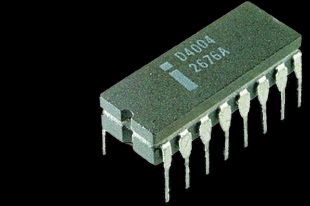 The first byte (containing the opcode) is read from the memory The first byte (containing the opcode) is read from the memory |
| PCR | 1 | 0 | Read Cycle. Data or following parts of the opcode are read from the memory |
| PCC | 0 | 1 | Command Cycle. Input-Output-Instruction. Whether a byte shall be read or written depends on the address |
| PCW | 1 | 1 | Write Cycle. Write data to memory |
Datasheets
- MCS-8 at bitsavers
- Various documents are at
Bryan’s Old Computers and at the bottom of
8008chron.com.
Identify a 8008
The part’s name varies depending on the manufacturer.
-
Intel
D8008-1 e.g. lets you know:
- Package type
- C = Side-brazed ceramic DIP
- D = ceramic DIP
- P = Plastic DIP
- Part number 8008
- Frequency
- blank = 0.5 MHz
- -1 = 0.8 MHz
- Package type
-
Microsystems International
MF8008R = 0.
 5 MHz, MF8008-1R = 0.8 MHz, 18-pin ceramic DIP,
Gray ceramic/gold top/gold pins — no further information available. -
8008 by Siemens
SAB8008-1C = 0.8 MHz, 18-pin ceramic DIP, Purple ceramic/gold top/gold pins- no further information available.
-
Clones by east german VEB Funkwerk Erfurt
The equivalent name is U808D or VB808D for the military version, both running at 0.5 MHz — no further information available.
Vintage computers
Some early designs used the 8008. Follow the external links to get more informations about these computers.
- Mark-8
- The Mark-8 at oldcomputers.com
- Mark-8 Minicomputer
- A Mark-8 Experience
The Mark-8 Minicomputer
- MCM 70/700
- The Micro Computer Machines MCM/70
- MCM Model 782 APL
- NBI Hantu
- R2E Micral
- Robotron K 1510 / PBT 4000
- Robotron PBT4000, robotrontechnik.
 de (German)
 - Robotron K1510, Museum FH-Brandenburg (German)
- Robotron PBT4000, robotrontechnik.
- Scelbi 8H, Scelbi 8B
- SCELBI Computer Museum
- Scelbi 8H, Scelbi 8B
- The 8008 and Scelbi
SCELBI’s Wikipedia page
- MIL MOD-8 and GNC-8
- Bill-1 by Litton Data Systems
Homebrew Computers
- emuf08 (German)
- 8008 Computer «Clock»
SCELBI 2002LC-8008
Cross Assemblers
- The
Macroassembler AS by Alfred Arnold has been my favorite assembler for
many years. It’s latest version supports the 8008 now, with both old and new
instruction sets. AS is available for almost any platform a C compiler exists
for. - SB-Assembler is a free cross-assembler supporting a lot of CPUs including the 8008
- AS8 by
Thomas E. Jones is a small 8008 Assembler written in ANSI-C, source code is
available, as well as a Windows executable. The original web pages
The Mark-8 MinicomputerandAS8 User’s Manualare offline.
BASIC interpreter
- SCELBAL is a BASIC interpreter written in assembler, published by
SCELBI COMPUTER Consulting, Inc.
8008chron.com hosts another version of the code.
PL/M for the Intel 8008
- Gary Kildall programmed a PL/I
compiler for the 8008 in FORTRAN and called it
PL/M.
I wish, that compiler would appear somewhere…
Simulators and Emulators
- SIMH, emulates a lot of historic computers including a SCELBI-8B
- 8008 Simulation In JavaScript running SCELBAL
- Semi-Decent 8008 Emulator
- 8008/SCELBI OS/X Emulator Program
- Sim8008 by Andreas Gebhardt, Simulator with assembler and
debugger for Windows, in German only
Photo gallery of Intel 8008 chips (on other pages)
- cpu-zone.com — watch’em all! 😉
- cpu-world.
 com
com - cpu-collection.de
- Ken Shirriff’s blog — Die photos and analysis
Prices at eBay
| Date | Price | Location | Description |
|---|---|---|---|
| 2005-11-07 | US $123.50 | Silverdale, WA, USA | Intel C8008, date code 76xx |
| 2005-11-06 | EUR 24.17 | Trier, Germany | MF8008R, military version by Microsystems International, date code 7439 |
| 2005-10-31 | EUR 26.50 | Germany | U808 by MME, NOS, yellow and green marking, east german clone |
| 2005-10-01 | US $61.66 | Bouvancourt, France | Intel C8008 CPU, date code 7512, Malaysia, NOS |
| 2005-09-29 | US $60.00 | Newmarket (Toronto), Canada | Intel C8008 Processor, date code 7619, Philippines, grey ceramic DUP, one of the end pins broken, some scratches on the top |
| 2005-09-08 | US $188. 50 50 |
Vermont, USA | Intel 8008-1, gold plated ceramic DIP |
| 2005-09-02 | US $47.23 | APO, AP, USA | Intel C8008-1, date code 7701, Malaysia, guaranteed of being in excellent condition, authentic and functioning |
| 2005-09-02 | US $42.00 | APO, AP, USA | Intel C8008, date code 7729, Hong Kong, guaranteed of being in excellent condition, authentic and functioning |
| 2005-08-03 | US $44.77 | Ottawa, ON, Canada | Intel C8008-1, Malaysia 1977, date code 7701, out of some ancient HP lab equipment (02640-60008) |
| 2005-08-03 | US $56.55 | Ottawa, ON, Canada | Intel C8008-1, Phillipines 1976, date code 7640, out of some ancient HP lab equipment (02640-60008) |
| 2005-08-02 | US $46.00 | Newmarket (Toronto), Canada | Intel C8008, grey ceramic DIP with gold leads, date code 7730, Hong Kong, pin 9 missing, part of the ceramic has chipped away |
| 2005-07-08 | US $57. 00 00 |
APO, AP, USA | Intel C8008-1 3157A, date code 7705, Malaysia, NOS |
| 2005-07-08 | US $103.50 | APO, AP, USA | Intel C8008 03398, date code 7740, Malaysia, NOS |
| 2005-07-04 | EUR 36.50 | Fohrde, Germany | U808D by MME, east german clone |
| 2005-06-26 | US $55.57 | Brighton, Michigan, USA | Intel 8008-1 |
EPROM burner for Intel 1702A
The very first 8 bit CPU often ran its programs off the very first
EPROMs: the Intel 1702 and Intel 1702A, each holding 256 Bytes.
They are very different compared to later, more common EPROMs so that it’s
very hard to find a programmer these days, that is capable of burning
these beasts:
- Simple 1702A EPROM Programmer by Stephen H. Lafferty
Martin Feberhard designed a new EPROM burner based on a modern
microcontroller: MFeberhard 1702A Programmer. Have a look at the Yahoo group
Altair Computer Club.
Happy 50th Birthday to the 8-bit Intel 8008 Microprocessor – EEJournal
Early microprocessors straddled two major computing epochs. During the first epoch, stretching from the late 1960s through the 1970s, computer system engineers designed and implemented minicomputer processor architectures and processor boards using TTL parts, bipolar PROMs, stone knives, and bearskins. Each minicomputer maker – including Digital Equipment Corp (DEC), Data General (DG), Prime, Computer Automation, IBM, Burroughs, HP, Four-Phase, NCR, and Univac – had their own, proprietary minicomputer architectures, ISAs, and dedicated peripherals. It was the wild, wild West. During the second epoch, which partially overlapped the first epoch, some computer manufacturers and some semiconductor vendors started designing LSI chips with increasingly large processor chunks integrated onto an IC, culminating in the development of single-chip microprocessors.
The first commercially successful, single-chip microprocessor – an early child of the second epoch – was the 4-bit Intel 4004, which just celebrated its 50th birthday on November 15, 2021. (See “Say Happy 50th Birthday to the Microprocessor, Part I” and “Say Happy 50th Birthday to the Microprocessor, Part 2.”) The 4004 microprocessor arrived with much hoopla, but Intel had a second microprocessor in development at the same time. That microprocessor was the 8-bit Intel 8008. The stories of these two processors intertwine in many ways, and they’re independent in others.
Like the Intel 4004 microprocessor, an external customer drove the development of the Intel 8008 microprocessor. For the Intel 4004 microprocessor, the external customer was Busicom, a Japanese calculator company that wanted the Intel 4004 to build high-end desk calculators. Intel designed and built the 4004 and three companion chips for Busicom and then later negotiated the right to market the Intel 4004 microprocessor to other companies, in exchange for price concessions made to Busicom on the parts. Intel introduced the 4004 microprocessor to the world on November 15, 1971.
The 4-bit Intel 4004 microprocessor was part of a 4-chip set, including the microprocessor, a ROM, a RAM, and a shift register for I/O expansion. This 4-chip set, dubbed the Intel MCS-4, represented a walled garden. The microprocessor’s unique, multiplexed, 4-bit bus formed the garden wall. If another chip wanted to communicate with the Intel 4004 microprocessor, it had to implement the control and timing logic needed to interface with that multiplexed bus.
At the time, Intel’s primary business was selling memory, specifically RAMs and ROMs. These memories all had parallel address and data buses. None were directly compatible with the Intel 4004’s unique bus. That was not the vision for the Intel 8008 microprocessor, which was developed with a simpler system bus in mind. The 8008 was designed to use standard RAMs and ROMs, which Intel was making as well.
The external customer for the Intel 8008 was the Computer Terminal Corp (CTC), located in San Antonio, Texas. CTC made an outsized contribution to the Intel 8008 microprocessor’s architecture and ISA. The microprocessor’s definition was based on CTC’s existing plans for an 8-bit, board-level processor built with about 100 SSI and MSI TTL chips. Using their experience with the 4004’s development, Ted Hoff and Stan Mazor at Intel reviewed and tweaked CTC’s planned processor architecture slightly to improve it, to ease its manufacture as a single chip, and to allow Intel to cram the microprocessor into an itty-bitty 18-pin DIP. The architectural tweaks involved changes to the ISA.
CTC made dumb terminals, and Intel was supplying a custom, 512-bit recirculating shift register for that application. CTC wanted to expand into the growing minicomputer terminal business, and it was developing an 8-bit embedded processor board as the foundation for an intelligent terminal that it planned to make. As part of that development, CTC’s Technical Director, Victor Poor, investigated Intel’s 64-bit (NOT Kbit or Mbit) bipolar SRAM as a possible way to implement the CTC processor’s registers. He asked Intel if it could make a custom version of the SRAM by adding a counter to the RAM design, enabling its use as a pushdown stack register.
Intel’s Stan Mazor, who’d worked on the early definition of the Intel 4004, discussed the requirements with Poor, developed a deeper understanding of the CTC processor architecture, and then wrote three proposals for custom chips. Mazor’s first proposal was for an 8-bit register set with a stack counter, per Poor’s initial request. The second proposed chip was a register stack with an added arithmetic unit (conceptually similar to the Four-Phase AL1). The third proposal was for an entire 8-bit CTC CPU on one chip. That one got Poor’s attention.
Mazor didn’t even have a detailed description of the CTC processor architecture or its ISA when he created this proposal, but Poor was sufficiently intrigued by the third proposal to send Mazor the programming manual for the processor, which described the architecture at the assembly-language level. Mazor and Ted Hoff, freshly freed from the Intel 4004 project (and leaving Federico Faggin to develop and sweat over the silicon-gate process and logic implementation details), studied the CTC processor’s programming manual in depth and created a more detailed proposal for a single-chip version of CTC’s 8-bit CPU processor. The Intel salesperson for CTC then got involved, and CTC cut a $3 million purchase order for the one-chip processor on March 18, 1970 for 100,000 parts at $30 apiece. (To see an image of this purchase order, check out Lamont Woods’s article titled “Digital World’s Birth Certificate Written in San Antonio.”)
Freshly hired Hal Feeney became the chip designer for the 8-bit processor project. Mazor and Feeney started their development with the proposal Intel provided to CTC. However, the project quickly went on hiatus because there was some question as to whether CTC was really committed to the development of this custom chip. (A pause of similar duration had occurred in the development of the Intel 4004, but there the fault was entirely Intel’s.) With the 8-bit microprocessor project stalled, Feeney went off to help Federico Faggin finish development of the 4004 microprocessor and the MCS-4 chipset.
There is something very interesting about the detailed microprocessor proposal that Intel sent to CTC. The proposal accidentally contained a design flaw that would prevent the microprocessor from properly servicing interrupts. As originally defined, the interrupt mechanism would cause the microprocessor to call the interrupt service routine without first putting the return address onto the processor’s stack, so there was no way for the interrupt service routine to return from the interrupt. This flaw made the proposed interrupt mechanism useless.
Around this time, Texas instruments (TI) also started developing a single-chip processor for CTC, based on CTC’s specification and at CTC’s request. TI’s processor would be called the TMX 1795. Although TI originally proposed a 3-chip set for CTC’s processor, it switched to a single-chip design sometime after Intel made its own proposal to CTC. TI built the TMX 1795 on a very large die, which would not have been economical to produce in volume. In addition, according to Feeney, darned if the TMX 1795 didn’t have an identical interrupt design flaw that worked just the way that Intel had mistakenly defined it.
TI built the TMX 1795 but didn’t succeed in selling it to CTC and never successfully marketed the device. Instead, TI went off and successfully sold tons of TTL, calculator, and other chips. The TMX 1795 microprocessor survives in stories and as a few artifacts, including a 1996 video of the device in operation, at the Computer History Museum in Mountain View, California. (For more details about this little-known TI microprocessor, see Ken Shirriff’s blog titled “The Texas Instruments TMX 1795: the (almost) first, forgotten microprocessor.”)
Meanwhile, the 8008 microprocessor’s 6-month project hiatus actually helped Intel debug and improve the design. First, it provided time to reflect on and refine the 8-bit processor’s architecture. The original CTC instruction set included a branch-on-bit instruction. The Intel design team determined that the instruction wasn’t needed and removed it to simplify the processor’s hardware design. At the same time, the Intel design team determined that the processor would greatly benefit from increment and decrement instructions, so they added these two instructions to the 8008’s ISA. The hiatus also allowed the Intel 8008 design team to catch and fix the flawed interrupt mechanism.
In addition, the hiatus provided time for Intel’s breakthrough 1103 1Kbit DRAM to go into production. That was a significant event for many reasons, but the direct benefit to the 8008 project was the 18-pin DIP that housed the first high-volume DRAM. Because that package was now officially sanctioned by Intel’s production group, the Intel 8008 design team could use it to add two more precious pins to the Intel 8008. Previously, the 8008 design team had been restricted to 16 pins, because that was the package that Intel’s production group had on hand.
According to Feeney, those two extra pins were sorely needed to improve the 8-bit processor. Among the benefits: one of the extra pins was used to bring additional state information out of the microprocessor, which helped to implement the microprocessor’s stack and allowed the interrupt mechanism to work properly.
The Intel 8080 Microprocessor was packaged in an 18-pin DIP, which Intel also used for its 1103 1Kbit DRAM. Photo Credit: CPU Collection Konstantin Lanzet
With careful design and Faggin’s semiconductor process and design methodology improvements, some of which he’d developed for Intel’s MCS-4 project, Feeney’s 8008 microprocessor die was only slightly larger than the Intel 4004 microprocessor die, even though the 8008 needed 50 percent more transistors count (3500 transistors versus 2200 for the 4004). Feeney’s design was therefore quite manufacturable. Unfortunately, the Intel 8008 microprocessor, implemented in silicon-gate MOS, ran significantly slower than the bit-serial TTL version of the processor that CTC had designed and implemented. It also required a significant number of support chips to create a complete system, although not as many as the 100 chips on CTC’s processor board, so the savings in chip count when using the 8008 microprocessor weren’t quite as significant as they might have been.
CTC evaluated the Intel 8008 microprocessor in late 1971, and said, “No thanks.” It was too little, too late. The company had already developed its first Datapoint 2200 terminal with the bit-serial TTL processor and was working on an even faster parallel implementation for the next generation of terminals. CTC sold Datapoint 2200 machines until 1979 and upgraded the TTL processor board’s design several times along the way. The TTL processor became faster with each revision.
Datapoint 2200 Intelligent Terminal with a removable, 2. 5Mbyte hard disk cartridge sitting on top. Photo Credit: www.engcyclopedia.de
The Datapoint 2200 terminal was much more than a terminal. It was a minicomputer that you could program in BASIC or PL/B and was offered with one or two digital cassette tape drives, a companion 2.5Mbyte hard disk drive, and later, with an optional floppy disk drive. Some historians have called it the first personal computer, and it was clearly designed to be a computer, but it wasn’t based on a microprocessor. It merely spawned one. CTC’s Datapoint 2200 intelligent computer/terminal sold so well that the company later changed its name to Datapoint.
Meanwhile, having lost its main customer, Intel now owned the rights to the 8008 microprocessor and decided to sell it commercially. Although many online articles and references use April, 1972 as the introduction date for the Intel 8008, the company announced the microprocessor on March 13, 1972, just four months after announcing the Intel 4004. A few online citations say it was 1974, obviously confusing the Intel 8008 and 8080 microprocessors. However, thanks to Ken Shirriff’s extensive research, the Intel 8008’s formal debut appears to have been a 1-page article, written by Stephen William Fields and titled “8-bit parallel processor offered on a single chip,” which appeared in the March 13, 1972 issue of Electronics magazine (See Note 2 below.)
Intel was now selling not one but two single-chip microprocessors: the 4004 and the 8008. They had a clear lead in this new market.
The Intel 8008 microprocessor has a 16Kbyte address space (using 14-bit addressing, considered immense at the time, and four times larger than the 4004 microprocessor), and a two-phase, 800KHz clock (for the fastest speed grade). According to the data sheet, an 8008 instruction fetch/execute cycle requires a minimum of five processor states, or 10 clocks. That’s a peak instruction execution rate of 80,000 instructions per second.
If measured by today’s microprocessor standards, or even by the standards of 30 years past, Intel’s 8008 is truly feeble and slow. But it was the first commercial, 8-bit, single-chip microprocessor, and you could build useful systems with it. System designers started to incorporate the Intel 8008 into many new products including embedded systems, such as the first two versions of HP’s legendary and long-lived 2640 series smart CRT terminals (take that, CTC!), and several early microcomputers. In addition, the 8008 microprocessor’s introduction helped Intel sell a lot more of its main products, namely DRAMs and EPROMs, by enabling and even encouraging the design of systems that needed semiconductor memory.
The Intel 8080 and 8085, the 8-bit Zilog Z80, and all x86 microprocessors developed over the last half century by Intel and other processor vendors all carry some reptilian DNA from the original Intel 8008. If you don’t believe that, just look closely at the register sets in these microprocessors.
That’s quite a legacy, wouldn’t you agree?
Notes:
- Federico Faggin left Intel and founded Zilog in 1974.
 He put some 8008 microprocessor DNA into the extremely successful 8-bit Z80 microprocessor, which Zilog announced in 1975. But that’s another story, for another time.
 - For an excellent and detailed analysis of the Intel 8008 microprocessor’s design, see Ken Shirriff’s blog titled “Die photos and analysis of the revolutionary 8008 microprocessor, 45 years old.”
- To see the article announcing the 8008 microprocessor in the March 13, 1972 issue of Electronics magazine, see Ken Sirriff’s blog titled “Analyzing the vintage 8008 processor from die photos: its unusual counters,” and scroll down to the “Notes and References” section. There’s an image of the one-page article there. Read the blog along the way, of course, because it’s filled with interesting facts. For example, Shirriff’s reverse engineering shows how and why Intel implemented the 8008 register set using DRAM cells instead of latches (to save transistors).
References:
Oral History Panel on the Development and Promotion of the Intel 8008 Microprocessor, Computer History Museum, September 21, 2006.
Lamont Wood, Datapoint: The Lost Story of the Texans Who Invented the Personal Computer Revolution, Hugo House Publishers, 2012.
Intel 8008 processor — what’s inside? / Habr
It’s hard to believe, but the Intel 8008 processor, the first of its kind, the forerunner of the giant x86 processor family, was born exactly 45 years ago — on April 1, 1972. The story of his birth, as you know, was quite confusing and, for sure, at that time few people saw him as a future legend. Well, now the steepness and grandeur of 8008, I think, few will dispute — it was really a milestone in chip building. With the help of oldfag enthusiast Ken Shirriff and his microscope, let’s take a look inside this chip and see how it works.
Here is the crystal of the 8008 processor in all its glory. The squares on the sides are platforms to which massive legs were soldered. On the chip, you see «8008» on the right and «Intel 1971» on the bottom. The initials HF on the top right belong to Hal Feeney , who created the logical and physical circuitry of the processor. Together with Fini, Ted Hoff, Stan Mazor and Federico Faggin worked on the creation of 8008.
Let’s now consider the constituent functional parts of our chip. On the left we see Arithmetic/Logic Unit (ALU) performing calculations on the available data. The ALU has two temporary registers for storing input data. As we can see, they are large in size, but not because of the complexity of the device, but because of the size of the transistors used in them.
Below are the preview elements in the Carry scheme. When adding and subtracting, this component calculated all 8 carry values in parallel to improve performance. Since the carry of the least significant bits depends only on the least significant bits, while for the most significant ones it depends on different bits, this circuit block has a triangular shape.
ALU’s triangular shape is unusual. It usually has the shape of a rectangle (bitwise structure). In the 8008, however, 8 blocks (one per bit) are randomly arranged to fit the carry generator triangle.
In the center of the chip is an instruction register and an instruction decoding circuit that determines the value of each 8-bit instruction. Decoding is carried out using the Programmable Logic Array (PLA) , which, when certain bit sequences are found, generates the appropriate control signals for the entire chip. On the top right, we see 7 storage registers, below them is an address stack consisting of eight 14-bit address words. Unlike most processors, the 8008’s call stack is stored directly on the chip, not in memory.
What layers does our crystal consist of? To answer this question, let’s make the increase even stronger. Now we see 3 layers: the topmost is a metallic electrically conductive one. Under it is a layer of polycrystalline silicon, under a microscope it has an orange color. Even deeper is a gray silicon substrate with dopant particles forming a semiconductor. The substrate is difficult to see, but black lines can be seen between pure silicon and doped silicon.
Now let’s see how the power bus (blue and red lines) and the data bus (rainbow line) were located on the chip. The data bus connects the ALU on the right to the instruction register, holding register, and address stack on the right. Power distribution proved to be a challenge as well. The first microprocessors had only one metal layer, and it had to be arranged in such a way that there were no shorting crossovers.
And this is what the register set of the 8008 processor looks like. It consists of an array of 8×7 DRAM cells, each of which uses 3 transistors to store one bit. Each row is one of seven 8-bit registers (A, B, C, D, E, H, L). On the left you see the horizontal read and write select lines, on top the vertical read and write bit lines and the power lines. The use of DRAM in registers instead of static flip-flops is also unusual. This is probably due to the fact that Intel, which originally dealt with memory, had more experience with DRAM.
Something about the Intel 8008 may seem primitive, if not dubious. Like all devices in the world, the processor was not without flaws, some of which were already visible then. Say, for technically inexplicable reasons, the 8008 had only 18 legs, and the transfer of a full set of data and address bits took as much as 3 I / O cycles. The problem was obvious, and the next processor, the i8080, already had 40 pins. But, on the other hand, do not forget: 45 years have already passed. This is a lot from a human point of view, and even by the standards of processors, it’s just a distance of a galactic size. From these positions, let’s look at this remarkable product.
Intel 8008 | it’s… What is the Intel 8008?
The Intel 8008 is the first 8-bit CPU developed by Intel Corp. and released April 1, 1972. The processor was positioned as a processor for advanced general purpose calculators, input/output terminals, and bottling machines.
Contents
|
History
In 1969, Computer Terminal Corporation (CTC), later renamed Datapoint, orders a new processor from Intel, which CTC intended to integrate into the new Datapoint 2000 terminal. Intel — Ted Hoff, looking at the project, proposed to place all the components of the new processor on a single chip. With the consent of the CTC, Intel engineers began to develop a chip, which received the working name 1201. At 1970, when the chip was almost ready, CTC abandons the project. The reasons were as follows — the chip was provided late, and the characteristics of the chip did not satisfy CTC, as a result, it was not used in Datapoint 2200 terminals. The contract between Intel and CTC was broken, which allowed selling this chip to other companies. Chip 1210 became interested in the Japanese company Seiko. Subsequently, after some modification, 1210 turned into the i8008 microprocessor (released in 1972), which laid the foundation for the new MCS-8 family.
The i8008 microprocessor was architecturally very similar to the i4004, many of the solutions used in the i4004 were also used in the i8008. The new processor also inherited the notation used in the 4004, similarly, the 8xxx product family included all RAM, ROM and EPROM chips that support the microprocessor 8008.
Description
- 14-bit memory addressing, as a result of which the processor could support up to 16K bytes of external memory,
- 8-bit bus,
- processor could access 8 input ports and 24 output ports.

The