intel%208748%20microcomputer datasheet & applicatoin notes
Top Results (6)
| Part | ECAD Model | Manufacturer | Description | Datasheet Download | Buy Part |
|---|---|---|---|---|---|
| PMP5486 |
Texas Instruments |
Sync Buck for Intel IMVP6+ Atom | |||
| PMP5800 |
Texas Instruments |
Sync Buck (1.05V @ 48A) for Intel X86 | |||
| PMP5783.1 |
Texas Instruments |
Synchronous Buck for Intel Core i3, i5, i7 Arrandale SV (1. |
|||
| PMP5885.2 |
Texas Instruments |
Sync Buck for Intel Celeron M723 (1.05V @ 15A) | |||
| PMP5922.6 |
Texas Instruments |
Sync Buck for Intel Atom E6xx Tunnel Creek (2.5V @ 50mA) | |||
| PMP5922.9 |
Texas Instruments |
Sync Buck for Intel Atom E6xx Tunnel Creek (1.25V @ 10mA) |
intel%208748%20microcomputer Datasheets Context Search
| Catalog Datasheet | MFG & Type | Document Tags | |
|---|---|---|---|
2009 — AF82801JIB
Abstract: AF82801 intel ICh20 AC82G45 E7400 X4500 Q9400 E6500 intel e5300 E8400 |
Original |
|
82G45 1209/KSC/OCG/XX/PDF 321387-003US AF82801JIB AF82801 intel ICh20 AC82G45 E7400 X4500 Q9400 E6500 intel e5300 E8400 |
2007 — SR2500ALLXR
Abstract: AXXBASICRAIL SR2500 SR1550ALR SR1500ALSASR AXXSASIOMOD SR1550AL 750Watt 750-watt SR2500ALBRPR |
Original |
|
SR1500AL, SR1550AL, SR2500AL 0807/EOH/MS/XX/PDF 311913-002US SR2500ALLXR AXXBASICRAIL SR2500 SR1550ALR SR1500ALSASR AXXSASIOMOD SR1550AL 750Watt 750-watt SR2500ALBRPR |
2007 — Sandy Bridge
Abstract: AMD BASED X86 K8 processor intel Sandy Bridge nvidia quadro fx SSE4 Intel Xeon 7000 INTEL PENRYN CPU intel server board xeon lga 775 Barracuda 7200 QX6850 |
Original |
|
1000MHz 64Bits/Cycle 128Bits/Cycle Sandy Bridge AMD BASED X86 K8 processor intel Sandy Bridge nvidia quadro fx SSE4 Intel Xeon 7000 INTEL PENRYN CPU intel server board xeon lga 775 Barracuda 7200 QX6850 |
2004 — intel pentium p5
Abstract: intel speedstep intel ia32 order number 241618 AP-485 Intel 2003 «pentium M» Architectural innovation in processors intel p5 datasheet INTEL Pentium M INTEL Pentium M 1. |
Original |
|
AP-485 com/design/xeon/applnots/241618 intel pentium p5 intel speedstep intel ia32 order number 241618 Intel 2003 «pentium M» Architectural innovation in processors intel p5 datasheet INTEL Pentium M INTEL Pentium M 1.6GHz 241618 |
2010 — NH82801HBM
Abstract: LE82GME965 LE82GLE960 NH82801HEM 82GME965 GLE960 NH82801HB 82GLE960 GMCH of motherboard LE82GME |
Original |
|
GME965 GLE960 0110/KSC/OCG/XX/PDF 316683-006US NH82801HBM LE82GME965 LE82GLE960 NH82801HEM 82GME965 NH82801HB 82GLE960 GMCH of motherboard LE82GME |
2004 — FC-mPGA4
Abstract: E7520 RK80546KG0881M intel ia 32 |
Original |
|
E7520 0704/OCG/DLC/XX/PDF FC-mPGA4 E7520 RK80546KG0881M intel ia 32 |
D35033004
Abstract: 39Y6127 AB21660003 PILA8470D0G1P20 A64083004 10N8587 PWLA8490MF PWLA8494GTG1P20 D28207003 16R0599 |
Original |
|
Connection1000 PRO/1000 D35033004 39Y6127 AB21660003 PILA8470D0G1P20 A64083004 10N8587 PWLA8490MF PWLA8494GTG1P20 D28207003 16R0599 |
2010 — AXX6DRV3GEXP
Abstract: LSI 1078 LSi SAS2108 X5680 AST2050 SR1695 SR1630BCR X5650 X5570 W3680 |
Original |
|
0310/JS3/KAS/600 322234-003US AXX6DRV3GEXP LSI 1078 LSi SAS2108 X5680 AST2050 SR1695 SR1630BCR X5650 X5570 W3680 |
macbook pro 13
Abstract: mb166 ASUS eee PC 900 dell d630 toshiba 8893 macbook AMD turion 64 X2 ASUS X50Z compaq 510 ACER Aspire JDW50 |
Original |
|
AOD150 KAV10) MS2229) JAT10) 3410T 3810T macbook pro 13 mb166 ASUS eee PC 900 dell d630 toshiba 8893 macbook AMD turion 64 X2 ASUS X50Z compaq 510 ACER Aspire JDW50 |
2009 — T9400
Abstract: 82801IR AV80577UG0093M AV80577SH0513M LE80537LF0214M AV80576SH0516M LE80537UE0042M AW80577SH0513M AV80577 AW80577 |
Original |
|
T9400, P8400, SL9400, SL9380, SP9300, SU9300, T7500, T7400, L7500, L7400 T9400 82801IR AV80577UG0093M AV80577SH0513M LE80537LF0214M AV80576SH0516M LE80537UE0042M AW80577SH0513M AV80577 AW80577 |
2007 — S3200SH-L
Abstract: S3200SHL manual intel n232 SR1530SH SR1530HSH MTBF pcie riser S3200SH ICES-003 SR1530HSH fan speed control using pwm |
Original |
|
SR1530SH SR1530HSH E23177-001 SR1530 S3200SH/S3210SH S3200SH-L S3200SHL manual intel n232 SR1530SH SR1530HSH MTBF pcie riser S3200SH ICES-003 SR1530HSH fan speed control using pwm |
2000 — Ipp64f
Abstract: Ipp16u Ipp16s Ipp16sc goertzel intel i7 intel C4 jpeg decode image 1d median filter |
Original |
|
IA-32 Ipp64f Ipp16u Ipp16s Ipp16sc goertzel intel i7 intel C4 jpeg decode image 1d median filter |
2002 — INTEL FW82801BA
Abstract: Intel 815 FW82815 fw82801ba block diagram of pentium III PROCESSOR pin diagram of pentium III PROCESSOR FW82801AA FW82815 intel fw82801AA block diagram of pentium III celeron 566 |
Original |
|
815/815E USA/0502/LM/AvM/IL20707B/500 INTEL FW82801BA Intel 815 FW82815 fw82801ba block diagram of pentium III PROCESSOR pin diagram of pentium III PROCESSOR FW82801AA FW82815 intel fw82801AA block diagram of pentium III celeron 566 |
EXPI9300PT
Abstract: D15114 C21833 D72527 A73400 A44091 ad33160001 C14049 C19342 PILA8470c |
Original |
|
PRO/1000 EXPI9300PT D15114 C21833 D72527 A73400 A44091 ad33160001 C14049 C19342 PILA8470c |
2009 — «pilot ii»
Abstract: SC5650 SC5650DP APP3RACKIT SC5650BRP SC5600 MB intel canada ices 003 ARIGRACK S5520hc intel device mark |
Original |
|
S5520HC SC5600 SC5650 0309/JH/MD/PDF 320936-001US «pilot ii» SC5650 SC5650DP APP3RACKIT SC5650BRP MB intel canada ices 003 ARIGRACK intel device mark |
2010 — CG82NM10
Abstract: chipset cg82nm10 cg82nm CG82NM1 ICH8M Intel Pineview-M N450 INTEL D510 82801HM d400 N400 |
Original |
|
82801HM CG82NM10 chipset cg82nm10 cg82nm CG82NM1 ICH8M Intel Pineview-M N450 INTEL D510 d400 N400 |
intel g41
Abstract: DG41TX Intel Desktop Board lga775 intel desktop boards LGA775 82801gb intel g41 chipset desktop board intel dg41tx Intel 82801GB |
Original |
|
DG41TX products/43605/Intel-Desktop-Board-DG41TX LGA775 i7-2630QM/i7-2635QM, i7-2670QM/i7-2675QM, i5-2430M/i5-2435M, i5-2410M/i5-2415M. intel g41 DG41TX Intel Desktop Board lga775 intel desktop boards LGA775 82801gb intel g41 chipset desktop board intel dg41tx Intel 82801GB |
 6GHz 241618
Previous
1
2
3
. ..
..
23
24
25
Next
An Intel MCS-48 based dual temperature sensor – Matt’s Tech Pages
Introduction
To compliment the recent publication of my MCS-48 programmer shield, I thought it’d be interesting to build something useful based on one of these. Completed in 1976, the MCS-48 is 44 years old at the time of writing this article, giving us an opportunity to venture back into the distant past of embedded development, peeling away the many layers of hardware and software we typically float atop of on the likes of Arduino and Raspberry Pi.
With the prospect of building ones own gizmo based on the very first microcontroller – the TMS1000 hovering just a hair above zero, the MCS-48 offers us a decent consolation.
Unlike the almost equally ancient MCS-51 which refuses to die, industry decided to leave MCS-48 in the past. When looking at the details, it looks likely that the efforts of the MCS-48 project went into the MCS-51, however the two have neither instruction set, or pin compatibility. As such, MCS-48 does not have any modern descendants or tooling. With such a limited instruction set and no data stack, writing 3GL compilers for it would have been challenging, and resulting code would have been very wasteful of its limited resources.
For a microcontroller with only GPIOs a single timer, 1K of program space and 64 bytes of data memory (32 depending on how you count it), it can be a bit of a stretch to think of something useful to do with it. This dual temperature sensor doesn’t need anything more, and it’s something I could just about bear the thought of programming in its assembler language, as there is not any other choice.
Software development
As I hinted to earlier, there is no C compiler for MCS-48, making writing software for these devices challenging. It is stated on Wikipedia that a PL/M compiler was available for these however I was unable find it or any other mention. To add to the pain, there’s no hardware multiply, divide or subtract either. There isn’t even an instruction for comparing two numbers. All of this has to be pieced together with primitive logic instructions. As I worked my way through the implementation, I kept telling myself it would get easier. It didn’t.
Even being equipped with a proper logic analyser, using modern PCs, editors and a very easy to use programmer, writing the software for this was still very difficult. It took me nearly three weeks to complete it, whereas an 8051 version (C/Keil implementation) of this same project I completed 7 years earlier was completed in under two days.
My original MCS-51 based dual temperature sensor, the inspiration for this project. Same functionality, similar hardware design, but software was written in C and built with Keil. Not as cool as this project.
I cheated a little by using a modern enthusiast-built assembler – ASM48 for this project.
Back in 1977, when these were first purchasable, there were no PCs or DOS to write the software on. A purpose built machine, the Intel MDS-II (microprocessor development platform) with an assembler also from Intel was used. Some scanned manuals I’ve found show that the assembler outputs the following version string:
ISIS-II MCS-48/UPI-41 MACRO ASSEMBLER, V3.0
This may be a copy of it here. The MDS-II ran a special operating system called ISIS-II. It is suspected (although not confirmed) that IBM developed the original PC BIOS on one of these machines too (they certainly did not develop it on a PC), there is an interesting thread about that here, which details the challenges of recovering these early development tools.
You can see the MDS-II pictured in the image below (blue, on the left).
Image taken from Wikipedia (https://en.wikipedia.org/wiki/ISIS_(operating_system))
There is also a simulator for the ISIS-II platform. A potential interesting re-visit for the future.
Programming an MCS-48
Internal EPROM MCS-48’s cannot be programmed in standard EPROM programmers. They require a specially designed programmer. Hardware is still obtainable for however not particularly cheap. I went to the trouble of building my own programmer, in the form of an Arduino shield.
In addition to the programmer, an EPROM eraser is also required. Mine is a classic design from the 1980s however there are plenty of cheapy Chinese units for sale on eBay these days.
Debugging
Typical debug techniques used on modern microcontrollers, for example printf() or in-circuit debugging are out of the question. An emulator would have been of little practical use as these devices almost always needed to be debugged in-situ.
Assuming you weren’t building a product that could be physically damaged by stopping the processor, the “austere” approach recommended by the databook is to use a romless version with a single step circuit, combined with the SS (single step) pin to step through your code with an external logic analyser attached to an external EPROMs address/data signals.
With this you can see what the program counter is up to, but you have no idea what any of the registers inside the CPU contain. If you need to see one of those, you have to copy it into the accumulator, then write it out onto the bus, assuming that doing so didn’t cause some kind of catastrophe, then capturing it with a logic analyser.
Intellec MDS and Intel ICE-48 simulator
Well equipped engineers of the day may have been in possession of one of the above. The ICE-48 simulator was connected in place of a 40 pin MCS-48, allowing engineers to view the contents of internal registers, set breakpoints and single step. Quite a luxury compared with my experiences.
I found that the easiest way to debug an MCS-48 is to not debug it at all. Instead I repeatedly ran the instructions through in my head over and over again, and tried to get it right first time. This is a lot less time consuming that any other approach.
A little joke, at my expense
At the outset of this project I purchased an MCS-48 databook off eBay (I just wanted to have one). What I received was the original 1976 edition, which, has errors in it. Damned eBay rubbish strikes again.
The incorrect pinout for the MCS-48
Above is the stated MCS-48 pinout, which is incorrect. The RD/WR pins are shown swapped. My first revision of the schematic included this mistake, because I worked from this book. This lead to a lot of head scratching when I first attempted to debug it on my logic analyser.
Taming the Quasi-Bidirectional GPIO
On modern microcontrollers GPIOs are easy. We have register which can enable a pair of P/Nch FETs for use as an output, typically being able to sink and source a fairly decent amount of current, usually enough to power LEDs and small relays for example.
On the MCS-48, we are lumbered with the quasi-bidirectional GPIO. The databook makes a lot of how wonderful and innovative these are but from the perspective of having used modern ‘true’ GPIOs – they are a pain in the backside.
The schematic for the pin of each GPIO on an MCS-48
Essentially these are both an input and an output at the same time. The input part is simply a buffer which is always sampling the external pin, and the output part is an N-ch FET which pulls the pin low, with an internal 50K pull-up providing the logic “high”. There is also a puny P-ch FET with an impedance of 5K which is asserted for one clock cycle to give a good rise time, but after that we’re hanging entirely off the 50K pull-up, which isn’t going to allow us to source enough current to do anything useful without buffering.
Why not just leave a 5K pull-up in circuit all the time? Because the design would be condemned to wasting a significant amount of power continuously where outputs are held low. You could put a strong pull-up to allow sourcing of a larger amount of current, but then you hit another problem in that the N-ch FET has an impedance of 300Ω so if the pull-up was 1K, you would end up with a 1.15V “low” voltage. Not ideal.
The characteristics of these pins lend themselves rather well to driving FETs. The 5K pull-up “pulse” means the gate will charge quickly, and the 50K will keep it charged.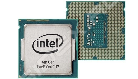 The 300Ω low side also works well. In this day and age getting large drive current from the GPIO on an MCS-48 (and MCS-51) is simply a case of slapping a MOSFET of the desired polarity straight onto the pin (you could add a gate resistor to reduce ringing, but not likely needed).
Not something that would have been done back in the day (transistors and carefully calculated bias resistors would have been used) but is exactly what I’ve done in my design. As is stated repeatedly in the databook, these pins are able to drive the inputs of other TTL logic no problems, something also found on my design.
ROM Variations
Unlike the TMS1000 which was masked-ROM only, the MCS-48 came in a cornucopia of different ROM options and sizes.
I have often seen it stated that the 8048/8049 variants were “OTP” (one-time programmable). This is (sort-of) true. They were actually mask ROM programmed.
The code for masked ROMs for these devices was supplied to Intel by customers on punched-cards. The databook explains how these are to be formatted.
Punched-card format for ordering masked ROMs from Intel.
Mask ROM Versions:
- 8048: 1K(byte) ROM, 64 bytes RAM.
- 8049: 2K(byte) ROM, 128 bytes RAM.
- 8050: 4K(byte) ROM, 256 bytes RAM.
UV/OTP EPROM Versions:
- 8748: 1K(byte) EPROM, 64 bytes RAM.
- 8749: 2K(byte) EPROM, 128 bytes RAM.
ROMless Versions:
- 8035: Up to 4K(byte) ROM, 64 bytes RAM.
- 8039: Up to 4K(byte) ROM, 128 bytes RAM.
- 8040: Up to 4K(byte) ROM, 256 bytes RAM (Very uncommon).
I built a small PCB with an EPROM socket for running ROMless devices. A de-bounced reset circuit is included, as well as a header with the latched lower address lines for the external bus. This was mainly built to help me with the debugging on the software during development (I did use a logic analyser for some of it). Gerbers for it are included at the end of this page.
The UPI-41
A typical 8042 found in a Kaypro 286 with some variety of keyboard controller mask ROM.
It would’t be fair to have gone to all this trouble only to leave out this notable variant of the MCS-48. The first Universal Peripheral Interface was the 8041 followed by the 8042 (along with 8741 and 8742 EPROM versions).
The UPI differs from a regular variety MCS-48 in that its bus interface is a slave, whereas the 8×48/8×49’s is a master. Its instruction set is also slightly different to a regular MCS-48. They are intended for creating intelligent peripherals attached to the bus of another kind of microprocessor.
The most famous application of the UPI was in the IBM AT, using an 8042 as its keyboard controller (it did some other quirky stuff too), originally programmed with the IBM “1503033” ROM image. In subsequent years its code was extended to support PS/2 mice. The 8042 was only retired from PC architecture relatively recently. Modern PCs still emulate it to allow legacy operating systems to make use of USB keyboards.
The UPI 8042 is the only member of the MCS-48 family documented to implement code security (preventing code reads of programmed parts). Because of this, code for a 8042 based keyboard controllers is difficult to come by.
I thought it would be interesting to do an experiment to see if I could make a UPI-41 do something other than look pretty in a piece of anti-static foam. Because my temperature sensor doesn’t need the bus for its main mode of operation, it will run on an 8741 or 8742 just fine with main software image. But that’s boring.
So I went to the trouble of writing another small program for it which accepts data from a ‘master’ temperature sensor.
The ROM PCB wouldn’t be required if an 8749 were used – needed because the master image requires more data and program memory than the 8748 provides. I didn’t have a working one at the time of shooting the above image.
In the above demonstration the master board, fitted with an 8039 in this particular case, has four DS18B20 temperature sensors attached to it, and writes readings from sensors 3 and 4 the second board, which is simply a peripheral on the master board’s bus, with a couple of extra banks of displays on it.
Okay, so not particularly useful but does demonstrate the concept. The code for this is linked to at the end of this page. The UPI concept is repeated on modern microcontrollers, for example, on PICs it is implemented as the PSP (Parallel Slave Port).
Resources
Below I have provided everything needed to build the boards I’ve shown on this article.
Schematics
- Main PCB
- ROM PCB
- Master to slave wiring diagram
Gerbers
- Main PCB (77.47mm x 99.06mm)
- ROM PCB (77.47mm x 62.23mm)
BOM listing
- Main PCB (xlsx)
- Main PCB (CSV)
Software
- Standard 2 Sensor board listing (8035, 8039, 8×48 or 8×49)
- UPI Master listing (Requires 8039 or 8×49)
- UPI Slave listing (8741 or 8742)
Programming a microwave or a 40-year-old controller / Sudo Null IT News and there, somewhere else, LN1 dangles to the side. I immediately liked a good rare 2Kb RF5 ROM in a socket in gold.
 I think I’ll take it off, and the rest is boldly scrapped, because the whole board is varnished to the very best.. And then it became interesting, but what is it all about? nine0005
It turned out that this is a control board from a Soviet microwave oven of the Elektronika 23 type (aka BUVI-2 aka Fairy aka Dnepryanka). Even a diagram of the device was quickly found on the Internet: http://www.elremont.ru/small_rbt/bt_rem32.php Now, when it became clear what it is, one hand confidently reached for the trash can, and the other accidentally typed “PBE035” into Google and … And I became interested and carefully looked at the board. Since there is a controller, it means that you can write programs for it. Even right on the board there is some kind of screen (4 digits) where you can display all sorts of obscene curses (BABA, SISI, well, you understand). There is also a piezo element here, which means you can squeak. Everything else can be connected to a 4×4 keyboard. This is just some kind of devboard, I was delighted! nine0003
As already mentioned, the PBE035 controller is installed on the board. In Russia, it is better known by the name KR1816BE35, but in general, it is the great and terrible Intel 8035 of the MSC-48 series. The first copies began to be produced in 1976, that is, about 40 years ago. The controller does not have its own memory for programs, so it communicates via an external bus with ROM, from where it reads instructions for execution. But there are 64 bytes of RAM, of which approximately 32 bytes can be used as you like, and the rest are for registers and the stack. There is a timer, there is an interrupt from the timer, there is an external interrupt, there is a priority system. In short, a normal old-school controller, not like fat PICs. What the Bolsheviks have been waiting for so long. I immediately wanted to code something for him. nine0003
But first we had to solve one difficulty, namely, to connect the board. As you can see from the diagram, just + 5V is required to power the digital part, but 2.5V and 30V AC voltage are needed to power the indicator.
By the way, about the indicator — it’s a lamp! Yes, a warm tube radio tube, and not some pop LEDs. And like a lamp, it has a cathode an anode and a grid. This type of indicator is called a fluorescent-vacuum indicator. After thinking a little about the circuit, I saw that 30V changes go to the diode bridge, which means they straighten up. And even 2.5V also go to the diodes and after them to the grid, which means they also straighten up. So, you can try to connect the board to a constant voltage. Instead of 30V, I applied 12V, instead of 2.5V, I applied 3.3V from a standard ATX format power supply. To do this, soldered wiring to the board. It turned out like this:
But when I turned on the board, I was disappointed at first. Some segments on the display did not light up. At first I thought that 12 volts was not enough, but then, after carefully examining the board, I found a leak in two places next to the indicator. Called, lost. The board started up, numbers appeared on the screen to set the time and select the program mode. So, I wanted to throw it away, but in the end I fixed it. It’s time to fry.
I used the free cross-platform assembler Asm48. It’s cool that there is a version for MacOS, apparently the authors are not deprived of a sense of humor, at least I appreciated it. Well, then we download the assembler, everything is simple there: ASM48
jmp main
nop
nop
nop
nop
nop
nop
main:
mov r6,#0 ; in register r6 - 0 or 80h
forever:
mov a,r6 ; forward from register to ALU
xrl a,#080h ; a = axor 80h
outl p1,a ; output to port 1
mov r6,a ; store the value in r6
call onesec ; second delay
jmp forever ; endless cycle
;---PROCEDURES
;;;;;;;;
delay100:
mov r1,#84
loopex: mov r2,#236
loopin: djnz r2,loopin
djnz r1,loopex
mov r3,#4
loopad: djnz r3,loopad
ret
;;;;;;;;
onesec:
mov r4,#10
loop_d: call delay100
djnz r4,loop_d
ret
nine0022 After compiling the program and flashing it on the programmer in ROM 2716, I start the board and hear periodic clicks with an interval of about a second. Working! Now we had to deal with the screen. The diagram shows that the "mask" of the ABCDEFG symbol is connected to port 1. Moreover, the signal is inverted, that is, when 1 - the stick is off, when 0 - it is on. In order to set the mask of the letter "H" look at the picture:
We begin to bypass the letter from G to A, since here the bits are reversed: G is shaded, which means 1; F is shaded, so 1; E is shaded, so 1; D is not shaded, so 0 and so on. The result is: 1110110b. We remember that the signals are inverted, so we need to invert the mask itself: not 1110110b = 0001001b. Or 9h. By sending this number to port 1 we set the mask for the letter. More difficult with the choice of character. Here dynamic indication is applied. In short, the essence boils down to the fact that we constantly have to set the mask, light the first character, set the mask, light the second character, and so on. The second port is responsible for resolving the glow of the symbol, which, with the help of the m5l8243p chip, is expanded to 4-4-bit ports. To access such ports, use the MOVD command, and the ports themselves are numbered P4, P5, P6, P7. P4, as conceived by the authors, is responsible for scanning the keyboard, but P5 just sets one of the four characters for display. nine0005
At first I tried to make a dynamic indication in the main program loop, but then I used a timer for this. And in the main program loop, the indicator buffer changes, displaying the inscriptions “HELO” and “2014” at intervals of 1 second
Program source code
;DATA
.equ disp_buf, 030h ; 4 bytes buffer
;;; reset vector
0
dis i ; disable interrupts
jmp main
;;; external interrupt vector--trap
.org 3
jmp$; nop
;;; timer interrupt vector
.org7
sel rb1
mov a,#0d5h
mov t,a
mov a,#00FH
orld p5,a
mov a,disp_buf-1
add a,r5
mov r0,a
mov a,@r0
outl p1,a
mov a,r4
movd p5,a
rl a
mov r4,a
djnz r5,exit_tmr
mov r4,#0feh
mov r5,4
exit_tmr:
sel rb0
mov a,#0d8h
mov t,a
; strt t
retr
;MAIN
main:
;initialize
dis tcnti ; turn off counter
mov r1,#0
mov r5,#0
call copy_buf
sel rb1 ; time variables
mov r4,#0feh ; 1110h - CT position
mov r5,4 ; R5 = buf offset
sel rb0
mov a,#0e5h
mov t,a
strt t
en tcnti
mov a,#0ffh
movd p6,a
main_loop:
call onesec
mov a,r5
xrl a,#4
mov r5,a
mov r1,a
call copy_buf
jmp main_loop
msg_table:
. db #0c0h
.db #0c7h ;L
.db #086h ;E
.db#089h ;H
.db #099h ;4
.db #0f9h ;1
.db #0c0h ;0
.db #0a4h ;2
;;;;;;;;
delay100:
mov r6,#84
loopex: mov r2,#236
loopin: djnz r2,loopin
djnz r6,loopex
mov r6,#4
loopad: djnz r6,loopad
ret
;;;;;;;;
onesec:
mov r3,#10
loop_d: call delay100
djnz r3,loop_d
ret
;;;;;;;;
;copy from msg_table to display buffer 4 bytes
; R1 = msg_table offset
;;;;;;;;
copy_buf:
mov r0,disp_buf
mov r2.4
copy_lp:
mov a,r1
add a,#msg_table
movp a,@a
mov@r0,a
inc r0
inc r1
djnz r2,copy_lp
ret
db #0c0h
.db #0c7h ;L
.db #086h ;E
.db#089h ;H
.db #099h ;4
.db #0f9h ;1
.db #0c0h ;0
.db #0a4h ;2
;;;;;;;;
delay100:
mov r6,#84
loopex: mov r2,#236
loopin: djnz r2,loopin
djnz r6,loopex
mov r6,#4
loopad: djnz r6,loopad
ret
;;;;;;;;
onesec:
mov r3,#10
loop_d: call delay100
djnz r3,loop_d
ret
;;;;;;;;
;copy from msg_table to display buffer 4 bytes
; R1 = msg_table offset
;;;;;;;;
copy_buf:
mov r0,disp_buf
mov r2.4
copy_lp:
mov a,r1
add a,#msg_table
movp a,@a
mov@r0,a
inc r0
inc r1
djnz r2,copy_lp
ret
A short video demonstration of the device:
An inquisitive habrauser probably noticed a bug at the end of the video, when instead of HELO, not quite what was needed was highlighted. I noticed it too, yes. And all because when in the main program there is a transfer to the display buffer, I forgot to stop the timer. Before call copy_buf, you need to do DIS TCNTI and after EN TCNTI. So that!
Now it only remains to play on the device “a Christmas tree was born in the forest” and I will consider the mission successfully completed. All the best! nine0003
Literature:
1) MCS-48 AND UPI-41 ASSEMBLER LANGUAGE MANUAL 1976
2) Volume 2 of Shakhnov's Handbook (Microprocessors and microprocessor integrated circuits)
3) Stashin V.V. etc. - Designing digital devices on single-chip microcontrollers
4) Sign-synthesizing indicators: Handbook / Ed. V. P. Balashova
5) Bystrov Yu.A. One Hundred LED Circuits
Memory for Nutanix - NX-8000 Series NX-8035-G6
Memory for Nutanix - NX-8000 Series NX-8035-G6 - Kingston Technology
Search Kingston.com
To get started, click accept below to open your cookie control panel. Then click the Personalize button to enable the chat feature and then Save.
Your web browser version is out of date. Please update your browser to improve your experience on this website. https://browser-update.org/update-browser.html
nine0061
Filter
Filters
Applied
Sort by
Title - A to Z
-
Serial number: KSM26RD4/32HDI
- Serial number: KSM26RD4/32HDI
- DDR4 2666MT/s ECC Registered DIMM CL19 2RX4 1.
 2V 288-pin 8Gbit Hynix D IDT
 - Performance data in PDF
- PCN
DDR4 2666MT/s ECC Registered DIMM CL19 2RX4 1.2V 288-pin 8Gbit Hynix D IDT
- Performance data in PDF
- PCN
Where to buy
-
Serial number: KSM26RD4/32MRR
- Serial number: KSM26RD4/32MRR
- DDR4 2666MT/s ECC Registered DIMM CL19 2RX4 1.2V 288-pin 8Gbit Micron R Rambus
- Performance data in PDF
- PCN
DDR4 2666MT/s ECC Registered DIMM CL19 2RX4 1.2V 288-pin 8Gbit Micron R Rambus
-
Performance data in PDF
nine0063 - PCN
Where to buy
-
Serial number: KSM26RS4/32HCR
- Serial number: KSM26RS4/32HCR
- DDR4 2666MT/s ECC Registered DIMM CL19 1RX4 1.
 2V 288-pin 16Gbit Hynix C Rambus
 - Performance data in PDF
- PCN
DDR4 2666MT/s ECC Registered DIMM CL19 1RX4 1.2V 288-pin 16Gbit Hynix C Rambus
- Performance data in PDF
- PCN
nine0066
Where to buy
-
Serial number: KSM26RS4/32MFR
- Serial number: KSM26RS4/32MFR
- DDR4 2666MT/s ECC Registered DIMM CL19 1RX4 1.2V 288-pin 16Gbit Micron F Rambus
- Performance data in PDF
- PCN
DDR4 2666MT/s ECC Registered DIMM CL19 1RX4 1.2V 288-pin 16Gbit Micron F Rambus
- Performance data in PDF
- PCN
Where to buy
nine0003
No products were found matching your selection
Filter
Filters
Applied
Sort by
Default
-
Serial number: SEDC450R/1920G
Capacity Selections
480 GB
960 GB
1920 GB
3840 GB
7680 GB
- Enterprise-grade SSD for data centers
-
Optimized for read-heavy applications.
nine0063 - SATA Rev3.0
- Up to 560MB/s read, 530MB/s write
- Serial number: SEDC450R/1920G
- PCN
- Learn more
Where to buy
-
Serial number: SEDC500M/1920G
Capacity Selections
480GB
960GB
1920GB
3840GB
- Optimized for mixed tasks
-
Life at 1.
 3DWPD
3DWPD
nine0063 - Consistent input/output operations per second (IOPS), reliable QoS and low latency.
- Configurable increase in the spare area of the drive.
- Integrated Power Loss Protection (PLP)
- Serial number: SEDC500M/1920G
- PCN
- Learn more
Where to buy
-
Serial number: SEDC450R/3840G
Capacity Selections
480 GB
960GB
1920GB
3840GB
7680GB
- Enterprise-grade SSD for data centers
- Optimized for read-heavy applications.
- SATA Rev3.0
- Up to 560MB/s read, 525MB/s write
- Serial number: SEDC450R/3840G
- PCN
- Learn more
Where to buy
-
Serial number: SEDC500M/3840G
Capacity Selections
480GB
960GB
1920GB
3840GB
- Optimized for mixed tasks
- Life at 1.3DWPD
- Consistent input/output operations per second (IOPS), reliable QoS and low latency.
- Configurable increase in the spare area of the drive.
-
Integrated Power Loss Protection (PLP)
nine0063 - Serial number: SEDC500M/3840G
- PCN
- Learn more
Where to buy
-
Serial number: SEDC500R/3840G
Capacity Selections
480GB
960GB
3840GB
7680GB
-
Optimized for read-heavy tasks.
- Life at 0.5DWPD
-
Stable input/output operations per second (IOPS), reliable quality of service (QoS) and low latency.
nine0063 - Configurable increase in the spare area of the drive.
- Integrated Power Loss Protection (PLP)
- Serial number: SEDC500R/3840G
- PCN
- Learn more
Where to buy
-
Optimized for read-heavy tasks.
-
Serial number: SEDC450R/480G
Capacity Selections
480 GB
960 GB
1920 GB
3840 GB
7680 GB
-
Enterprise-grade SSD for data centers
nine0063 - Optimized for read-heavy applications.
- SATA Rev3.0
- Up to 560MB/s read, 510MB/s write
- Serial number: SEDC450R/480G
- PCN
- Learn more
Where to buy
-
Enterprise-grade SSD for data centers
-
Serial number: SEDC500M/480G
Capacity Selections
480GB
960GB
1920GB
3840GB
-
Optimized for mixed tasks
nine0063 - Life at 1.3DWPD
- Consistent input/output operations per second (IOPS), reliable QoS and low latency.
- Configurable increase in the spare area of the drive.
- Integrated Power Loss Protection (PLP)
- Serial number: SEDC500M/480G
- PCN
- Learn more
Where to buy
-
Optimized for mixed tasks
-
Serial number: SEDC500R/480G
Capacity Selections
nine0004 480GB960GB
3840GB
7680GB
-
Optimized for read-heavy tasks.

- Life at 0.5DWPD
- Stable input/output operations per second (IOPS), reliable quality of service (QoS) and low latency.
- Configurable increase in the spare area of the drive.
- Integrated Power Loss Protection (PLP)
-
Serial number: SEDC500R/480G
nine0063 - PCN
- Learn more
Where to buy
-
Optimized for read-heavy tasks.
-
Serial number: SEDC450R/7680G
Capacity Selections
480 GB
960 GB
1920 GB
3840 GB
7680 GB
- Enterprise-grade SSD for data centers
- Optimized for read-heavy applications.
- SATA Rev3.0
-
Up to 560MB/s read, 504MB/s write
nine0063 - Serial number: SEDC450R/7680G
- PCN
- Learn more
Where to buy
-
Serial number: SEDC500R/7680G
Capacity Selections
480GB
960GB
3840GB
7680GB
- Optimized for read-heavy tasks.
- Life at 0.6DWPD
-
Stable input/output operations per second (IOPS), reliable quality of service (QoS) and low latency.
nine0063 - Configurable increase in the spare area of the drive.
- Integrated Power Loss Protection (PLP)
- Serial number: SEDC500R/7680G
- PCN
- Learn more
Where to buy
-
Serial number: SEDC450R/960G
Capacity Selections
480 GB
960 GB
1920 GB
3840 GB
7680 GB
-
Enterprise-grade SSD for data centers
nine0063 -
Optimized for read-heavy applications.

- SATA Rev3.0
- Up to 560MB/s read, 530MB/s write
- Serial number: SEDC450R/960G
- PCN
- Learn more
Where to buy
-
Enterprise-grade SSD for data centers
-
Serial number: SEDC500M/960G
Capacity Selections
480GB
960GB
1920GB
3840GB
-
Optimized for mixed tasks
nine0063 - Life at 1.3DWPD
- Consistent input/output operations per second (IOPS), reliable QoS and low latency.
- Configurable increase in the spare area of the drive.
- Integrated Power Loss Protection (PLP)
- Serial number: SEDC500M/960G
- PCN
- Learn more
Where to buy
-
Optimized for mixed tasks