Intel Core i7 4960X (Ivy Bridge E) Review
by Anand Lal Shimpion September 3, 2013 4:10 AM EST
- Posted in
- CPUs
- Intel
- Ivy Bridge
- Ivy Bridge-E
120 Comments
|
120 Comments
Introduction & The DetailsMemory & General Purpose PerformanceVideo Transcoding & 3D Rendering PerformanceVisual Studio, Photoshop, File Compression & Excel Math PerfGaming PerformanceOverclocking & Power ConsumptionFinal Words
Twenty two months ago Intel launched its LGA-2011 platform and Sandy Bridge E aimed at the high-end desktop enthusiast. The platform brought more cores, more PCIe lanes and more memory bandwidth to those users who needed more than what had become of Intel’s performance desktop offerings. It was an acknowledgement of a high end market that seems to have lost importance over the past few years. On the surface, Sandy Bridge E was a very good gesture on Intel’s part. Unfortunately, the fact that it’s been nearly two years since we first met LGA-2011 without a single architecture update, despite seeing the arrival of both Ivy Bridge and Haswell, doesn’t send a great message to the users willing to part with hard earned money to buy into the platform.
Today we see that long awaited update. LGA-2011 remains unchanged, but the processor you plug into the socket moves to 22nm. This is Ivy Bridge Extreme.
Ivy Bridge E: 1.86B Transistors, Up to 6 Cores & 15MB L3
There’s a welcoming amount of simplicity in the Extreme Edition lineup. There are only three parts to worry about:
With the exception of the quad-core 4820K, IVB-E launch pricing is identical to what we saw with Sandy Bridge E almost two years ago. The 4820K is slightly cheaper than the highest end Haswell part, but it’s still $25 more expensive than its SNB-E counterpart was at launch.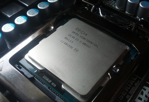 The difference? The 4820 is a K-SKU, meaning it’s fully unlocked, and thus comes with a small price premium.
All of the IVB-E parts ship fully unlocked, and are generally capable of reaching the same turbo frequencies as their predecessors. The Core i7-4960X and the i7-3970X before it, are the only Intel CPUs officially rated for frequencies of up to 4GHz (although we’ve long been able to surpass that via overclocking). Just as before, none of these parts ship with any sort of cooling (because profit), you’ll need to buy a heatsink/fan or closed loop water cooler separately. Intel does offer a new cooler for IVB-E, the TS13X:
While Sandy Bridge E was an 8-core die with two cores disabled, Ivy Bridge E shows up in a native 6-core version. There’s no die harvesting going on here, all of the transistors on the chip are fully functional. The result is a significant reduction in die area, from the insanity that was SNB-E’s 435mm2 down to an almost desktop-like 257mm2.
| CPU Specification Comparison | |||||||||
| CPU | Manufacturing Process | Cores | GPU | Transistor Count (Schematic) | Die Size | ||||
| Haswell GT3 4C | 22nm | 4 | GT3 | ? | 264mm2 (est) | ||||
| Haswell GT2 4C | 22nm | 4 | GT2 |
1. 4B 4B |
177mm2 | ||||
| Haswell ULT GT3 2C | 22nm | 2 | GT3 | 1.3B | 181mm2 | ||||
| Intel Ivy Bridge E 6C | 22nm | 6 | N/A | 1.86B | 257mm2 | ||||
| Intel Ivy Bridge 4C | 22nm | 4 | GT2 | 1.2B | 160mm2 | ||||
| Intel Sandy Bridge E 6C | 32nm | 6 | N/A |
2. 27B 27B |
435mm2 | ||||
| Intel Sandy Bridge 4C | 32nm | 4 | GT2 | 995M | 216mm2 | ||||
| Intel Lynnfield 4C | 45nm | 4 | N/A | 774M | 296mm2 | ||||
| AMD Trinity 4C | 32nm | 4 | 7660D | 1.303B | 246mm2 | ||||
| AMD Vishera 8C | 32nm | 8 | N/A |
1. 2B 2B |
315mm2 | ||||
Cache sizes remain unchanged. The highest end SKU features a full 15MB L3 cache, while the mid-range SKU comes with 12MB and the entry-level quad-core part only has 10MB. Intel adds official support for DDR3-1866 (1 DIMM per channel) with IVB-E, up from DDR3-1600 in SNB-E and Haswell.
TDPs all top out at 130W, bringing back memories of the high-end desktop SKUs of yesterday. Obviously these days much of what we consider to be high-end exists below 100W.
Of course processor graphics is a no-show on IVB-E. As IVB-E retains the same socket as SNB-E, there are physically no pins set aside for things like video output. Surprisingly enough, early rumors indicate Haswell E will also ship without an integrated GPU.
The Extreme Cadence & Validated PCIe 3.0
Understanding why we’re talking about Ivy Bridge E now instead of Haswell E is pretty simple. The Extreme desktop parts come from the Xeon family. Sandy Bridge E was nothing more than a 6-core Sandy Bridge EP variant (Xeon E5), and Ivy Bridge E is the same. In the Xeon space, the big server customers require that Intel keep each socket around for at least two generations to increase the longevity of their platform investment. As a result we got two generations of Xeon CPUs (SNB-E/EP, and IVB-E/EP) that leverage LGA-2011. Because of when SNB-E was introduced, the LGA-2011 family ends up out of phase with the desktop/notebook architectures by around a year. So we get IVB-E in 2013 while desktop/notebook customers get Haswell. Next year when the PC clients move to 14nm Broadwell, the server (and extreme desktop) customers will get 22nm Haswell-E.
The only immediate solution to this problem would be for the server parts to skip a generation — either skip IVB-E and go to Haswell-E (not feasible as that would violate the 2 generations rule above), or skip Haswell-E and go directly to Broadwell-E next year. Intel tends to want to get the most use out of each one of its architectures, so I don’t see a burning desire to skip an architecture.
Server customers are more obsessed with core counts than modest increases in IPC, so I don’t see a lot of complaining there. On the desktop however, Ivy Bridge E poses a more interesting set of tradeoffs.
The big advantages that IVB-E brings to the table are a ridiculous number of PCIe lanes, a quad-channel memory interface and 2 more cores in its highest end configuration.
While the standard desktop Sandy Bridge, Ivy Bridge and Haswell parts all feature 16 PCIe lanes from the CPU’s native PCIe controller, the Extreme parts (SNB-E/IVB-E) have more than twice that.
There are 40 total PCIe 3.0 lanes that branch off of Ivy Bridge E. Since IVB-E and SNB-E are socket compatible, that’s the same number of lanes we got last time. The difference this time around is IVB-E’s PCIe controller has been fully validated with PCIe 3.0 devices. While Sandy Bridge E technically supported PCIe 3.0 the controller was finalized prior to PCIe 3.0 devices being on the market and thus wasn’t validated with any of them.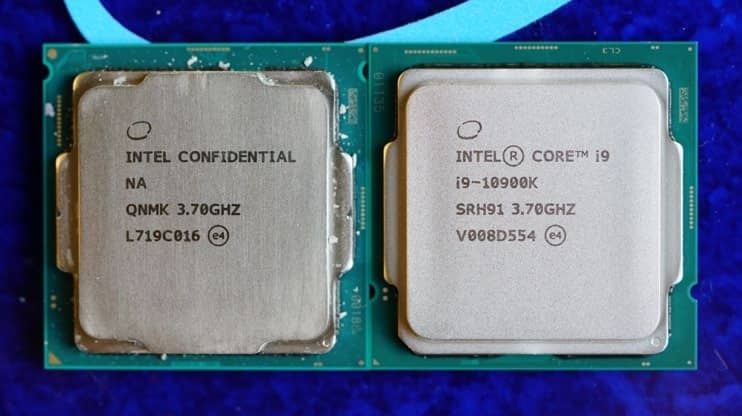 The most famous case being NVIDIA’s Kepler cards which by default run in PCIe 2.0 mode on SNB-E systems. Forcing PCIe 3.0 mode on SNB-E worked in many cases, while in others you’d see instability.
NVIDIA tells us that it plans to enable PCIe 3.0 on all IVB-E systems. Current drivers (including the 326.80 beta driver) treat IVB-E like SNB-E and force all Kepler cards to PCIe 2.0 mode, but NVIDIA has a new driver going through QA right now that will default to PCIe 3.0 when it detects IVB-E. SNB-E systems will continue to run in PCIe 2.0 mode.
Gallery: Intel Core i7 4960X (Ivy Bridge E) Review
Intel’s X79: Here for One More Round
Unlike its mainstream counterpart, Ivy Bridge E does not come with a new chipset. That’s right, not only is IVB-E socket compatible with SNB-E, it ships with the very same chipset: X79.
As a refresher Intel’s X79 chipset has no native USB 3.0 support and only features two native 6Gbps SATA ports. Motherboard makers have worked around X79’s limitations for years now by adding a plethora of 3rd party controllers. I personally prefer Intel’s native solutions to those we find from 3rd parties, but with X79 you’ve got no choice.
The good news is that almost all existing X79 motherboards will see BIOS/EFI updates enabling Ivy Bridge E support. The keyword there is almost.
When it exited the desktop motherboard market, Intel only promised to release new Haswell motherboards and to support them through the end of their warranty period. Intel never promised to release updated X79 motherboards for Ivy Bridge E, nor did it promise to update its existing X79 boards to support the new chips. In a very disappointing move, Intel confirmed to me that none of its own X79 boards will support Ivy Bridge E. I confirmed this myself by trying to boot a Core i7-4960X on my Intel DX79SI — the system wouldn’t POST. While most existing X79 motherboards will receive BIOS updates enabling IVB-E support, anyone who bought an Intel branded X79 motherboard is out of luck. Given that LGA-2011 owners are by definition some of the most profitable/influential/dedicated customers Intel has, I don’t think I need to point out how damaging this is to customer relations. If it’s any consolation, IVB-E doesn’t actually offer much of a performance boost over SNB-E — so if you’re stuck with an Intel X79 motherboard without IVB-E support, you’re not missing out on too much.
The Testbed: ASUS’ New X79 Deluxe
As all of my previous X79 boards were made by Intel, I actually had no LGA-2011 motherboards that would work with IVB-E on hand. ASUS sent over the latest revision of its X79 Deluxe board with official IVB-E support:
The board worked relatively well but it seems like there’s still some work that needs to be done on the BIOS side. When loaded with 32GB of RAM I saw infrequent instability at stock voltages. It’s my understanding that Intel didn’t provide final BIOS code to the motherboard makers until a couple of weeks ago, so don’t be too surprised if there are some early teething pains. For what it’s worth, that this makes Ivy Bridge E the second high-end desktop launch in a row that hasn’t gone according to Intel’s previously high standards.
Corsair supplied the AX1200i PSU and 4 x 8GB DDR3-1866 Vengeance Pro memory for the testbed.
For more comparisons be sure to check out our performance database: Bench.
| Testbed Configurations | ||||
| Motherboard(s) |
ASUS X79 Deluxe |
|||
| Memory |
Corsair Vengeance DDR3-1866 9-10-9-27 |
|||
| SSD |
Corsair Neutron GTX 240GB |
|||
| Video Card |
NVIDIA GeForce GTX Titan x 2 (only 1 used for power tests) |
|||
| PSU |
Corsair AX1200i |
|||
| OS |
Windows 8 64-bit |
|||
Memory & General Purpose Performance
Introduction & The DetailsMemory & General Purpose PerformanceVideo Transcoding & 3D Rendering PerformanceVisual Studio, Photoshop, File Compression & Excel Math PerfGaming PerformanceOverclocking & Power ConsumptionFinal Words
Tweet
PRINT THIS ARTICLE
Intel Core i7-4960X Review: Ivy Bridge-E, Benchmarked
Update (9/3/2013): The following story was originally published on July 16th, 2013. After receiving a second Core i7-4960X sample, we validated the correctness of our numbers and updated the piece with official information from Intel.
Recently, Gartner published numbers showing that shipments of PCs dropped a staggering 11 percent in the second quarter of this year, primarily attributed to tablets replacing entry-level machines. Wall Street, at least, is all doom and gloom about the PC’s future prospects.
But the boutique builders I talk to say that interest in super-fast gaming systems is at an all-time high thanks to the efficiency of certain processor and graphics architectures. So, while now might be a bad time to get stoked about mainstream hardware, performance-oriented power users have some pretty quick components to choose from.
None of this is news to enthusiasts. In fact, two and a half years ago, Intel’s Sandy Bridge architecture was serving up compelling performance under 100 W. Those were exciting times. The Ivy Bridge architecture that followed nudged our benchmark results forward a bit, but dropped power to less than 77 W.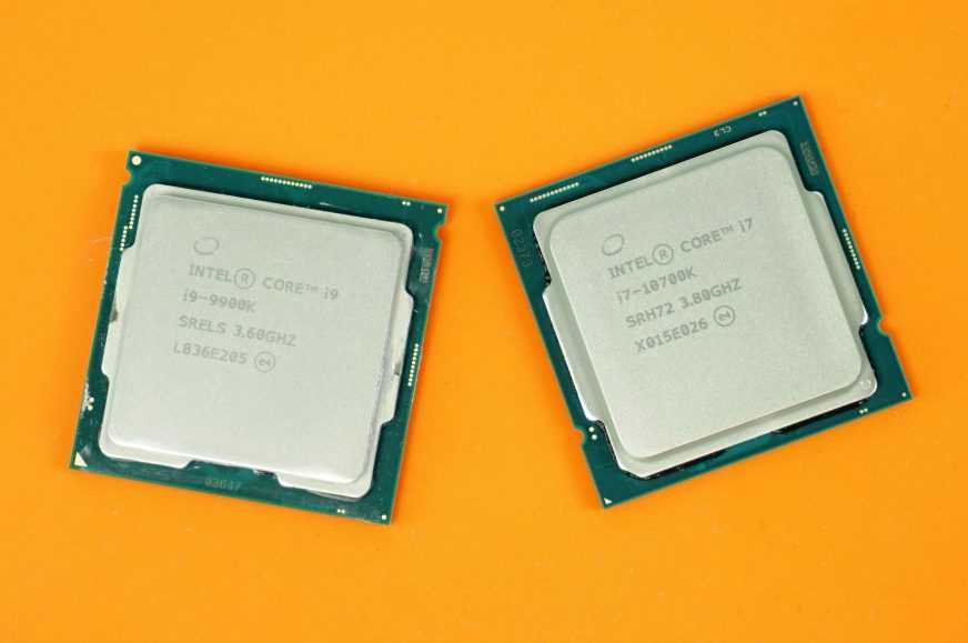 That was pretty cool, too. More recently, Haswell added another few percentage points to the performance picture, but bumped maximum consumption back up to 84 W.
Now, if you’re upgrading an old Core 2- or Phenom II-based machine with a $5000 boutique build, the latest parts are going to feel wicked-fast, no matter how incremental the previous two or three generations look on paper. The difference is simply less perceptible to those of us working with these components day in and out.
The point is that, for a do-it-yourselfer like me, Sandy Bridge was exciting, Ivy Bridge a little less so, and Haswell…well, I called that one The Core i7-4770K Review: Haswell Is Faster; Desktop Enthusiasts Yawn.
We all know where Intel’s collective mind is: the mobile space where those Gartner guys are telling us the low-end PCs continue getting slaughtered. In that context, spending $350 on a -4770K and another $250 on an LGA 1150-capable motherboard just to keep up with the Kardashians doesn’t sound so hot.
If, a year and a half ago, you snagged a Core i7-3930K (which won a very rare Best Of award from us in Intel Core i7-3930K And Core i7-3820: Sandy Bridge-E, Cheaper), you’d still be sitting pretty, potentially overclocked to 4.5 or 4.6 GHz, and outclassing the -4770K in a great many threaded applications. You’d also be using the same X79-based platform. And, with the revelation that Intel’s upcoming Ivy Bridge-E architecture will drop into an LGA 2011 interface, you’re also going to face your first opportunity in two years to buy something faster.
Meet Ivy Bridge-E, The Upgrade Path For X79 Express
From most angles, the Ivy Bridge-E-based parts look a lot like Sandy Bridge-E, except for the adoption of Intel’s Ivy Bridge architecture. That means a handful of IPC-oriented improvements in the core, cache, and memory controller, similar to what we described in Intel Core i7-3770K Review: A Small Step Up For Ivy Bridge. Of course, gone is the emphasis on graphics. That means Ivy Bridge-E is really about the updated core, a memory controller rated for 1866 MT/s (instead of 1600), official PCI Express 3.0 compliance (remember, Sandy Bridge-E only claimed 8 GT/s signaling support), and 22 nm manufacturing. Ivy Bridge-E-based CPUs are also unlocked up to 63x multipliers (versus SNB-E’s 57x), you should be able to hit memory data rates beyond 2400 MT/s, Ivy Bridge-E supports XMP 1.3 (compared to SNB-E’s XMP 1.2), and you’ll have access to real-time ratio, voltage, and power limit settings.
Intel’s Ivy Bridge-E die; six CPU cores are clearly visible, along with shared L3 cache and the memory controller up top
You still get 40 lanes of PCI Express connectivity, divisible into as many ports as you need for four-way CrossFire and SLI. You’re still dealing with a quad-channel memory controller, though the higher data rate increases peak bandwidth to 59.7 GB/s from 51.2 GB/s. And you’re dropping Ivy Bridge-E into the aging X79 Express platform.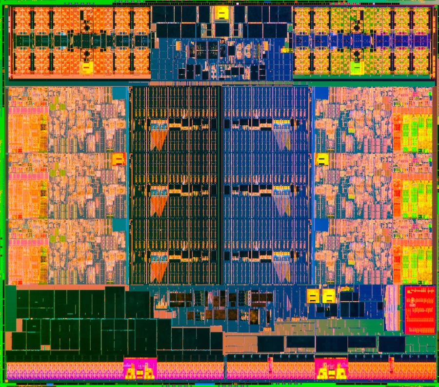 The good news is that your old motherboard still works; you don’t have to buy a new one. Unfortunately, the chipset only offers two SATA 6Gb/s ports, it doesn’t feature native USB 3.0, and you don’t get to enjoy new capabilities like SATA Express, which is expected to surface alongside Haswell-based 9-series chipsets early in 2014.
Swipe to scroll horizontally
| Header Cell — Column 0 | Core i7-4960X | Core i7-4930K | Core i7-4820K | Core i7-3970X |
|---|---|---|---|---|
| Code Name | Ivy Bridge-E | Ivy Bridge-E | Ivy Bridge-E | Sandy Bridge-E |
| Base Clock Rate | 3.6 GHz | 3.4 GHz | 3.7 GHz | 3.5 GHz |
| Maximum Turbo Boost | 4 GHz | 3. 9 GHz 9 GHz |
3.9 GHz | 4 GHz |
| PCI Express Link Speed | 8 GT/s | 8 GT/s | 8 GT/s | 8 GT/s |
| TDP | 130 W | 130 W | 130 W | 150 W |
| Processor Cores | 6 | 6 | 4 | 6 |
| Shared L3 Cache | 15 MB | 12 MB | 10 MB | 15 MB |
| Max. Memory Data Rate | DDR3-1866 | DDR3-1866 | DDR3-1866 | DDR3-1600 |
| Processor Interface | LGA 2011 | LGA 2011 | LGA 2011 | LGA 2011 |
| Price | $990 | $555 | $310 | $1020 (Street) |
Again, Core i7-4960X is a six-core part with 15 MB of shared L3 cache. No doubt that’ll disappoint the folks who were hoping a 22 nm process would make it easier for Intel to arm enthusiasts with eight or 12 cores (it actually does, as we saw in Intel’s 12-Core Xeon With 30 MB Of L3: The New Mac Pro’s CPU?). But, at the same ~$1000 price point, there’s really no reason to give you a more complex CPU when it’s already charging $1900 for an eight-core Xeon E5-2687W. And so, anyone considering a move from today’s Core i7-3970X can expect an additional 100 MHz base frequency, the same 4 GHz peak Turbo Boost clock rate, and the other incremental improvements.
The Core i7-4820K is a little more interesting. Realizing that there was almost no reason at all anyone would want a multiplier-locked, quad-core -3820, Intel gives its successor an unlocked ratio. It’s still a quad-core chip with 10 MB of shared L3 cache based on a previous-gen architecture in a previous-gen platform. But perhaps the additional PCI Express connectivity, memory bandwidth, and L3 cache, coupled with the ability to overclock, makes the -4820K competitive against Intel’s Haswell-based Core i7-4770K.
And then there’s the Core i7-4930K, which retains six cores, sheds a little of its shared L3 cache (dropping to 12 MB), and drops a little frequency (200 MHz base clock and 100 MHz peak Turbo Boost), but also costs close to half of what you’d pay for the flagship. That’s the model we were most excited about last generation. We reserve some of that excitement today, realizing that enthusiasts who bought a -3930K probably won’t step up to a -4930K for another $500+ dollars.
Curiously, all three Ivy Bridge-E-based parts are accompanied by 130 W thermal design power limits. Remember that the move from Sandy to Ivy Bridge yielded a more complex CPU with a significantly lower power ceiling, thanks in no small part to a shift from 32 to 22 nm manufacturing. Here, we have the same process transition. The die shrinks from Sandy Bridge-E’s 434 square millimeters down to 257. Intel even cites a lower transistor count for Ivy Bridge-E (1.86 billion versus SNB-E’s 2.27 billion).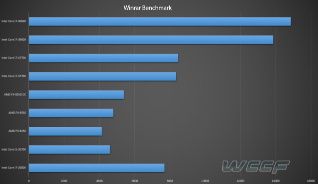 And yet, this new CPU shares the same 130 W rating as Core i7-3960X and -3930K. Keep an eye on this. Power may just become Ivy Bridge-E’s greatest strength.
- 1
Current page:
Ivy Bridge-E: Core i7-4960X Gets Tested
Next Page Test Setup And Benchmarks
Chris Angelini is an Editor Emeritus at Tom’s Hardware US. He edits hardware reviews and covers high-profile CPU and GPU launches.
Review and testing of the Intel Core i7-4960X Extreme Edition processor GECID.com. Page 1
::>Processors
>2013
> Intel Core i7-4960X Extreme Edition
09/16/2013
Page 1
Page 2
One page
This year, Intel has planned to release several new families of processors, including Intel Haswell and Intel Ivy Bridge-E. And if the first has already managed to gain a foothold in the market of computer components, then the presentation of the second took place just the other day.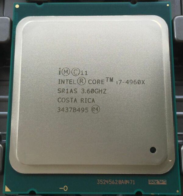 Of course, we could not ignore such an event, so we decided to devote a separate article to it. Moreover, we will get acquainted with the new generation of processors based on the «top» model — Intel Core i 7-4960 X Extreme Edition . But we’ll talk about it a little later, but now let’s take a closer look at the features of the Intel Ivy Bridge-E architecture.
Architecture Intel Ivy Bridge-E
The Intel Ivy Bridge-E family of processors, like Intel Sandy Bridge-E, belongs to high-end class solutions with high performance and rather high price. Therefore, it is not surprising that the company decided not to change the processor socket, making the Intel Ivy Bridge-E models fully compatible with the Socket LGA2011 platform already on the market. For many users, this was good news, since updating such a system is not a cheap pleasure.
In the absence of real competition in this market segment, Intel does not need to force things and make some major improvements to its «top» platform. Therefore, you will not see an increase in the number of cores or a special increase in clock speed in Intel Ivy Bridge-E. In fact, the transition to a new microarchitecture and a more subtle process technology just took place. Although it can be called «new» with great convention, since the Intel Ivy Bridge microarchitecture has been on the market for a long time in the form of processors for the Socket LGA1155 platform and is quite well studied in our test laboratory.
However, to say that the company released just a copy of the previous generation, of course, is impossible. Compared to Intel Sandy Bridge-E, there are many changes in the Intel Ivy Bridge-E microarchitecture. The main ones are the transition from 32nm to 22nm process technology, the introduction of official support for the PCI-Express 3.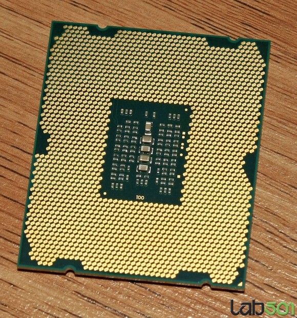 0 bus and memory with a speed of DDR3-1866 MHz (instead of DDR3-1600 MHz for Intel Sandy Bridge-E). Some improvements have also been made to the core, cache, and memory controller to increase the number of instructions executed per clock. We considered these features during the analysis of the Intel Ivy Bridge microarchitecture, so we will not dwell on them in more detail.
The die on which the Intel Ivy Bridge-E processors are made has also changed.
Photo of the Crystal of the Family processor Intel Sandy Bridge-E
Photo of the Family Crystal Intel Ivy Bridge-E
while based a crystal with eight computing cores, two of which were simply blocked, for Intel Ivy Bridge-E the company designed a specialized crystal with six computing cores. At the same time, its area was reduced (from 435 to 257 sq. mm), as well as the number of transistors used (from 2.27 to 1.86 billion). That is, from a technical point of view, the cost of Intel Ivy Bridge-E should be lower than that of their predecessors. There is no integrated video core, which is quite logical.
Intel emphasizes that the Socket LGA2011 platform is primarily intended for processing and creating multimedia content, overclocking experiments and building gaming configurations with multiple video cards. And in each of these cases, the possibility of overclocking is a rather popular option.
Therefore, some innovations have been noticed in Intel Ivy Bridge-E processors here too: support for real-time overclocking has been added (without the need to restart the computer for the settings to take effect) and the maximum supported multiplier has been increased (from 57 to 63). Also, let’s not forget that Intel Ivy Bridge-E supports bus overclocking, but, as a rule, within small limits. Metal is used as a thermal interface, not thermal paste (like Intel Ivy Bridge and Intel Haswell). This means that the heat from the new processors for the Socket LGA2011 platform can be removed without unnecessary obstacles with maximum efficiency.
If we consider the capabilities of the entire Socket LGA2011 platform as a whole, they have not changed much. For the needs of the graphics system, 40 PCI Express lanes are still allocated already in version 3.0, and the memory controller can operate in a four-channel mode. True, in the latter case, the increased data transfer rate increases the peak throughput from 51.2 GB / s to 59.7 GB / s.
The Intel X79 Express chipset also imposes its limitations, which provides only two SATA 6 Gb / s ports and does not support the USB 3.0 interface. Although users should not worry about this once again. Motherboard manufacturers easily circumvent these limitations by using additional third-party controllers on their solutions, which significantly expand the functionality of the Socket LGA2011 platform.
Lineup
At the moment, the Intel Ivy Bridge-E family is represented by only three processors, and this number is not planned to increase in the near future.
|
Model |
Intel Core i7-4960X Extreme Edition |
Intel Core i7-4930K |
Intel Core i7-4820K |
|
Frequency (base/Turbo), GHz |
3.6/4.0 |
3.4/3.9 |
3.7/3.9 |
|
Number of cores/threads |
6/12 |
6/12 |
4/8 |
|
Third level cache (L3), MB |
15 |
12 |
10 |
|
Memory controller |
4-channel DDR3-1866 MHz support |
4-channel DDR3-1866 MHz support |
4ch supporting DDR3-1866MHz |
|
Thermal package (TDP), W |
130 |
130 |
130 |
|
Wholesale price (in a lot from 1000 pieces), USD |
990 |
555 |
310 |
By the names of new products it is easy to determine which models they will replace in the computer components market. Note that for the Intel Core i7-3970X, an analogue in the Intel Ivy Bridge-E processor family is not yet expected.
As can be seen from the table, the number of cores/threads, as well as the size of the third-level cache remained the same, the clock frequency grew by 100-200 MHz, depending on the model. The thermal package of all new products fits into the value of 130 watts. We also note that the “younger” Intel Core i7-4820K model has an unlocked multiplier, while this option was disabled in the Intel Core i7-3820.
appearance and packaging
And now let’s move from theory to practice and consider in more detail the flagship model of the Intel Ivy Bridge-E family- Intel Core 7-0007 7-4960 Extreme Edition . An engineering sample of the processor came to our test lab, so there is no description of the packaging and cooling system.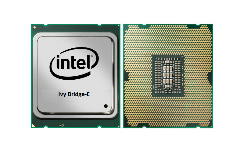
Despite the fact that the dimensions of the used crystal have decreased, externally the Intel Core i7-4960X Extreme Edition processor is absolutely no different from its predecessor from the Intel Sandy Bridge-E generation. On the heat-distributing cover the marking, clock frequency and the name of the country of the manufacturer, in this case Costa Rica, are indicated.
60X Extreme Edition and, for example, Intel Core i7-3930K there is no difference.
Specification
|
Model |
Intel Core i7-4960X Extreme Edition |
|
Marking |
QF7Z |
|
Processor socket |
Socket LGA2011 |
|
Clock frequency (nominal), MHz |
3600 |
|
Maximum clock speed with Turbo Core 3. |
4000 |
|
Multiplier |
36 |
|
Bus frequency, MHz |
100 |
|
L1 cache size, KB |
6 x 32 (instruction memory) 6 x 32 (data memory) |
|
L2 cache size, KB |
6 x 256 |
|
L3 cache size, MB |
15 |
|
Microarchitecture |
Intel Ivy Bridge |
|
Core |
Intel Ivy Bridge-E |
|
Number of cores/threads |
6/12 |
|
Instruction support |
MMX, SSE, SSE2, SSE3, SSSE3, SSE4.1, SSE4.2, EM64T, VT-x, AES, AVX |
|
Supply voltage, V |
— |
|
Power dissipation, W |
130 |
|
Critical temperature, °C |
— |
|
Process |
22 nm |
|
Technology Support |
Enhanced Halt State (C1E) Enhanced Intel Speedstep Hyper Threading Execute Disable Bit Intel Virtualization Intel Turbo Boost |
|
Built-in memory controller |
|
|
Maximum memory size, GB |
128 |
|
Memory types |
DDR3 (up to 1866 MHz) |
|
Number of memory channels |
4 |
|
Maximum throughput, GB/s |
to 59. |
 0, MHz
  7
7 The CPU-Z program confirms the information written in the table above. As can be seen from the screenshot, in normal operation (Intel Turbo Boost technology is disabled), the clock frequency of the Intel Core i7-4960X Extreme Edition is 3600 MHz, with a bus speed of 100 MHz and a multiplier of «x36». At the time of reading, the voltage on the core was 1.104 V.
If you use the dynamic boost mode or just the “automatic overclocking” function using proprietary Turbo Boost technology, the multiplier increases by four points to the value “x40”. At the same time, the processor speed increases to 4000 MHz, and the voltage to 1.248 V.
In idle mode, the multiplier decreases to the value “x12”, thereby reducing the frequency to 1200 MHz. The voltage is 0.824 V.
The cache memory of the Intel Core i7-4960X Extreme Edition is distributed similarly to the «top» processors from the Intel Sandy Bridge-E family. The cache memory of the first level L1 is 64 KB per core, of which 32 KB is for data caching and the same amount for instructions. L2 cache memory has a capacity of 256 KB per core. The cache memory of the third level L3 is shared by the entire processor, its size is 15 MB. For L1 and L2 caches, 8 associativity lines are used, while for L3 — 20.
The DDR3 memory controller operates in 4-channel mode and supports RAM up to 1866 MHz.
Testing
Intel Core i7-4960X Processor Review: Specifications, Benchmark Tests
The Core i7-4960X processor was released by Intel, release date: September 3, 2013. At the time of release, the processor cost $999. The processor is designed for desktop computers and is based on the Ivy Bridge E architecture.
Processor unlocked for overclocking. The total number of cores is 6, threads — 12. The maximum clock speed of the processor is 4.00 GHz. The maximum temperature is 66. 8°C. Technological process — 22 nm. Cache size: L1 — 384 KB, L2 — 1.5 MB, L3 — 15 MB.
Supported memory type: DDR3 1333/1600/1866. Maximum supported memory size: 64 GB.
Supported socket type: FCLGA2011. The maximum number of processors in the configuration is 1. Power consumption (TDP): 130 Watt.
Benchmarks
| PassMark Single thread mark |
|
|||||
| PassMark CPU mark |
|
|
||||
| Geekbench 4 Single Core |
|
|||||
| Geekbench 4 Multi-Core |
|
|||||
| 3DMark Fire Strike Physics Score |
|
|||||
CompuBench 1. 5 Desktop 5 Desktop Face Detection |
|
|
||||
| CompuBench 1.5 Desktop Ocean Surface Simulation |
|
|
||||
| CompuBench 1.5 Desktop T-Rex |
|
|
||||
| CompuBench 1.5 Desktop Video composition |
|
|
||||
| CompuBench 1.5 Desktop Bitcoin Mining |
|
|
 237 Frames/s
 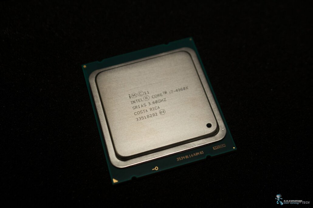 990 mHash/s
 | Name | Meaning |
|---|---|
| PassMark — Single thread mark | 2099 |
| PassMark — CPU mark | 10064 |
| Geekbench 4 — Single Core | 850 |
| Geekbench 4 — Multi-Core | 5157 |
| 3DMark Fire Strike — Physics Score | 6029 |
| CompuBench 1.5 Desktop — Face Detection | 25.225 mPixels/s |
| CompuBench 1.5 Desktop — Ocean Surface Simulation | 174. |
| CompuBench 1.5 Desktop — T-Rex | 0.161 Frames/s |
| CompuBench 1.5 Desktop — Video Composition | 6.883 Frames/s |
| CompuBench 1.5 Desktop — Bitcoin Mining | 32.990 mHash/s |
Features
| Architecture name | Ivy Bridge E |
| Production date | September 3, 2013 |
| Price at first issue date | $999 |
| Place in ranking | 892 |
| Price now | $769. |
| Processor Number | i7-4960X |
| Series | Intel® Core™ X-series Processors |
| Status | Discontinued |
| Price/performance ratio (0-100) | 5.28 |
| Applicability | Desktop |
| Support 64 bit | |
| Base frequency | 3.60 GHz |
| Bus Speed | 5 GT/s DMI2 |
| Crystal area | 257mm |
| Level 1 cache | 384KB |
| Level 2 cache | 1. |
| Level 3 cache | 15MB |
| Process | 22nm |
| Maximum core temperature | 66.8°C |
| Maximum frequency | 4.00 GHz |
| Number of cores | 6 |
| Number of threads | 12 |
| Number of transistors | 1860 Million |
| Unlocked | |
| Maximum number of memory channels | 4 |
| Maximum memory bandwidth | 59. |
| Maximum memory size | 64GB |
| Supported memory types | DDR3 1333/1600/1866 |
| Low Halogen Options Available | |
| Maximum number of processors per configuration | 1 |
| Package Size | 52.5mm x 45.0mm |
| Supported sockets | FCLGA2011 |
| Power consumption (TDP) | 130 Watt |
| Number of PCI Express lanes | 40 |
| PCI Express revision | 3. |