From The Intel Pentium II 350/400 Data Sheet — Intel’s Slot 1 CPUs Uncovered
Skip to main content
Tom’s Hardware is supported by its audience. When you purchase through links on our site, we may earn an affiliate commission. Here’s why you can trust us.
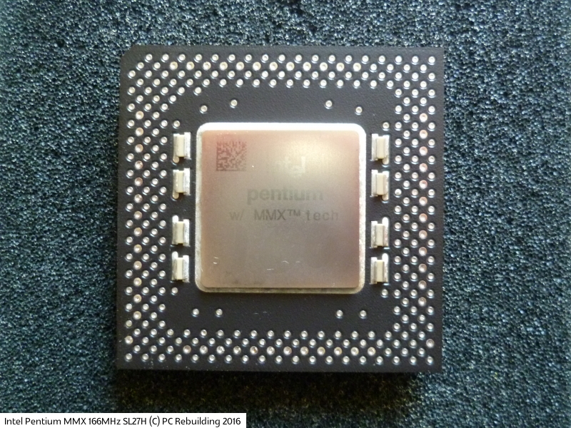
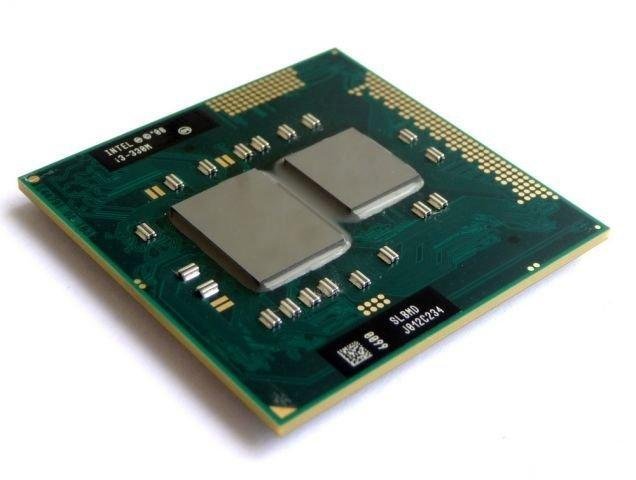
As you can see there’s a serious difference between 333 and 350 MHz Pentium II CPUs and its brothers at 400 MHz. The 400 MHz version has got a different tag RAM chip as well as faster L2 cache modules. 5 ns instead of 5.5 ns seems to sound almost the same, but we shouldn’t forget that 5 ns is about 10% faster than 5.5 ns, which comes close to the increase in core clock or L2 cache frequency respectively of 14% from 350 to 400 MHz. This is not the only difference, the 5 ns L2 cache modules are cooled whilst the 5.5 ns modules in the Pentium 333 and 350 aren’t. This is done via a different back plate of the Pentium II 400 single edge cartridge (SEC), which has two special notches that fit directly on the two modules, as you can see below. The third difference is the timing of the L2 cache. As already said above, the L2 cache timing of the Pentium II 233-300 MHz CPUs is faster than the L2 cache timing of the Pentium II 333. Now the timing of the 5 ns L2 cache in the Pentium II 400 is even slower than in the 333 and 350 models. This is something that should be considered by hardware testers that want to use the easily overclockable Pentium II 333 as test CPU for 400 MHz testing, because the benchmark results scored by this overclocked CPU are higher than what you would get with a real 400 MHz Pentium II.
The latest version of Andreas Stiller’s good old low level benchmark program ‘ctcm.exe’ (published by c’t-Magazine) shows nicely the difference in L2 cache speed. Here are the results of the L2 cache speed at 300 MHz core clock, ran on a Pentium II 300, a Pentium II 333 and a Pentium II 400:
Running each of these CPUs in an application type benchmark like e.g. Winstone shows that at 300 MHz, the Pentium II 400 is scoring considerably less than a Pentium II 300 or 333.
This will also be a pretty nice way of finding out if a 333 or 350 MHz CPU was counterfeit to a 400 MHz model. If ctcm shows 280 MB/s for the L2 cache speed, you can be 100% sure that you’ve bought a counterfeit CPU, opening the CPU and finding 5.5 ns cache will finally prove it.
Overclocking of Pentium II with Deschutes CPUs will in most cases also require the increase of the front side bus, since the higher multipliers will most likely be disabled by Intel. The Pentium II 333 has a multiplier up to 5x built in, so that you can theoretically reach pretty high clock rates, as long as a BX motherboard will let you run this CPU at 100 MHz FSB or even more. Motherboards that detect the FSB clock automatically can only be fooled if you should be courageous enough and change the above mentioned resistors on your CPU PCB. I recommend you rather go for a motherboard that let’s you choose 100 MHz FSB or more regardless what CPU is in there. Overclocking is pretty dangerous when you look at the system stability point of view. Intel has got a good reason for using cooled 5 ns L2 cache modules on their 400 MHz part. The CPU core will in most cases do the higher clock rate just fine, however the L2 cache running at half of this higher clock speed will most likely cause erratic behaviour and can easily be the reason for system crashes. I consider everyone as really crazy, who runs his business software on a system with a highly overclocked Deschutes CPU. Nevertheless, keeping in mind that you can run into system crashes at any time, overclocking works pretty well in the following cases:
- Pentium II 333 to 350/100, careful at 400/100 (requires motherboard that let’s you choose 100 MHz FSB)
- Pentium II 350 to 392/112, possible L2 cache issue, possible PC100 SDRAM issue at 112 MHz
- Pentium II 400 to 448/112, possible L2 cache issue, possible PC100 SDRAM issue at 112 MHz
People that overclock to more than that either post this to make themselves look important without using the system at this speed or they must be considered as a bit crazy. Reaching higher speeds safely only works with special 7 ns SDRAM modules and a Kryotech cooling system as shown by Intel at CeBIT 98, when they presented the 700 MHz Pentium II system.
Current page:
From The Intel Pentium II 350/400 Data Sheet
Prev Page Intel Pentium II 233 — 300 CPUs, Core Codename Klamath
Next Page The Common Core Voltage Of The Deschutes Core Is 2 V
Tom’s Hardware is part of Future US Inc, an international media group and leading digital publisher. Visit our corporate site .
©
Future US, Inc. Full 7th Floor, 130 West 42nd Street,
New York,
NY 10036.
Intel Pentium 350 vs Intel Celeron 2.30
Comparative analysis of Intel Pentium 350 and Intel Celeron 2.30 processors for all known characteristics in the following categories: Essentials, Performance, Memory, Compatibility, Security & Reliability, Advanced Technologies, Virtualization.
Benchmark processor performance analysis: PassMark — Single thread mark, PassMark — CPU mark.
Intel Pentium 350
Buy on Amazon
vs
Intel Celeron 2.30
Buy on Amazon
Differences
Reasons to consider the Intel Pentium 350
- CPU is newer: launch date 8 year(s) 8 month(s) later
- 1 more cores, run more applications at once: 2 vs 1
- A newer manufacturing process allows for a more powerful, yet cooler running processor: 32 nm vs 130 nm
- 16x more L1 cache, more data can be stored in the L1 cache for quick access later
- 4x more L2 cache, more data can be stored in the L2 cache for quick access later
- 3.9x lower typical power consumption: 15 Watt vs 58.3 Watt
| Launch date | November 2011 vs March 2003 |
| Number of cores | 2 vs 1 |
| Manufacturing process technology | 32 nm vs 130 nm |
| L1 cache | 64 KB (per core) vs 8 KB |
| L2 cache | 256 KB (per core) vs 128 KB |
| Thermal Design Power (TDP) | 15 Watt vs 58.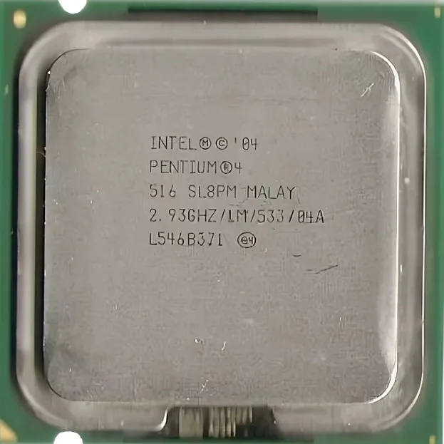 3 Watt 3 Watt |
Reasons to consider the Intel Celeron 2.30
- Around 92% higher clock speed: 2.3 GHz vs 1.2 GHz
| Maximum frequency | 2.3 GHz vs 1.2 GHz |
Compare benchmarks
CPU 1: Intel Pentium 350
CPU 2: Intel Celeron 2.30
| Name | Intel Pentium 350 | Intel Celeron 2.30 |
|---|---|---|
| PassMark — Single thread mark | 559 | |
| PassMark — CPU mark | 227 |
Compare specifications (specs)
| Intel Pentium 350 | Intel Celeron 2.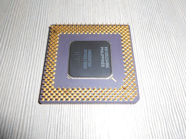 30 30 |
|
|---|---|---|
| Architecture codename | Sandy Bridge | Northwood |
| Launch date | November 2011 | March 2003 |
| Place in performance rating | not rated | 2303 |
| Vertical segment | Server | Desktop |
| Series | Legacy Intel® Celeron® Processor | |
| Status | Discontinued | |
| 64 bit support | ||
| Die size | 131 mm | 131 mm2 |
| L1 cache | 64 KB (per core) | 8 KB |
| L2 cache | 256 KB (per core) | 128 KB |
| L3 cache | 3072 KB (shared) | |
| Manufacturing process technology | 32 nm | 130 nm |
| Maximum frequency | 1. 2 GHz 2 GHz |
2.3 GHz |
| Number of cores | 2 | 1 |
| Transistor count | 504 million | 55 million |
| Base frequency | 2.30 GHz | |
| Bus Speed | 400 MHz FSB | |
| Maximum core temperature | 70°C | |
| VID voltage range | 1.315V-1.525V | |
| Supported memory types | DDR3 | DDR1, DDR2 |
| Max number of CPUs in a configuration | 1 | 1 |
| Sockets supported | 1155 | PPGA478 |
| Thermal Design Power (TDP) | 15 Watt | 58. 3 Watt 3 Watt |
| Low Halogen Options Available | ||
| Package Size | 35mm x 35mm | |
| Execute Disable Bit (EDB) | ||
| Intel® Trusted Execution technology (TXT) | ||
| Enhanced Intel SpeedStep® technology | ||
| FSB parity | ||
| Idle States | ||
| Intel 64 | ||
| Intel® Demand Based Switching | ||
| Intel® Hyper-Threading technology | ||
| Intel® Turbo Boost technology | ||
| Physical Address Extensions (PAE) | 32-bit | |
| Intel® Virtualization Technology (VT-x) |
Navigation
Choose a CPU
Compare processors
Compare Intel Pentium 350 with others
Intel
Pentium 350
vs
Intel
Pentium 967
Intel
Pentium 350
vs
AMD
A8-3520M
Intel
Pentium 350
vs
AMD
A4-3320M
Pentium 350 Processor — Technical City
Intel
Pentium 350
- Interface
- Core frequency
- Video memory size
- Memory type
- Memory frequency
- Maximum resolution
Description
Intel started Intel Pentium 350 sales 21 November 2011.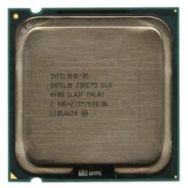 This is Sandy Bridge architecture desktop processor primarily aimed at professional systems. It has 2 cores and 4 threads and is manufactured using 32nm process technology, the maximum frequency is 1200MHz, the multiplier is locked.
In terms of compatibility, this is a processor for the FCLGA1155 socket with a TDP of 15W. It supports DDR3 memory.
We don’t have test results for the Pentium 350.
General Information
Information about the type (desktop or laptop) and architecture of the Pentium 350, as well as when sales started and cost at that time.
| Place in the performance rating | does not participate |
Pentium 350 quantitative parameters such as number of cores and threads, clock rates, manufacturing process, cache size and multiplier lock state. They indirectly speak about the performance of the processor, but for an accurate assessment, you need to consider the results of the tests.
Safety Technologies
Technologies embedded in the Pentium 350 that enhance system security, such as those designed to protect against hacking.
9009 VISTARISETechnologies supported by the Pentium 350 that speed up the operation of virtual machines are listed.
Support1
Integrated video — specificationsGeneral parameters of the graphics card built into the Pentium 350.
Functions
Power consumption
Memory module
Parts and features
Pentium 350 Overclock
Integrated (integrated) graphics
Bus
|
 6 (Xeon Platinum 9221)
  1%
1% 
 2
2
 5 MB/core