Socket M (Intel) | Gough’s Tech Zone
-
My Links
-
Categories
- Audio
- Computing
- DIY
- Electronics
- Event
- Flash Memory
- Lighting
- Obituary
- Opinion
- Photography
- Power Bank
- Radio
- Raspberry Pi
- Salvage
- Satellite
- Tablet
- Tech Flashback
- Telecommunications
- Travel
- Uncategorized
-
Recent Posts
- Quick Review: Lenovo Smart Filament Bulb (G95/E27/806lm, SE-14BEA)
- Salvage: Racal Guardall 10425(?) Passive I/R II Security Motion Sensor
- Tech Flashback: Leadtek My DigiBank 1.5G USB 2.0 Mini External Hard Drive
- Failed, Teardown: Orbit Lighting 2x150W PAR38 Motion Sensor Light (OSLBDIY)
- Quick Reviews: Besign LS10 Laptop Stand & Baseus Orange Dot Wireless Presenter
- Rand(): Equipment Retirements, Tower Upgrade, Scam Calls, Smart Shopping, Rail Strikes & More
- Notes: SSD+RAID Recovery – Samsung 870 EVO Not To Be Trusted!
- Review: VAVA Portable SSD Touch 1TB USB-C (VA-UM004/83-10000-086)
-
Quick Review: Kingston DataTraveler Exodia 32GB USB 3.
2 Flash Drive (DTX/32GB)
- Quick Review: PNY XLR8 CS3030 2TB PCIe Gen3x4 NVMe SSD
- Quick Review: Kingston Fury DDR4 3200MHz 64GB (2x32GB) CL20 SODIMM Kit
- Quick Review: 8BitDo Pro 2 Bluetooth Gamepad
- Quick Review: Sofirn SC21 16340 Li-Ion Flashlight (1000lm/Lh451D/5000K/90CRI)
- Project: Data Recovery from a Blue Imation SuperDisk (LS-120)
- Review: Rohde & Schwarz LCX200 LCR Meter (Overview)
- R&S LCX200 Review – Pt.5: Instrument Performance
- R&S LCX200 Review – Pt.4: Remote Control & Sweep Tool
- R&S LCX200 Review – Pt.3: On the Bench & Documentation
- R&S LCX200 Review – Pt.2: Unboxing & Test Fixtures
- R&S LCX200 Review – Pt.1: LCR Meter Basics & Market Survey
- Tech Flashback: Teletypewriter (TTY/TDD) Calls, Payphones & More
- Random: 5M Views, Vivid Sydney, Flash Memory Fails, Renovation Relics & More
- Project: HP Stream 8 Li-Polymer Cell Cycle Torture Test w/R&S NGM202
- Teardown: Actiiv Wrist Blood Pressure Monitor (ACMMD001) aka Transtek LS810
- Modified: An Annoying Manson HCS-3102 Power Supply Fan Behaviour
- DRW2022 – Pt5: Digital TV (DVB-T), Digital Radio (DAB+) & FM Radio Analysis
- DRW2022 – Pt4: Parap, Jingli, Casuarina, Dripstone Cliffs, Litchfield & Return
- DRW2022 – Pt3: Botanic Gardens, Cullen/Fannie Bay, Nightcliff & Mindil Beach
- DRW2022 – Pt2: Hotel, Darwin CBD and Surrounds, Random Infrastructure
- DRW2022 – Pt1: Getting To Darwin & Travelling Around
- Random: B’day Analysis, element14 Updates, Odd Repairs, Sad Chicken, Free Travel & More
- Teardown: Victron Energy BlueSolar PWM-Pro Charge Controller (SCC010020110)
- Teardown: Winext AN-303 LoRaWAN Temperature/Humidity Sensor
-
Teardown: Simplecom Ch341 4 Port Ultra Compact USB 2.
 0 Hub
0 Hub - RoadTest Review: Keysight Smart Bench Essentials (EDUX1052G, EDU36311A, EDU34450A, EDU33212A)
- Radiofax Update: JFW Ceases Operations, XSG IR Image & Cyclone Charts
- Notes: Rescuing a Box & Downgrading Win10 GPT/UEFI to MBR/BIOS Boot
- Visited: ElectroneX Electronics Design & Assembly Expo (5-6th April 2022)
- Visited: SMB Digital by CeBIT Australia (30-31 Mar 22) & More
- Random: Multiple Webcams & WebRTC, Payphones, Generic SD Cards, Media Appearance & More
- Notes: Cheap Crimps – Weights, Thicknesses & High Current Torture
- Quick Review, Teardown: Creative Live! Cam Sync 1080p V2
- Random: Site Update, Expos, Transport Havoc, Payphones, 3D Printer Fix, Unhappy Meals & More
- Analysis: Australia Unites Flood Appeal Freeview Simulcast (12 Mar 2022)
- Quick Review: Wowstick SD Combo Manual Screwdriver Set (PD01020271)
- Failed, Teardown: Sensirion SPS30 Laser Particulate Monitor Sensor
- *RESOLVED*: Images for posts before 2021 unavailable due to VPS downtime!
- Notes: 3D Printer Filament Spool Weights
- Post-Mortem: A Smoky Triple-Gang Wall Plate Light Switch (Mercury MCC311SW)
- Unbox, Teardown: TP-Link TL-SG105 5-Port Gigabit Desktop Ethernet Switch
-
September 2022 M T W T F S S 1 2 3 4 5 6 7 8 9 10 11 12 13 14 15 16 17 18 19 20 21 22 23 24 25 26 27 28 29 30 -
Archives
- September 2022 (2)
- August 2022 (7)
- July 2022 (11)
- June 2022 (6)
- May 2022 (4)
- April 2022 (9)
- March 2022 (10)
- February 2022 (8)
- January 2022 (6)
- December 2021 (16)
- November 2021 (6)
- October 2021 (8)
- September 2021 (7)
- August 2021 (9)
- July 2021 (7)
- June 2021 (6)
- May 2021 (13)
- April 2021 (13)
- March 2021 (10)
- February 2021 (9)
- January 2021 (12)
- December 2020 (15)
- November 2020 (1)
- October 2020 (9)
- September 2020 (14)
- August 2020 (13)
- July 2020 (7)
- June 2020 (13)
- May 2020 (14)
- April 2020 (18)
- March 2020 (2)
- February 2020 (9)
- January 2020 (21)
- December 2019 (10)
- November 2019 (8)
- October 2019 (14)
- September 2019 (8)
- August 2019 (12)
- July 2019 (9)
- June 2019 (6)
- May 2019 (4)
- April 2019 (12)
- March 2019 (23)
- February 2019 (20)
- January 2019 (23)
- December 2018 (11)
- November 2018 (7)
- October 2018 (4)
- September 2018 (3)
- August 2018 (19)
- July 2018 (6)
- June 2018 (5)
- May 2018 (21)
- April 2018 (7)
- March 2018 (8)
- December 2017 (12)
- November 2017 (19)
- October 2017 (1)
- July 2017 (4)
- June 2017 (16)
- May 2017 (6)
- January 2017 (11)
- December 2016 (30)
- November 2016 (13)
- October 2016 (15)
- September 2016 (19)
- August 2016 (16)
- July 2016 (8)
- June 2016 (31)
- May 2016 (14)
- April 2016 (21)
- March 2016 (13)
- February 2016 (17)
- January 2016 (19)
- December 2015 (20)
- November 2015 (12)
- October 2015 (15)
- September 2015 (4)
- August 2015 (12)
- July 2015 (22)
- June 2015 (14)
- May 2015 (21)
- April 2015 (25)
- March 2015 (14)
- February 2015 (16)
- January 2015 (6)
- December 2014 (11)
- November 2014 (12)
- October 2014 (19)
- September 2014 (11)
- August 2014 (21)
- July 2014 (18)
- June 2014 (20)
- May 2014 (12)
- April 2014 (7)
- March 2014 (23)
- February 2014 (18)
- January 2014 (16)
- December 2013 (15)
- November 2013 (14)
- October 2013 (21)
- September 2013 (13)
- August 2013 (17)
- July 2013 (26)
- June 2013 (26)
- May 2013 (11)
- April 2013 (17)
- March 2013 (31)
- February 2013 (27)
- January 2013 (36)
- December 2012 (31)
- November 2012 (39)
- October 2012 (3)
- February 2012 (18)
- January 2012 (1)
-
Tags
-
Recent Comments
-
Meta
- Log in
- Entries feed
- Comments feed
- WordPress.
 org
org
ASUS CT-479: Socket-478 to Socket-479 Adapter
by Anand Lal Shimpion March 24, 2005 1:31 PM EST
- Posted in
- CPUs
48 Comments
|
48 Comments
IndexASUS CT-479: Socket-478 to Socket-479 AdapterBusiness/General Use PerformanceMultitasking Content CreationVideo Creation/Photo EditingAudio/Video EncodingGaming Performance3D RenderingWorkstation ApplicationsOverclocked PerformanceOverclocked Media Encoding Performance Overclocked Game Performance Final Words
ASUS CT-479: Socket-478 to Socket-479 Adapter
Enter the ASUS CT-479 CPU Upgrade Kit, an adapter board that will convert specific ASUS Socket-478 motherboards to support Pentium M CPUs. You will remember from our original Pentium M desktop article that the pinout of the Pentium M is different than the Pentium 4, although the two chips are electrically compatible (they use the same FSB). The next problem is that the Pentium M relies on a much lower voltage version of the Pentium 4’s FSB, which is also addressed by ASUS’ adapter, a problem that we did not think was solvable until now.
The CT-479 only works with ASUS motherboards, and only a limited number of them at that. Currently, only the ASUS P4P800-SE and P4P800-VM motherboards are supported, both of which are i865 based motherboards. ASUS is working on support for other boards; the P4C800-E (875P) will be supported soon. For our tests, we used a P4P800-SE; you need a BIOS update, but that’s all. Obviously, non-ASUS motherboards are not supported; however, we’re not certain whether or not the adapter can be made to work in other boards. We will be looking into this as time goes on, but we wanted to make sure that we could complete this article first before doing anything that would damage our setup.
The CT-479 supports all Pentium M and Celeron M CPUs (Dothan and Banias based) with the exception of the Low Voltage and Ultra Low Voltage versions.
The jumpers switch between 400 and 533MHz FSB settings. The power connector powers the adapter.
The CT-479 comes with the adapter board, heat sink/fan and power cable.
A perfect fit
The supplied heat sink is specifically made for the CT-479.
Currently, ASUS is listing the CT-479 as a part of a bundle with the P4P800-SE, priced at $130. At that price, the solution is almost half the price of the AOpen/DFI motherboards, and you get all of the benefits of the 865 chipset. The main benefit of the 865 chipset in this case is its dual channel DDR400 memory controller. The 533MHz FSB Pentium Ms are memory bandwidth starved by the 855GME’s single channel DDR333 memory controller, so being paired with an 865 gives the CPU more memory bandwidth than it can use.
The P4P800-SE that we tested only allowed for 5:4 and 1:1 memory clock speed ratios, meaning that for our 533MHz FSB Pentium M, the maximum stock memory clock was DDR333.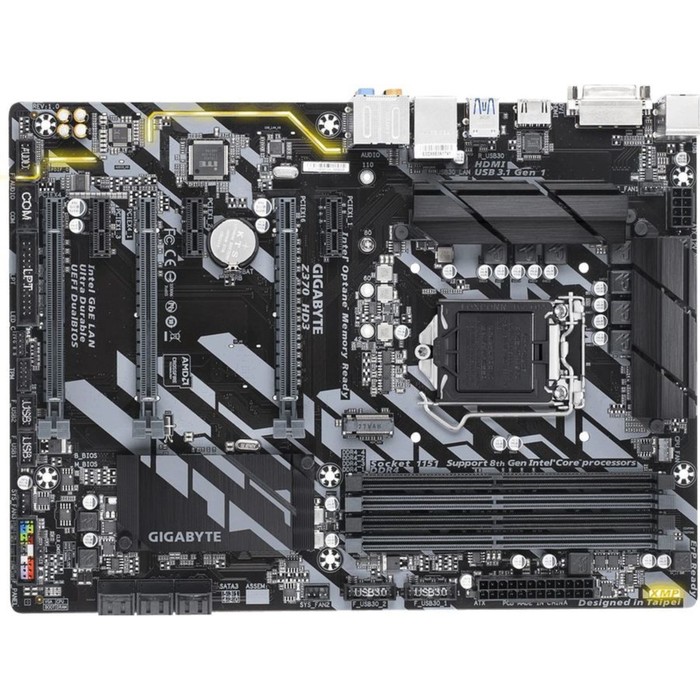 But since we’re talking about a dual channel memory controller, even at DDR266 speeds, you have enough memory bandwidth for the processor — DDR400 support isn’t necessary.
The other major benefit of the CT-479 is that you get to use a mature, mass-produced ASUS motherboard instead of a smaller production run, recently released 855GME solution. The benefits were clear in our testing — overclocking the Pentium M was far less of an ordeal on the ASUS solution.
The CT-479 does not support the Pentium M’s SpeedStep technology, which has a handful of implications:
1) System power consumption will be higher on the ASUS solution than on 855GME based systems from AOpen/DFI. The reason being that the CPU will always run at maximum frequency, which is still lower power consumption than any other desktop processor, but it is worth mentioning.2) You can’t adjust the clock multiplier of the Pentium M like you can on the AOpen/DFI offerings. This will hamper the more adventurous overclockers, but it’s definitely not a show stopper.
You also can’t adjust the Pentium M’s core voltage when using the CT-479; you’re stuck at the default voltage. ASUS’ Q-Fan technology (which allows for the automatic reduction of fan speed depending on thermal load) is supported, so you can reduce noise output even if SpeedStep isn’t supported.
ASUS just announced the CT-479 last week, so there are some details that aren’t yet available, such as whether or not the kit will be offered outside of the ASUS motherboard bundle. As soon as we have this information, we’ll pass it along, but even if the only way to get it is with an ASUS motherboard, it is still a much better value than a standalone Pentium M motherboard.
The question here is how big of an impact does the 865 chipset have on the desktop performance of the Pentium M? To find out, we paired it with the Pentium M 770, Intel’s fastest Pentium M running at 2.13GHz. The Pentium M 770 requires a 533MHz FSB, which is supported by the 865 chipset, and thus, is also supported by the CT-479 upgrade kit.
The Test
Our hardware configurations are similar to what we’ve used in previous comparisons.
AMD Athlon 64 Configuration
Socket-939 Athlon 64 CPUs
2 x 512MB OCZ PC3200 EL Dual Channel DIMMs 2-2-2-10
NVIDIA nForce4 Reference Motherboard
ATI Radeon X800 XT PCI Express
Intel Pentium 4 Configuration
LGA-775 Intel Pentium 4 and Extreme Edition CPUs
2 x 512MB Crucial DDR-II 533 Dual Channel DIMMs 3-3-3-12
Intel 925XE Motherboard
ATI Radeon X800 XT PCI Express
Intel Pentium M Configuration
Intel Pentium M 725 — 755
2 x 512MB OCZ PC3200 EL Dual Channel DIMMs 2-2-2-10
AOpen GMEm-LFS Motherboard
ASUS P4P800-SE + CT-479 Adapter
ATI Radeon X800 XT AGP
Index
Business/General Use Performance
IndexASUS CT-479: Socket-478 to Socket-479 AdapterBusiness/General Use PerformanceMultitasking Content CreationVideo Creation/Photo EditingAudio/Video EncodingGaming Performance3D RenderingWorkstation ApplicationsOverclocked PerformanceOverclocked Media Encoding Performance Overclocked Game Performance Final Words
Tweet
PRINT THIS ARTICLE
MB899 Mini-ITX Motherboard with Socket M
Embedded Computer Products
-
SPECIFICATIONS
Out of stock
MB899 Mini-ITX Motherboard with Socket M quantity
-
SPECIFICATIONS
Latest Articles
Featured Article
5 Factors to Consider Before Buying an Industrial PC
Choosing the right embedded system to power your industrial application is crucial. To help you make the correct decision, here are 5 things to keep in mind when you are shopping for an Industrial PC. 1: Longevity Product lifecycles can be tricky. It is common to pick an older processor to save costs, only for […]
View Article
Company News
-
5 Factors to Consider Before Buying an Industrial PC
September 15, 2022
Choosing the right embedded system to power your industrial application is crucial. To help you make the correct decision, here are 5 things to keep in mind when you are shopping for an Industrial PC. 1: Longevity Product lifecycles can be tricky. It is common to pick an older processor to save costs, only for […]
View Article
-
PCIe Gen 4 Explained
July 11, 2022
The Peripheral Component Interconnect Express or PCIe as it is usually known is the most powerful interface for installing additional components on a motherboard.
 Offering higher data transfer rates than any other serial bus, PCIe ports are the preferred means for attaching expansion cards like a GPU or a Wi-Fi card. And like any other […]
View Article
-
Uses For Medical Tablets
June 20, 2022
-
Is SSD Always the Better Option?
April 15, 2022
View All News
From the Blog
-
A Crash Course to PCIe Gen 5.
 0
0 September 7, 2022
Motherboards supporting PCIe Gen 5.0 have just started hitting the shelves, and it won’t be long before graphic cards and SSDs taking advantage of the speed boost follow suit. Let’s find out what’s changed in the new standard. An Introduction to PCI-Express Peripheral Component Interchange Express or PCIe is the technology that enables you to […]
View Article
-
What to Do When Your Chipset Reaches End-of-Life
August 22, 2022
End-of-Life (EOL) is probably the most dreaded word for any business owner.
 No one wants to suffer delays in their work when their setup is rendered obsolete by an EOL declaration by the manufacturer. But what exactly does EOL mean? Do you really have to switch technologies? How can you plan ahead to avoid losses? […]
View Article
-
Giada DK310 Digital Signage System
August 10, 2022
-
What is Better – Panel PC or Rugged Box PC with Touch Screen Display?
July 26, 2022
View all Blogs
AMD AM5 Socket: Everything You Need to Know
AM4 Socket seems dead and buried with the release of new Zen 4 CPUs on AMD AM5 Socket. It was the AMD’s previous flagship socket, the foundation for all Ryzen processors from the very first to the brand new Ryzen 7 5800X3D, released a few months ago. Back in September 2016, AMD introduced the AM4 Socket. Starting with Zen+ and continuing through Zen 3, AMD has relied on it as the foundation for its various microarchitectures.
The AMD Ryzen 7000 Series Desktop CPUs are powered by the new Zen 4 microarchitecture. With the release of the AM5 Socket, the AM4 era has come to an end. After AM4’s enormous success, it has some large shoes to fill. More options become available when upgrading to a new chipset. AMD will continue to support the new AM5 CPU socket until 2025. With the release of the AMD Ryzen 7000-series CPUs, AMD has introduced its first new processor socket in six years and its first LGA design.
While the AM4 Platform will continue to be supported for the foreseeable future, gamers, developers, and workstation users should start thinking about the future. Consequently, Ryzen 7000 series processor will outshine the competitors from the new features and increase the performance of the AMD AM5 Socket and 600-series chipsets that AM5 boards will include.
On the contrary, a slew of issues about technology tension has arisen with the release of the AM5 Socket and the subsequent processor lineup. We will discuss some considerations if you are attempting to move to a new platform and its possible difficulties. This article will cover all the details, such as Zen 4 architecture, how AM5 is superior to AM4, the new Ryzen 7000 CPUs, and many more.
Table of Contents
Introduction to AM5 Platform
AM5 Platform
Uncertainty on the user’s side is standard when upgrading to a new CPU, motherboard, or another component. After five years of dependable service on the AM4 Platform, AMD decided to upgrade to AM5. The moment has come, and we must choose. The AM5 Platform offers many new features and opportunities for users of all stripes.
Whether they’re gamers, creators, or anything in between. The previous AM4 motherboards might often be made to run the newest CPUs by just updating their BIOS. As the market shifts to more contemporary standards like DDR5, AMD is being forced to react, so they have released a new socket platform called AM5 to go along with its Zen 4-based Ryzen 7000 CPUs.
The AMD Ryzen 7000 series, based on Zen 4 architecture, uses the new AM5 socket type. The AM5 and Zen 4 will be launched on September 27th, corresponding with Intel’s Raptor Lake reveal. It was announced during AMD’s “Together we progress PCs” event on August 29th, 2022.
They are beginning with the Zen 4 microarchitecture. AMD Ryzen microprocessors will use the AM5 LGA 1718 CPU socket. AM5 is AMD’s first LGA socket built for mainstream enthusiast CPUs. The transition from the AM4 to the AM5 socket type among PC enthusiasts will be led to considerable perplex.
Even though AMD announced the new AMD AM5 Socket in January 2022, they remained tight-lipped regarding the Socket’s specifications at the time. However, as time has progressed, more details regarding the Socket have been revealed. We can now claim that the AM5 Socket offers a plethora of advancements. So, what are the changes associated with the AM5 Socket and its additional features? In the following parts, we’ll dive further into this.
Support For DDR5 Memory Only
Support For DDR5 Memory Only
AMD has been teasing us for so long that the new AM5 Socket and the upcoming Ryzen 7000 will use the recent industry standard DDR5 memory, which is more efficient and faster. Finally, AMD has revealed that the AM5 Socket would be AMD’s first DDR5-based Platform. The new AM5 Platform is a radical departure from AM4 regarding design philosophy and feature set.
It doesn’t simply deliver the usual dose of performance gains that we see every iteration. Henceforth, we are witnessing a considerable performance shift from the previous Generation, like the inclusion of DDR5 memory. AMD’s AM5 Socket does not have support for DDR4 memory. In contrast to Intel’s LGA 1700 socket.
Therefore, the Ryzen 7000 and subsequent AMD CPUs will only be able to use DDR5 memory. This guarantees the fastest potential performance for systems using the AM5 Socket. It will increase the build cost since DDR5 is more costly than DDR4. In addition, DDR4 RAM isn’t physically compatible with DDR5 slots. Thus updating your PC will need purchasing new DDR5 RAM modules.
The AM5 Socket does not support DDR4 memory because the new memory type, DDR5, has an integrated voltage controller and hence needs a different pin arrangement. Consequently, this shift may be essential since it is sometimes inconvenient to build numerous boards for various memory kinds. AM5 Socket can drive the most PCIe Gen 5 lanes from the CPU socket and supports next-generation IO features like dual-channel DDR5 memory.
AMD recommends DDR5-6000 memory for use with their Zen 4-based Ryzen 7000 CPUs. Like its predecessors, it has a memory configuration that delivers optimum gaming performance and latency-sensitive tasks. Many of us may feel that upgrading to DDR5 is unnecessary or too costly at this time. But the days are coming when DDR5 memory will be standard.
New LGA 1718 Socket
New LGA 1718 Socket
The dust has settled following the transition to the new memory and PCI 5.0 standards. AMD has also jumped to a new socket standard. Regarding the AM5 Socket, AMD is finally moving away from the PGA interface used by socket AM4 and adopting the more standard LGA interface. This is a significant shift for AMD, which relied on the PGA interface for a better decade.
While we were still utilizing Pentium 4 CPUs, Intel made this change for its processors back in the LGA775 era and hasn’t looked back since. After being released in 2016, AM4 needed to be updated. They required extra pins to use PCIe Gen 5, so they switched to LGA Socket. A land grid array in which the pins are located on the motherboard rather than the CPU. And second, DDR5 memory. More power would generate, and the signal integrity of all high-speed I/Os will be improved, thanks to the switch.
As a result, enhancements were generally required. This is an excellent explanation for why AM4 does not support DDR5 memory. After all, the LGA 1718 is 18 times more advanced than the LGA 1700 used by Intel’s 12th Generation. Once again, AMD is in the first place. AM5 has 1,718 pins, significantly increasing over AM4’s 1331 pins. This is made possible by the increased pin count of the LGA socket.
Since the pins are located on the motherboard, this might increase the price, as we have seen with specific Intel boards. Experts in the field contend that consumer demand has driven the shift toward LGA. CPU contact pins are substantially more vulnerable than motherboard pins, making CPUs more susceptible to damage. Moving to an LGA-type socket may not result in any noticeable performance improvements. However, the different pin arrangements have their benefits.
AMD’s RDNA 2 Graphics
AMD’s RDNA 2 Graphics
Sony’s PS5 and Microsoft’s Xbox One S all use AMD’s RDNA 2 graphics architecture. The revolutionary RDNA architecture debuted at E3 2019 and has since been at the forefront of developing cutting-edge hardware for immersive, high-performance gaming. The genetic code that drives your games, the substance that gives them personality, and the continuously tweaked and improved component.
The connection between AMD and integrated graphics in the Ryzen era has been sporadic. The original Ryzen CPUs did not have integrated graphics. Although, AMD later released the 2400G and 2200G, which swapped some of the CPU cores for Vega graphics. However, most of AMD’s high-end desktop CPUs have never integrated graphics and instead relied on separate graphics cards. Unlike Intel, whose CPUs often have some integrated graphics. AMD’s processor could not give display without a particular graphics card.
It seems that AMD’s Zen 4 Ryzen 7000-series CPUs will follow Intel’s lead and include RDNA 2 graphics. Currently, all AM5-compatible CPUs have built-in graphics. The Steam Deck portable console, which has an 8-core RDNA 2 graphics processor, is a prime example of the superiority of AMD’s RDNA 2 graphics. Thus this is a piece of welcome news.
The new and improved compute unit, visual pipeline, and AMD Infinity Cache included in the AMD RDNA 2 architecture make it possible for high-resolution video games to have crisp, detailed images, regardless of the game’s screen size. Not a robust solution, but it might be able to run recent 1080p games. Ryzen 7000 may have graphics performance on par with the dedicated Radeon RX 6400.
Supported Chipsets
AM5 Supported Chipsets
The shift to the AM5 platform ecosystem is one of the most exciting features of AMD’s newest product line, even more so than the CPU itself. The longevity and capabilities of the AM4 Platform were far beyond our wildest expectations when it was initially released. Many of the same driving principles were applied to the new chipsets when they were being designed.
AMD’s goal in developing this new Platform was to make it as adaptable and future-proof as possible. One that makes the most of what the latest Ryzen 7000 series CPUs offer. It would have the modern I/O and interfaces that would characterize the next Generation of enthusiasts’ desktop computers. For the most demanding PC setups, we believe the upcoming AM5 Platform will be the benchmark.
DDR5 compatibility, 24 ultrafast PCIe lanes capable of gen five speeds, and 14 super speed USB ports boasting 20GB/s speeds are just a few of the cutting-edge technologies the new motherboards will provide. This, according to AMD, allows them to provide manufacturers with a variety of connection choices while still concentrating on the fabrication of a single chip to maximize efficiency and output.
The X670E, X670, B650, and B650E are the four AM5 chipsets that have been disclosed so far. Like the present Generation, these new motherboards will naturally come equipped with various functions aimed at consumers. The X670 and X670E chipsets will be the first to be released on September 27th. They will be followed by the recently announced B650E and B650 in October.
AMD X670E Chipset
In situations when only the absolute quickest will do, an AMD X670E motherboard is the way to go. Motherboards based on the AMD X670 chipset are the absolute pinnacle of performance. The most discerning enthusiasts may be sure that these motherboards provide nothing less than the absolute pinnacle of performance in every conceivable respect. With PCIe 5 compatibility for graphics and NVMe as well as two-channel DDR5 memory, boasting the most extreme overclocking headroom and the most power phases.
They can push the envelope of performance and overclock to new heights. With the incredible performance of an AMD X670E motherboard and AMD Ryzen 7000 Series CPUs, you can play the most demanding games and complete the most challenging tasks. It supports up to four DisplayPort 2.0 and HDMI 2.1 inputs. All of the X670E’s PCIe slots (primary, secondary, and M.2) can be connected to a PCIe 5. The X670 Extreme is said to feature unfettered overclocking because of its abundance of VRMs and superior power staging and delivery. Because of its superiority, the X670E is likely to be rather expensive.
AMD X670 Chipset
After that, the X670 Platform has everything most Ryzen gamers need. The X670 only supports PCIe GPUs in its primary X16 PCIe slot. The remainder of its PCIe slots only supports PCIe Gen 4. The board also has very robust memory overclocking and CPU power delivery. The X670 chipset is identical to the X670E connection but has less functionality. However, the X670 may not provide nearly as much delivery support, but it still supports overclocking to the levels expected by enthusiasts.
The X670E and X670 motherboards use PCIe Gen 5 to power M.2 storage. Thus this isn’t changing. The motherboard using the X670 chipset is expected to be slightly lower than the X670E price. The X670 chipset will be used in most mainstream high-end motherboards and available in various models with varied PCIe compatibility. This provides an affordable tier of PCIe 4.0 X670 motherboards, enabling enthusiasts to save money by not switching to PCIe 5. 0.
0.
AMD B650 Chipset
In a nutshell, B650 boards provide an excellent compromise between cost and performance. These motherboards are tailored to performance users interested in the complete set of features available in the AM5 ecosystem. Still, they don’t necessarily need the extreme overclocking capabilities of the X series boards. To fully use what Generation 5 has to offer, B650 chipset boards will have PCIe 5 to M.2 storage connections if you’re looking for balanced performance from your board.
DDR5 memory, AMD EXPO tech, and PCIe 5.0 for an NVMe SSD are here to usher in the next era. The AM5 motherboard with the B650 chipset is priced more affordably with no provision for overclocking. The B650 will almost certainly contain less powered VRMs than its superior counterparts. There will be just one chip on the motherboard that makes up the B650 chipset.
Although AMD hasn’t said it, we may guess that the company is pushing toward PCIe 5.0 speeds to boost the bandwidth between the CPU and chipset. In this case, Intel’s utilization of an eight-lane DMI connection is preferable, even though AMD could achieve the same total bandwidth with a PCIe 5.0 link utilizing just four lanes.
AMD B650E Chipset
Finally, the AMD B650E strikes a delicate balance between supporting next-generation technologies and providing excellent value to the end user. An AMD B650E motherboard is a must-have if you are a serious gamer or creator. The NVMe disk you use will be supported by PCIe 5.0. Likewise, the DDR5 memory you use will use AMD EXPO technology. The in-game performance-boosting capabilities of the AMD B650E are many.
The B650E chipset allows motherboard manufacturers and ends users to choose a more affordable platform without losing the reliability or scalability of PCIe 5.0. PCI Express 5.0 lanes necessitate a higher-quality PCB, often with extra layers that enable the tracks to maintain signal integrity at cost. Because of the B650E chipset, manufacturers may employ PCIe 5. 0 laning, which is more costly, with lower-priced controllers.
Therefore, reducing overall costs. Ultimately, this implies that AMD will provide two distinct platforms. The high-end B650E comes standard with PCIe 5.0 lanes. Consequently, the more affordable B650 uses PCIe 4.0 lanes just for the PEG and M.2 slots. One of the primary advantages of AMD’s AM5 Platform is the inclusion of at least one PCIe 5.0 M.2 storage slot on most boards.
PCIe Lane
PCIe 5.0 is used by the AM5 Socket, which offers double the data transfer speed of PCIe 4.0. This will enable you to take advantage of the rapidly improving SSDs currently marketed. PCIe 5.0 allows for faster data transfers and the use of cutting-edge tools. The great thing about PCIe is that it is fully compatible with the previous Generation.
Your new AM5 socket motherboard and Ryzen 7000 CPU will be compatible with your existing PCIe 4.0 SSDs and GPUs. All 28 of the Zen 4 CPU’s PCIe lanes are PCIe 5.0. There will be one x16 PCIe slot, or the first 16 PCI Express lanes may be divided in half to provide two x8 PCIe slots. Since AMD only mandates PCIe 5.0 on the X670E boards, cheaper motherboards may support PCIe 4.0.
At least four of the eight GP lanes on the new Zen 4 Ryzen CPUs must be used for an M.2 storage slot. Motherboard manufacturers are responsible for implementing the remaining four lanes. Specific boards will use these to support Thunderbolt 4 and USB4. These lanes may be utilized for a second M.2 expansion slot if the other choices aren’t needed. AMD showed off a variety of AM5 chipset alternatives, each of which seemed to be a unique design built on its silicon.
AMD and ASMedia collaborated to develop a single chipset, Promontory 21, that is usable in various setups. The X670 and X670E include two B650 chipsets daisy-chained together to increase the number of available connections. We can’t predict how it will affect performance anytime soon. There is practically any performance gain from PCIe Gen 3 to PCIe Gen 4, even with today’s most powerful GPUs.
AMD AM5 CPU Cooler Compatibility
AMD has confirmed that AM4 coolers may be used with the new AM5 Socket. As a result, consumers may keep using the same cooling systems for their existing AM4-socket CPUs even after upgrading to a Ryzen 7000 processor. The cooling system for the Ryzen 5000 series will likely be enough for the 7000 series, given that you are upgrading to a processor of the next level since AMD states that the Ryzen 9 7950X is 47% more energy efficient than the 12900K.
Several manufacturers of CPU coolers have said that their AM4 models are upwardly compatible with the AM5 Socket, making them suitable for use with Zen 4 CPUs. According to Noctua, the NH-L9a-AM4 and the NM-AM4-L9aL9i are the only Noctua coolers and mounting kits that are not upwardly compatible with socket AM5. Except for them, all Noctua AM4 coolers mountings screw into the threads of the standard AM4 stock backplate.
Their AM4 mountings that connect to the standard AMD backplate are compatible with AM5 as well since the threads and pattern on the backplate are the same in both cases. Cooler Master, on the other hand, displays all of its air- and liquid-cooling solutions that work with the modern AM5 Platform. However, not all of them will work right out of the box.
Source: Cooler Master Website
What’s New in Zen 4 Architecture
Zen 4 Architecture
The Zen 4 architecture using five nanometers is the foundation of AMD’s AM5 Socket. For example, TSMC uses a finFET fabrication method, the fourth Generation. This is a 3D fitting system. AM5 uses DDR5 memory and operates on PCIe 5. It has graphics that cannot saturate the PCIe lanes. PCIe Gen 4 supports read/write speeds of up to 5 gigabytes per second.
In November of 2022, PCI Express Generation 5 drives will be available. PCIe Gen 5 is great since it will provide unprecedented bandwidth and throughput for drives. PCIe Generation 5 is already available on Intel hardware. It’s great to see so much cutting-edge innovation happening over at AMD.
The next-generation AMD Ryzen 7000 desktop CPUs combine the company’s new Zen 4 core in 5nm manufacturing technology with the brand-new AM5 Socket architecture to increase desktop PC’s performance, features, and capabilities.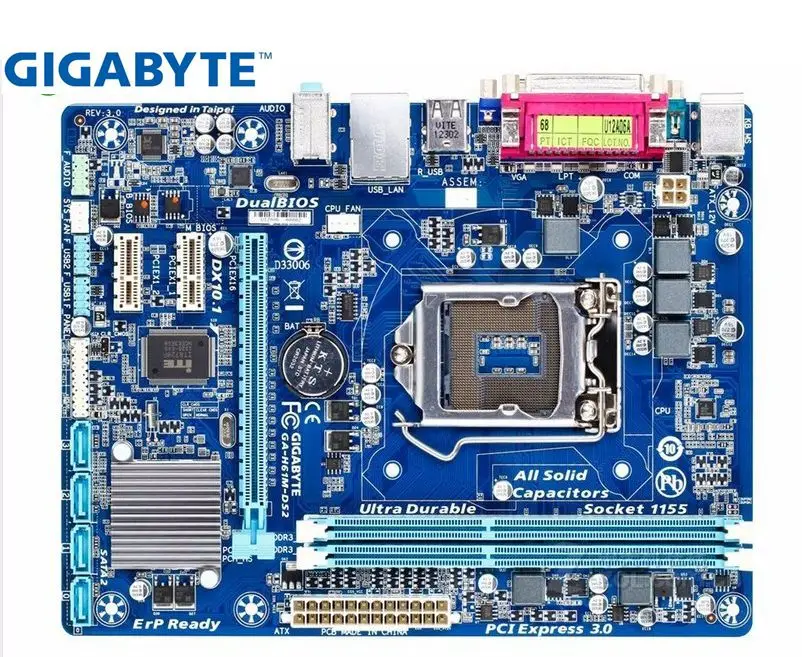 The foundation is the Zen 4 CPU at its heart. AMD plans Zen 4 core to improve upon the already impressive performance and performance per watt of the Zen 3 core.
The L2 cache capacity has doubled per core from 512 KB to 1 MB. The clock speed of Zen 4 is now significantly over 5 GHz. We also anticipate that Zen 4 CPUs will provide more than 15% greater single-threaded performance than previous generations, thanks to increased IPC and clock speed. AMD also included directives for AI workloads that may take advantage of hardware acceleration, such as neural networks and machine networking.
First 5nm x86 Processors
First 5nm x86 Processors
There are up to two chiplets in the new Ryzen 7000 series CPUs, each of which has eight Zen4 cores fabricated using an enhanced version of TSMC’s potent five-nanometer manufacturing technology. A brand-new I/O die built just for Ryzen 7000. The bigger chiplet is manufactured at a reduced manufacturing node of only six nanometers.
With the addition of RDNA 2 graphics, AMD has finally included integrated graphics in its Ryzen desktop CPUs.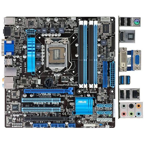 Power management has improved, and new IO and memory standards, including DDR5 and PCIe 5, are supported. With 5nm, AMD’s partnership with TSMC and its AID partners, which dates back a decade, will continue.
AMD’s optimization of scaling, device capacitance, and metal stack considerably aided in Zen 4’s performance. They cut the Di area by another 18% by downsizing the size and the physical space. Despite including improved performance features. To achieve high efficiency and high density in routing, a 15-layer telescopic metal stack has been jointly optimized.
With each successive Generation, AMD maintains its dedication to low power consumption without sacrificing performance. Their innovation in technology includes a 20% decrease in device capacitance and advancements in design as critical enablers. Zen 4 is 62% more efficient at the same performance level and 49% more powerful while using the same amount of power.
AMD’s high-performance CPUs will have a minimal effect on the environment, which is a priority for the company. This is quickly becoming an essential factor for many of their customers. The transition from the Zen 4 to the Ryzen 7000 series is reflected in the performance benefits seen throughout the TDP spectrum. Due to the massive increases in IPC, this impact is magnified.
AM4 vs. AM5 Platform
AMD has released the new AM5 Socket for its upcoming Ryzen 7000 CPUs. But what are the main changes between it and AM4, and should you upgrade? Let’s get into the specifics here. And although AM4 is an excellent platform that will be around for a long time, designing the finest PCs is always about breaking barriers. Therefore, AMD integrates its multi-generational CPU core roadmap with comments on its cutting-edge production processes and industry-leading packaging innovations.
Since the AM4 Socket from the previous Generation has a maximum TDP of 142 watts, CPUs based on the Zen 3 Architecture can only achieve 105 watts TDP. However, with the introduction of the AM5 Socket, AMD could increase its maximum capacity to 230 watts, enabling the newest Ryzen 7000 CPUs to have a maximum TDP of 170 watts. AMD may leverage the improved power supply to develop more powerful CPUs. Therefore, the AM5 Socket can support even the most powerful CPUs AMD develops in the future.
The AM5 Socket adopts Intel’s land grid array (LGA) instead of PGA. AMD claims it is required to handle DDR5 memory and PCI Express 5.0. Therefore increasing the contact density on the same package was a priority. Additionally, the AM5 Platform is praised for its enhanced signal integrity and cutting-edge connection capabilities, including its support for dual-channel DDR5 memory, compared to its predecessor’s sole support for DDR4.
Up to 24 PCIe5.0 lanes are available on the AM5 Platform, making it AMD’s most feature-rich desktop platform to date. With AMD’s platform lifespan until 2025 and beyond, consumers can expand with their Socket AM5 solution thanks to supporting new and developing technologies like PCIe Gen 5 and DDR5 memory.
AMD Ryzen 7000 Series Processors
AMD Ryzen 7000 Series Processors
The AMD Ryzen 7000 Series continues the “Zen” architecture’s track record of innovation, execution, and delivery with another double-digit increase in IPC above “Zen 3”. The Ryzen 7000 Series is the first high-performance x86 5nm CPU, ushering in the lightning-fast “Zen 4” architecture to take gaming and content production to new heights.
The top-of-the-line 16-core AMD Ryzen 9 7950X CPU provides up to 57% greater content production performance in V-Ray Render than competing systems. Meanwhile, even AMD’s 6-core Ryzen 5 7600X CPU is, on average, 5% quicker in gaming performance across a selection of games compared to the competition’s top gaming processor.
Stunning increases in energy efficiency accompany the tremendous performance enhancements; the AMD Ryzen 7950X CPU is up to 47% more energy efficient than the competition. The Ryzen 7000 Series Processors, include a whole new 6nm I/O chip that accelerates hardware-based video encoding and decoding, light-duty graphics processing, and multiple monitor compatibility.
Ryzen 7000 Series Desktop CPUs operate more effectively than ever, thanks to various innovative power management features borrowed from AMD’s ultra-efficient mobile processors. On September 27th, 2022, the first batch of four Zen 4 Ryzen 7000 CPUs will be released. You can get your hands on the premium X670 and X670E chipsets at release. The more affordable B650E and B650 chipsets won’t come until October.
However, PCIe 5.0 SSDs won’t be released until October, but DDR5 memory kits will be available at launch. For the Ryzen 7000 CPUs, TSMC’s N5 5nm manufacturing node is used for the core computing die, while TSMC’s 6nm process is used for the I/O Die. No graphics-free variants of the Ryzen 7000 processor will be available. They are supported by the RDNA 2 engine, which is located on the IOD (I/O Die).
Ryzen 9 7950X
Ryzen 9 7950X
AMD’s 16-core, $699 Ryzen 9 7950X flagship processor is billed as the world’s fastest CPU. With the high-end 7950X, AMD competes head-to-head with Intel’s CPUs and says it is 11% quicker overall in gaming compared to Intel’s fastest chip, the 12900K. The Ryzen 9 7950X, with its 16 cores and 32 threads, costs $100 less than its predecessor, the Ryzen 9 5950X.
The flagship Ryzen 9 7950X will have a clock rate that is 16% higher than the Ryzen 9 5950X, with a boost clock rate of 5.7 GHz. This outstanding accomplishment for a 16-core processor represents the highest frequency increase in the Ryzen era by 800 MHz. Although AMD’s top-of-the-line 16-core Ryzen 9 7950X is priced competitively, the $100 premium for the Ryzen 7 7700X seems excessive. The persistent expensive cost of the base model is another potential turnoff for fans.
Ryzen 9 7900X
Second Strongest Ryzen 7000 Series Processor
Like its predecessor, the Ryzen 9 5900X, the Ryzen 9 7900X has the same starting price for its complete set of 12 cores and 24 threads. Also noteworthy is that Ryzen 9 7900X boasts a significant 800 MHz increase in clock speed across its 12 cores. AMD has verified that Ryzen 7000 still has Precision Boost 2 to reveal the most significant boost frequencies available at all times. However, this will only happen on two cores.
Ryzen 7 7700X
Ryzen 7 7700X
However, AMD’s eight-core, 16-thread Ryzen 7 7700X has a $100 higher starting price than the 5700X.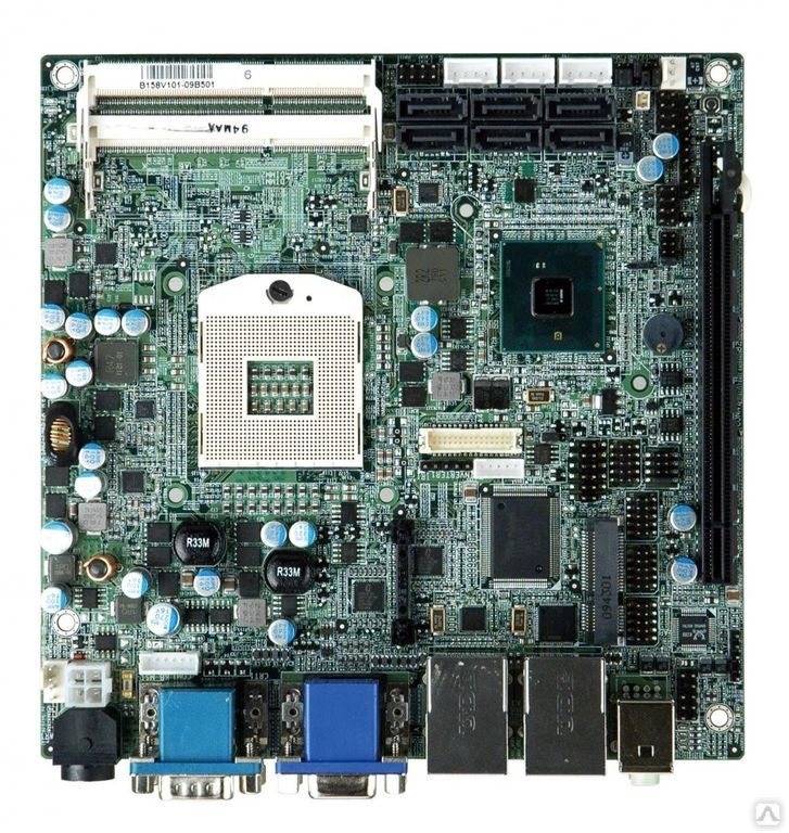 There is no change to the TDP of the Ryzen 7 7700X. Furthermore, the AM5 Socket’s PPT maximum power consumption has increased to 230W. This is a substantial improvement compared to the previous-generation Ryzen 5000’s maximum power consumption of 142W.
Ryzen 7 7700x with eight cores of its own, the Zen 4 processor outperforms the Ryzen 7 5800X by a staggering 32% in the multi-threaded Cinebench test. The $100 extra for the Ryzen 7 7700X seems excessive. The persistent expensive cost of the base models is another potential turnoff for fans.
Ryzen 5 7600X
Ryzen 5 7600X is the entry-level model of AMD’s Zen 4 CPUs. Based on AMD’s internal testing, these processors will provide industry-leading performance, marking a welcome return to form. The 12900K is inferior to even the budget Ryzen 5 7600X by 5% in gaming performance. The chips also include cutting-edge technology. Such as a new integrated Radeon RDNA 2 graphics engine and support for AVX-512-based AI instructions.
Although it’s great that AMD has maintained the $299 price point for the entry-level Ryzen 5 7600X, it’s not a full victory since this same high entry-level pricing was criticized when the Ryzen 5000 series was first released. AMD claims that the highest performance gains may be seen in the lower TDP levels when using the Zen 4 architecture in conjunction with the TSMC 5nm node. That makes logical, as there are always some sacrifices in power and performance as you go up the frequency/voltage curve.
Ryzen 7000 Features and Performance Improvements
So, we’re talking about AMD’s next AM5 Platform and the Ryzen 7000 family of processors. Since the AM4 Socket had been in use since 2016, a revamp was in need. Come, let’s discuss the IPC. They conducted extensive testing across the board, resulting in an average IPC uplift of 13%. Like most enthusiasts who conduct IPC comparisons, AMD capped the clock speed at four different types.
They were able to synchronize the frequencies of the 5950x and 7950x, resulting in a median performance boost of about 13%. It reached 39% in one area to the max and 1% in another at the lowest. What’s crazier is that AMD can achieve it with a relatively simple and practical approach. Now, the TDP is 170 watts, an upgrade over the 5950x, which presently displays 105.
AMD had to elevate that TDP since it has a boost of up to 5.7 GHz on the 7950x. Nowadays, single-core speed is crucial in applications like Adobe. Believe it or not, many adobe processes are still single-threaded. So, 5 to up to 5.7 GHz per core is a significant boost. This is higher than Intel’s single-core boost clock, an area in which Intel has traditionally excelled. AMD’s actual clock speed has now surpassed Intel’s, and the day has finally arrived.
Because of how modern Silicon technology is produced, we once believed that it would be impossible to achieve speeds of five gigahertz or higher. Incredibly, we can produce chips using a five-nanometer technology that runs at over six GHz at just 170 watts of TDP. Keep in mind that, even without an overclock, the base power consumption of a 12900k system is around 230 watts. There is much yet to be discovered about this new series concerning overclocking.
Final Thoughts
You can find everything you need to know about the AM5 Socket and the upcoming Ryzen 7000 series processors here. We aimed to cover every aspect of this article on the AM5 Socket. If you still have any queries drop them down in the comment sections below. We will be happy to clear any doubts in your mind related to the AM5 Socket.
The AM5 Socket seems to be a success, as AMD has reclaimed its position as the market leader. We are currently awaiting its release. So, we may begin benchmarking to see how many of AMD’s claims are true. Switching from a PGA interface to an LGA one was the appropriate choice for AMD since it allows for DDR5 memory and PCIe 5.
After all, Intel’s 12th Generation uses a socket 18 times less sophisticated than the LGA 1718’s. Plus, AMD built-in graphics so consumers wouldn’t have to shell out extra cash for a separate graphics card just to see what was being shown on their computer screen. There is a wide selection of supported chipsets, from budget to high-performance options.
For the consumer, AMD is leaving a lot of room for maneuver. AMD may now be able to capture the performance crown in every area with the introduction of the Ryzen 7000-series, which has IPC improvements and clock rates of up to 5.7 GHz. The price hike is upsetting, but we believe it is necessary.
The team here at Tech5gamers is psyched about AMD’s innovations and can’t wait to share our thoughts in upcoming reviews and featured articles. Keep up with us on social media and here on the site to get the scoop on all the newest developments in the IT industry. This is all from our side. See you in the following article. Many thanks!
Was our article helpful? ??
Thank you! Please share your positive feedback. ?
How could we improve this post? Please Help us. ?
Intel’s Official 13th Gen Raptor Lake CPU & Raptor Point Z790 PCH Specifications Leaked
The official specifications and details of Intel’s 13th Gen Raptor Lake CPUs and the accompanying Z790 Raptor Point PCH have been leaked by Igor’s Lab.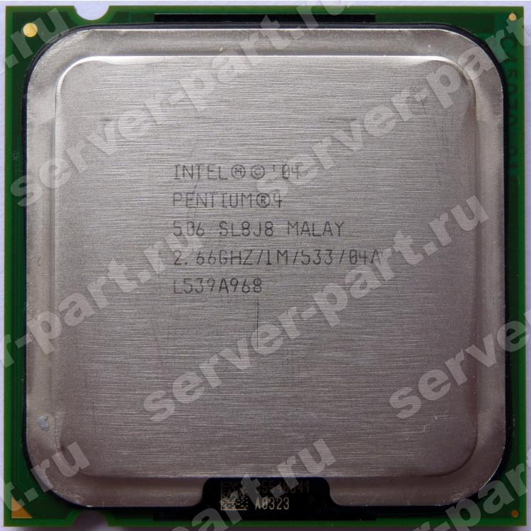 We had already detailed more SKUs in our own leak a few days ago but Igor Wallossek’s leak provides us even more insight into the upcoming CPU family.
Intel 13th Gen Raptor Lake CPU & Raptor Point Z790 PCH’s Official Specifications Leak Out Ahead of Launch
So starting with the specifications, Intel’s 13th Gen Raptor Lake CPUs will utilize the hybrid core design, featuring a mix of Performance-Optimized ‘P’ and Efficiency-Optimized ‘E’ cores. For the new chips, Intel will be using a brand new P-Core known as Raptor Cove which will replace the Golden Cove cores featured on the Alder Lake CPUs. For The E-Core, Intel will retain the existing Gracemont core architecture but it will come with minor improvements.
The enthusiast 125W Intel Raptor Lake-S Desktop SKUs will feature Core i9 models featuring up to 8 Raptor Cove cores and 16 Gracemont cores for a total of 24 cores and 32 threads. Intel’s Core i7 lineup will consist of 16 cores (8+8), and Core i5 models will consist of 14 cores (6+8) and 10 cores (6+4). All Raptor Lake CPUs will come with an increased L3 cache, increased L2 cache per P-Core (2.0 MB), and double the L2 cache per E-core cluster (4.0 MB).
2 of 9
Intel Core i9-13900K 24 Core Raptor Lake CPU Specs
The Intel Core i9-13900K is the flagship Raptor Lake CPU, featuring 24 cores and 32 threads in an 8 P-Core and 16 E-Core configuration. The CPU is configured at a base clock of 3.0 GHz, a single-core boost clock of 5.8 GHz (1-2) cores, and an all-core boost clock of 5.5 GHz (all 8 P-Cores). The CPU features 68 MB of combined cache and a 125W PL1 rating that goes up to 253W. The CPU can also consume up to 350W of power when using the «Unlimited Power Mode» which we detailed here.
- Core i9-13900K 8+16 (24/32) — 3.0 / 5.8 GHz — 66 MB Cache, 125W (PL1) / 253W (PL2)
- Core i9-12900K 8+8 (16/24) — 3.2 / 5.2 GHz — 30 MB Cache, 125W (PL1) / 241W (PL2)
Intel Core i7-13700K 16 Core Raptor Lake CPU Specs
The Intel Core i7-13700K CPU will be the fastest 13th Gen Core i7 chip on offer within the Raptor Lake CPU lineup. The chip features a total of 16 cores and 24 threads. This configuration is made possible with 8 P-Cores based on the Raptor Cove architecture and 8 E-Cores based on the Grace Mont core architecture. The CPU comes with 30 MB of L3 cache and 24 MB of L2 cache for a total combined 54 MB cache. The chip was running at a base clock of 3.4 GHz and a boost clock of 5.40 GHz. The all-core boost is rated at 5.3 GHz for the P-Cores while the E-Cores feature a base clock of 2.5 GHz and a boost clock of 4.2 GHz. The TDP will be retained at 125W (PL1) and 253 (PL2).
- Core i7-13700K 8+8 (16/24) — 3.4 / 5.4 GHz — 54 MB Cache, 125W (PL1) / 253W (PL2)
- Core i7-12700K 8+4 (12/20) — 3.6 / 5.0 GHz, 25 MB Cache, 125W (PL1) / 190W (PL2)
Intel Core i5-13600K 14 Core Raptor Lake CPU Specs
The Intel Core i5-13600K features a total of 14 cores which include 6 P-Cores based on the Raptor Cove and 8 E-Cores based on current Gracemont cores. That’s the same P-Core count as the Intel Core i5-12600K but the E-Core count has been doubled. So we are looking at a 40% core count bump and a 25% thread count bump vs the Alder Lake Core i5-12600K. The CPU comes with 24 MB of L3 and 20 MB of L2 cache for a combined total of 44 MB cache.
Clock speeds are set at 3.5 GHz base, and 5.1 GHz boost, while the E-Cores operate at 2.6 GHz base & 3.9 GHz boost clocks. The i5 will get a slightly toned down PL2 rating of 181W compared to the Core i9 & Core i7 SKUs but that’s still 30 Watts more than the existing 12600K chip.
- Core i5-13600K 6+8 (14/20) — 3.5 / 5.1 GHz — 44 MB Cache, 125W (PL1) /181W (PL2)
- Core i5-12600K 6+4 (10/16) — 3.6 / 4.9 GHz — 20 MB Cache, 125W (PL1) / 150W (PL2)
Intel 13th Gen Raptor Lake-S Desktop CPU Family:
| CPU Name | Silicon Revision / QDF | P-Core Count | E-Core Count | Total Core / Thread | P-Core Base / Boost (Max) | P-Core Boost (All-Core) | E-Core Boost (Max) | Cache (Total L2 + L3) | TDP | MSRP |
|---|---|---|---|---|---|---|---|---|---|---|
| Intel Core i9-13900K | B0 / Q1E1 | 8 | 16 | 24 / 32 | 3. 0 / 5.8 GHz 0 / 5.8 GHz |
5.5 GHz (All-Core) | 4.3 GHz | 68 MB | 125W (PL1) 250W (PL2)? |
TBA |
| Intel Core i9-13900KF | B0 / Q1EX | 8 | 16 | 24 / 32 | 3.0 / 5.8 GHz | 5.5 GHz (All-Core) | 4.3 GHz | 68 MB | 125W (PL1) 250W (PL2)? |
TBA |
| Intel Core i9-13900 | B0 / Q1EJ | 8 | 16 | 24 / 32 | 2.0 / 5.6 GHz | 5.3 GHz (All-Core) | 4.2 GHz | 68 MB | 65W (PL1) ~200W (PL2) |
TBA |
| Intel Core i9-13900F | B0 / Q1ES | 8 | 16 | 24 / 32 | 2.0 / 5.6 GHz | 5.3 GHz (All-Core) | 4.2 GHz | 68 MB | 65W (PL1) ~200W (PL2) |
TBA |
| Intel Core i9-13900T | B0 / ? | 8 | 16 | 24 / 32 | 1.1 / 5.3 GHz | 4.3 GHz (All-Core) | 3.9 GHz | 68 MB | 35W (PL1) 100W (PL2) |
TBA |
| Intel Core i7-13700K | B0 / Q1EN | 8 | 8 | 16 / 24 | 3. 4 / 5.4 GHz 4 / 5.4 GHz |
5.3 GHz (All Core) | 4.2 GHz | 54 MB | 125W (PL1) 228W (PL2)? |
TBA |
| Intel Core i7-13700KF | B0 / Q1ET | 8 | 8 | 16 / 24 | 3.4 / 5.4 GHz | 5.3 GHz (All Core) | 4.2 GHz | 54 MB | 65W (PL1) TBD (PL2) |
TBA |
| Intel Core i7-13700 | B0 / Q1EL | 8 | 8 | 16 / 24 | 2.1 / 5.2 GHz | 5.1 GHz (All-Core) | 4.1 GHz | 54 MB | 65W (PL1) TBD (PL2) |
TBA |
| Intel Core i7-13700F | B0 / Q1EU | 8 | 8 | 16 / 24 | 2.1 / 5.2 GHz | 5.1 GHz (All-Core) | 4.1 GHz | 54 MB | 65W (PL1) TBD (PL2) |
TBA |
| Intel Core i7-13700T | B0 / ? | 8 | 8 | 16 / 24 | 1.4 / 4.9 GHz | 4.2 GHz (All-Core) | 3.6 GHz | 54 MB | 35W (PL1) 100W (PL2) |
TBA |
| Intel Core i5-13600K | B0 / Q1EK | 6 | 8 | 14 / 20 | 3. 5 / 5.2 GHz 5 / 5.2 GHz |
5.1 GHz (All-Core) | TBD | 44 MB | 125W (PL1) 180W (PL2)? |
TBA |
| Intel Core i5-13600KF | B0 / Q1EV | 6 | 8 | 14 / 20 | 3.5 / 5.2 GHz | 5.1 GHz (All-Core) | TBD | 44 MB | 65W (PL1) TBD (PL2) |
TBA |
| Intel Core i5-13600 | C0 / Q1DF | 6 | 8 | 14 / 20 | TBD | TBD | TBD | 44 MB | 65W (PL1) TBD (PL2) |
TBA |
| Intel Core i5-13500 | C0 / Q1DK | 6 | 8 | 14 / 20 | 2.5 / 4.5 GHz | TBD | TBD | 32 MB | 65W (PL1) TBD (PL2) |
TBA |
| Intel Core i5-13400 | C0 / Q1DJ | 6 | 4 | 10 / 16 | 2.5 / 4.6 GHz | 4.1 GHz (All-Core) | 3.3 GHz | 28 MB | 65W (PL1) TBD (PL2) |
TBA |
| Intel Core i3-13100 | H0 / Q1CV | 4 | 0 | 4 / 8 | TBD | TBD | TBD | 12 MB | 65W (PL1) TBD (PL2) |
TBA |
Intel 13th Gen ‘Raptor Lake’ CPUs LGA 1700 Platform
Intel is sticking with its LGA 1700 platform for at least one more CPU lineup and that’s Raptor Lake. Chipzilla confirmed that Raptor Lake CPUs will be compatible with the existing LGA 1700 boards based on the 600-series chipset. But like each generation, motherboard makers will be offering a brand new lineup of motherboards based on the 700-series chipset which will come with higher I/O lanes. In addition to that, Raptor Lake chips will be supporting DDR5-5600 speeds which is a nice bump over the native DDR5-5200 speeds that Alder Lake supports.
The Z790 chipset will offer 20 PCIe Gen 4 & 8 PCIe Gen 3 lanes while the CPUs will feature 16 PCIe Gen 5 and 4 PCIe Gen 4 lanes. We know that the motherboard maker will have a few products which will split the x16 discrete graphics card lanes with an x4 PCIe Gen 5 M.2 slot. Intel won’t have native PCIe Gen 5 M.2 support till 14th Gen Meteor Lake chips.
This offers a nice upgrade path to users who are currently running a mainstream Core i3 or Core i5 CPU and want to upgrade to a higher-end chip. They can simply replace their existing 12th Gen CPU with a higher-end Core i7 or Core i9 SKU which will increase the overall performance of their PC.
Intel Desktop Platform Chipset Comparison
| Chipset Name | Raptor Lake-S (RPL-S) PCH / 700 Series (Z790) | Alder Lake-S (ADL-S) PCH / 600 Series (Z690) | Rocket Lake-S (RKL-S) PCH / 500 Series (Z590) | Comet Lake-S (CML-S) PCH / 400 Series (Z490) | Coffee Lake S (CNL-H) PCH / 300 Series (Z390/h470, B360, Q370, h410) | Coffee Lake S (KBL-R) PCH / Z370 Platform |
|---|---|---|---|---|---|---|
| Process Node | 14nm | 14nm | 14nm | 14nm | 14nm | 22nm |
| Processor | 24,16C,12C,10C,6C,4C (TBD) | 16C,12C,10C,6C,4C (Full corporate/consumer SKU stack at launch) | 8C, 6C (Full corporate/consumer SKU stack at launch) | 10C, 8C, 6C, 4C, 2C (Full corporate/consumer SKU stack at launch) | 8C, 6C, 4C, 2C (Full corporate/consumer SKU stack at launch) | 8C, 6C, 4C (6 Consumer SKUs at Launch) |
| Memory | Up To DDR5-5600 (Native) Up To DDR4-3200 (Native)? |
Up To DDR5-4800 (Native) Up To DDR4-3200 (Native) |
Up To DDR4-3200 (Native) | Up To DDR4-2933 (Native) | Up To DDR4-2666 (Native) | Up To DDR4-2666 (Native) |
| Media, Display & Audio | eDP / 4DDI (DP, HDMI) Display Capabilities | eDP / 4DDI (DP, HDMI) Display Capabilities | DP 1. 2 & HDMI 2.0, HBR3 2 & HDMI 2.0, HBR3HDCP 2.2 (HDMI 2.0a w/LSPCON) 12-bit AV1/HEVC & VP9 10-bit Enc/Dec, HDR, Rec.2020, DX12 Integrated Dual-Core Audio DSP With USB Audio offload SoundWire Digital Audio Interface |
DP 1.2 & HDMI 1.4 HDCP 2.2 (HDMI 2.0a w/LSPCON) HEVC & VP9 10-bit Enc/Dec, HDR, Rec.2020, DX12 Integrated Dual-Core Audio DSP SoundWire Digital Audio Interface |
DP 1.2 & HDMI 1.4 HDCP 2.2 (HDMI 2.0a w/LSPCON) HEVC & VP9 10-bit Enc/Dec, HDR, Rec.2020, DX12 Integrated Dual-Core Audio DSP SoundWire Digital Audio Interface |
DP 1.2 & HDMI 1.4 HDCP 2.2 (HDMI 2.0a w/LSPCON) HEVC & VP9 10-bit Enc/Dec, HDR, Rec.2020, DX12 Integrated Dual-Core Audio DSP |
| I/O & Connectivity | Integrated USB 3.2 Gen 2×2 (20G) Integrated Intel Wireless-AC (Wi-Fi6E/ 7 BT CNVio) with Gig+ Integrated SDXC 4.0 Controller Thunderbolt 4.0 |
Integrated USB 3.2 Gen 2×2 (20G) Integrated Intel Wireless-AC (Wi-Fi6E/ 7 BT CNVio) with Gig+ Integrated SDXC 4.  0 Controller 0 ControllerThunderbolt 4.0 |
Integrated USB 3.2 Gen 2×2 (20G) Integrated Intel Wireless-AC (Wi-Fi6E/ BT CNVi) Integrated SDXC 3.0 Controller Thunderbolt 4.0 (Maple Ridge) |
Integrated USB 3.2 Gen 2 Integrated Intel Wireless-AC (Wi-Fi / BT CNVi) Integrated SDXC 3.0 Controller Thunderbolt 3.0 (Titan Ridge) w/ DP 1.4 |
Integrated USB 3.1 Gen 1 (5 Gbps) Integrated Intel Wireless-AC (Wi-Fi / BT CNVi) Integrated SDXC 3.0 Controller Thunderbolt 3.0 (Titan Ridge) w/ DP 1.4 |
Integrated USB 3.1 Gen 1 (5 Gbps) Thunderbolt 3.0 (Alpine Ridge) |
| Storage | Next-Gen Intel Optane memory PCIe 5.0 (CPU Lanes), 6x SATA 3.0 |
Next-Gen Intel Optane memory PCIe 5.0, 6x SATA 3.0 |
Next-Gen Intel Optane memory PCIe 4.0, 6x SATA 3.0 |
Next-Gen Intel Optane memory PCIe 3.0, 6x SATA 3.0 |
Next Gen Intel Optane memory PCIe 3.0, 6x SATA 3.0 |
Next Gen Intel Optane memory PCIe 3.  0, 6x SATA 3.0 0, 6x SATA 3.0 |
| Max PCH PCIe Lanes | Up To 20 (Gen 4) Up To 8 (Gen 3) |
Up To 12 (Gen 4) Up To 16 (Gen 3) |
Up To 24 (Gen 3) | Up To 24 (Gen 3) | Up To 24 (Gen 3) | Up To 24 (Gen 3) |
| Max CPU PCIe Lanes | TBD | Up To 16 (Gen 5) Up To 4 (Gen 4) |
Up To 20 (Gen 4) | Up To 16 (Gen 3) | Up To 16 (Gen 3) | Up To 16 (Gen 3) |
| Max USB Ports | Up To 5 (USB 3.2 Gen 2×2) Up To 10 (USB 3.2 Gen 2×1) Up To 10 (USB 3.2 Gen 1×1) Up To 14 (USB 2.0) |
Up To 4 (USB 3.2 Gen 2×2) Up To 10 (USB 3.2 Gen 2×1) Up To 10 (USB 3.2 Gen 1×1) Up To 14 (USB 2.0) |
Up To 3 (USB 3.2 Gen 2×2) Up To 10 (USB 3.2 Gen 2×1) Up To 10 (USB 3.2 Gen 1×1) Up To 14 (USB 2.0) |
Up To 10 (USB 3.2) Up To 14 (USB 2.0) |
Up To 10 (USB 3.1) Up To 14 (USB 2.0) |
Up To 10 (USB 3.0) Up To 14 (USB 2.0) |
| Security | N/A | N/A | N/A | Intel SGX 1. 0 0 |
Intel SGX 1.0 | Intel SGX 1.0 |
| Power Management | C10 & S0ix Support for Modern Standby | C10 & S0ix Support for Modern Standby | C10 & S0ix Support for Modern Standby | C10 & S0ix Support for Modern Standby | C10 & S0ix Support for Modern Standby | C8 Support |
| Launch | 2022 | 2021 | 2021 | 2019 | 2018 | 2017 |
Intel 13th Gen Raptor Lake Desktop CPUs Expected Features:
- Up To 24 Cores & 32 Threads
- Brand New Raptor Cove CPU Cores (Higher P-Core IPC)
- Based on 10nm ESF ‘Intel 7’ process node
- Up To 6.0 GHz clock speeds (expected)
- Double The E-Cores on certain variants
- Increased Cache for both P-Cores & E-Cores
- Supported on existing LGA 1700 motherboards
- New Z790, H770, and B760 motherboards
- Up To 28 PCIe Lanes (PCH Gen 4 + Gen 3)
- Up To 28 PCIe Lanes (CPU Gen 5 x16 + Gen 4 x12)
- Dual-Channel DDR5-5600 Memory Support
- 20 PCIe Gen 5 Lanes
- Enhanced Overclocking Features
- 125W PL1 TDP (Flagship SKUs)
- AI PCIe M.
 2 Technology
 - Q4 2022 Launch (October Possibly)
There’s also a new AI M.2 module support that’s supported by Raptor Lake CPUs. As per the latest information we have, there doesn’t seem to be any storage Gen 5 lanes coming directly from the CPU, and motherboard makers would have to split discrete GPU (x16 lanes) with M.2 storage ports to enable Gen 5 SSD support.
Intel Raptor Lake vs AMD Raphael Desktop CPUs Comparison ‘Confirmed’
| CPU Family | AMD Raphael (RPL-X) | Intel Raptor Lake (RPL-S) |
|---|---|---|
| Process Node | TSMC 5nm | Intel 7 |
| Architecture | Zen 4 (Chiplet) | Raptor Cove (P-Core) Gracemont (E-Core) |
| Flagship SKU | Ryzen 9 7950X | Core i9-13900K |
| Cores / Threads | Up To 16/32 | Up To 24/32 |
| Total L3 Cache | 64 MB (+3D V-Cache) | 36 MB |
| Total L2 Cache | 16 MB | 32 MB |
| Total Cache | 80 MB | 68 MB |
| Max Clocks (1T) | 5. 85 GHz 85 GHz |
5.8 GHz |
| Memory Support | DDR5 | DDR5/DDR4 |
| Memory Channels | 2 Channel (2DPC) | 2 Channel (2DPC) |
| Memory Speeds | DDR5-5200 | DDR5-5600 DDR4-3200 |
| Platform Support | 600-Series (X670E/X670/B650/A620) | 600-Series (Z690/H670/B650/H610) 700-Series (Z790/H770/B760) |
| PCIe Gen 5.0 | Both GPU & M.2 (Extreme chipsets only) | Both GPU & M.2 (700-Series only but split) |
| Integrated Graphics | AMD RDNA 2 | Intel Iris Xe |
| Socket | AM5 (LGA 1718) | LGA 1700/1800 |
| TDP (Max) | 170W (TDP) 230W (PPT) |
125W (PL1) 240W+ (PL2) |
| Launch | September 2022 | October 2022 |
News Source: Igor
Future Brings CPU Modules, And The Future Is Now
Modularity is a fun topic for us. There’s something satisfying about seeing a complex system split into parts and these parts made replaceable. We often want some parts of our devices swapped, after all – for repair or upgrade purposes, and often, it’s just fun to scour eBay for laptop parts, equipping your Thinkpad with the combination of parts that fits you best. Having always been fascinated by modularity, I believe that hackers deserve to know what’s been happening on the CPU module front over the past decade.
This “swap your Thinkpad keyboard” video thumbnail captures a modularity-enabled sentiment many can relate to.
We’ve gotten used to swapping components in desktop PCs, given their unparalleled modularity, and it’s big news when someone tries to split a yet-monolithic concept like a phone or a laptop into modules. Sometimes, the CPU itself is put into a module. From the grandiose idea of Project Ara, to Intel’s Compute Card, to Framework laptop’s standardized motherboards, companies have been trying to capitalize on what CPU module standardization can bring them.
There’s some hobbyist-driven and hobbyist-friendly modular standards, too – the kind you can already use to wrangle a powerful layout-demanding CPU and RAM combo and place it on your simple self-designed board. I’d like to tell you about a few notable modular CPU concepts – their ideas, complexities, constraints and stories. As you work on that one ambitious project of yours – you know, the one, – it’s likely you will benefit a lot from such a standard. Or, perhaps, you’ll find it necessary to design the next standard for others to use – after all, we all know there’s never too few standards!
How Is Modularity Still Alive?
We like repairability and upgradeability. Sadly, many consumer-facing gadget-producing companies don’t tend to appreciate these as much as we do – you will see previously omnipresent aspects of modularity, like swappable CPUs or even RAM on laptops, becoming less prevalent with time. Simply put, having us buy new devices is more profitable than letting us upgrade and repair our old devices. Still, there are reasons why modularity lives on – in some important ways, it’s simpler to design modular products. For instance, you don’t have to layout your own board with high-speed CPU and RAM interconnects, able to instead focus on the part that must fit your IO of choice – greatly simplifying design.
An apt demonstration of modular computing upsides being commercially viable, the PC/104 standard has been a staple of industrial computing, in large part because it’s easy to get a replacement motherboard if your old one fails. After all, industrial customers are willing to pay a premium for some degree of modularity, since it means they can get equipment fixed quickly, without losing large amounts of money as their production line is stuck idle. And, when your equipment could use an upgrade due to system requirements rising the way they always do, there’s hardly ever a shortage of PC/104 boards with increased processing power.
Customers don’t have as much of a sway to make modularity in consumer products everpresent. It makes sense from where we stand nowadays, but it’s sad, and doesn’t have to be this way. It also doesn’t help when we have companies like Google and Intel starting attractive modular projects with their own purposes in mind, then screwing a myriad of important aspects up, and ultimately shelving everything. On one hand, bungling products in such a way is a known M.O. of large companies – on the other hand, it’s frustrating to get our hopes up, then have them be represented by a low-effort flop. If you’re not aware of how bad it can get, here’s an example.
The Corporate Way To Get It Wrong
Intel is a giant company manufacturing CPUs, chipsets and all sorts of things that a hobbyist can only dream to one day tinker with. They have both an inordinate amount of resources and a customer base to develop modular solutions, and they’ve been trying to get their own modular, somewhat hobbyist-accessible embedded ideas off the ground, every few years a new one. These ideas have so far been failing, in large part, due to Intel’s own fickle decisions – as many of us somberly familiar with Intel’s Edison and Galileo product lines can attest.
That slot on the left is where you would’ve had inserted your Intel Compute Card – if you had one.
For instance, in 2017, Intel has unveiled the Compute Card concept – a card with CPU, RAM and storage that you could’ve put in your pocket and plugged into anything. Two years later, they’ve shelved the concept. In particular, a politely scathing blog post from NexDock, a company who was trying to develop a Compute Card dock at the time, sheds some light at how rude Intel’s behaviour was. It’s borderline amusing to read about “overly complicated encryption and authentication requirements of Intel Compute Cards”, and nowhere near surprising to read about insufficient support from Intel.
Even though Intel touted NexDock’s efforts as an achievement, it wasn’t enough to warrant proper collaboration and transparency, and NexDock’s ended up spending tons of money and time on something Intel never took seriously. Intel’s latest effort developing CPU+RAM modules is called Intel Compute Element. This one is expressly not for you: it’s for building custom NUCs and other systems with requirements-tailored hardware, reflected by the modules’ price tag. It looks nice in a “what if” way, but by now, we’ve learned to not expect much.
With Enough Resources, We Can Get There Ourselves
Intel presented their Compute Card concept in 2017. In 2016, a surprisingly similar but open-source and hobbyist-friendly project was taking shape. The EOMA68 project invited us to contribute to a future where CPU cards existed – where you could have the CPU, RAM and storage on a small low-power card able to plug into a laptop-shaped housing, game console, a small NUC-like desktop box, or even usable standalone with a HDMI monitor and a powered USB hub. If you’re going somewhere, you can physically take your system out of your desktop enclosure and plug it into a laptop housing, and plug it back when you’ve returned. A lot of the same goals and same form-factor as an Intel’s Compute Card, but none of the corporate backing, it was an daring goal to set, even if you were to get an A20 CPU instead of an x86 system.
Designed by an ambitious engineer set on getting things done, the aim of the EOMA68 project was to never compromise on compatibility while keeping the cards accessible for small-scale design and production – ensuring that after the first compute cards became outdated, building backwards-compatible ones would remain realistic. In a witty move, PCMCIA connectors and housings were used for IO connections – cheap and still widely available. Care was taken to design a pinout which could be compatible with a few different CPU generations going forwards, aiming for upgradability without losing features – and the crowdfunding drive reached its goal as if effortlessly, showing that people believe in what this project stands for.
Getting a batch of EOMA68 cards built proved to be a struggle, however. Manufacturing was an uphill battle, with troubles like connectors going out of stock one after another and replacements causing low yield issues. Time is a cruel mistress and had only stacked extra problems on top of every delay, and the project’s last update has been reassuring but not yet fruitful. However, it’s a journey that one of us ought to have embarked on – even unreleased, this small project achieved things that Intel couldn’t. In addition to that, the author has kept a rich research database, and the development process has been discussed openly on a mailing list – invaluable resources for anyone looking into modular computing.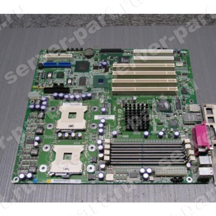
CM4 Form-Factor No Longer Just Theirs
You’re no doubt familiar with Raspberry Pi Compute Modules, but perhaps, not with all the pin-compatible alternatives. When the Pi 4 came out, one of the questions was – how would the next Compute Module look, given the newly added PCIe interface? Most expected a new generation of a SODIMM-mountable module, and what we got was far from that. Once laments about low-pitch alignment-pin-less connectors died down, the promise of PCIe was too much to pass on, and hackers have come out with a wide array of carrier boards and Compute Module-based hacks. There’s almost too many to cover, but we sure try!
Of course, there’s nothing exclusive about a pinout+connector+footprint combination of such a SoM (System-On-Module), and the aforementioned myriad of carrier boards is tempting for any designer wise enough to avoid creating a whole new ecosystem. As a result, you have multiple boards with different – Pine64 SOQuartz, Banana Pi BPI-CM4 and Radxa CM3, to name a few. Each has some benefits over the CM4 – my personal favourites are the eDP-compatible DisplayPort on the SOQuartz and the SATA ports on the CM3, but there’s more to it. Hobbyists are also getting on the CM4-compatible board train with projects like the ULX4M FPGA boards, and there’s a RISC-V CM4-compatible from Antmicro in the works, even.
These modules are not exactly like a computer card that you could swap between your tablet and your desk PC on a daily basis, but it does provide unexpected and pleasant upgradability if you happen to have a device expecting a CM4 baseboard. In times of CM4 module shortages, this is a godsend, too. What’s more, players like TuringPi and MNT Reform have created adapters for their own ecosystems.
Reform The Laptop, CPU Module Ecosystem Comes Free
If you’ve followed projects like Novena, you’ll know that NXP’s i.MX series processors are one of the most openness-friendly ARM CPUs available. Six years after the Novena, the MNT Reform laptop wisely picked an i. MX8 CPU. However, they didn’t want to develop a complex multi-layer baseboard, and went for a DDR-formfactor i.MX8M-hosting SoM from Boundary Devices – making the Reform’s mainboard all that cheaper and simpler to design. The unique part about the Boundary Devices’ SoM – it’s the most open i.MX8M module out there, fit for a laptop that strives to be as open as possible.
To reiterate, there’s nothing exclusive about a pinout + connector + footprint combination – and a DDR formfactor module is just a PCB with a set of gold-plated pads at its edge. You can see where this is going, right? MNT Reform’s team developed some custom SoMs and adapters, compatible with the i.MX8 module’s surface-level connectivity. To date, there’s an adapter for the Pi CM4, consequently compatible with three more aforementioned CPU boards, a NXP LS1028A board with half as many CPU cores but twice as much RAM, and even a Xilinx Kintex-7 FPGA-hosting board with talks about a software-synthesized RISC-V CPU ala Precursor.
What’s more – MNT has recently announced development of the Pocket Reform, a 7″ laptop-shaped companion device. Not to miss such a wonderful opportunity, the MNT Pocket Reform uses this exact module form-factor as its bigger sibling. Now, the MNT lineup became an ecosystem with swappable CPU cards – we didn’t quite expect this to happen, but it’s a pleasant surprise of the kind that we don’t get every day. If you’re working on a yet-unrivaled cyberdeck, you too should consider putting a DDR socket on a PCB and benefitting from everything the MNT ecosystem has to offer.
More To Come, Already Plenty
With each project daring to create a standard – or better yet adhere to an existing one – modular computing becomes more and more of a reality in hacker projects. The CM4 and MNT CPU module standards in particular are both accessible and hacker-friendly. If you wanted to develop a custom highly featureful wearable, or a laptop motherboard swap for that old Thinkpad you grew up with, there’s no better time to start than nowadays. Just like I2C devices have slowly been coalescing on JST-SH connectors, perhaps soon, we’ll be building powerful and sleek computers into whatever we want, at a whim, and our parts drawers will get a new drawer named “CPU modules”.
Headline image: “Back-side of an Intel Celeron LGA775 CPU” by Uwe Hermann
what was shown at the closed presentation — Igromania
The release of Intel Core processors of the 12th generation is on the nose, and on the eve of it, the company Intel held a technical briefing with the press — we were also invited there.
The new 12th Gen Intel Core CPUs feature the new LGA 1700 socket, Intel Z690 chipset, redesigned thermal interface and thermal cover, new TDP standards and process technology, as well as PCIe 5.0, DDR 5, XMP 3.0 , DMI 4.0, advanced overclocking tools, a fundamentally new microarchitecture and a number of other innovations, which we will discuss below.
Processor models and global shortage situation
A total of 60 processors are planned to be built on the Alder Lake architecture, from desktop to mobile. However, only six variants will go on sale first, all with unlocked multipliers: Core i9-12900K , Core i9-12900KF , Core i7-12700K , Core i7-12700KF , and Core i7-12700KF , and Core i7-12700KF Core i5-12600KF . Intel has assured that it will be able to meet customer requests with the proper number of processors, and promised that there will be no supply problems.
LGA 1700 socket
The new LGA 1700 socket is not compatible with all previous Intel processors. Firstly, the number of contacts has increased, so that the old CPUs cannot be installed in it purely physically. Secondly, the processor packaging has now become rectangular instead of square, which, in theory, should impose new requirements on the design of cooling systems. However, representatives of the company could not immediately answer the question of what they will be like — you need to wait for official announcements from manufacturers.
Intel Z690 chipset
Support for Thunderbolt 4.0 , Intel Killer Wi-Fi 6E and VMD (Volume Management Device) technology is promised for the Z690 chipset. The latter is the most interesting, as it came to the user segment directly from server solutions (in other words, borrowed from the Xeon series processors) and allows you to build RAID arrays from NVMe drives without additional hardware controllers. As for the topology of PCIe lanes, we have the following: up to 12 PCIe 4.0 lanes, up to 16 PCIe 3.0 lanes, and up to 16 PCIe 5.0 and 4 PCIe 4.0 lanes go directly from the CPU. The final configuration, as always, will depend on the specific motherboard manufacturer.
Thermal interface
The part of the processors responsible for heat dissipation has undergone serious modifications. The thickness of the thermal interface (solder is used) and the crystal were reduced, while the heat exchanger cover, on the contrary, became thicker.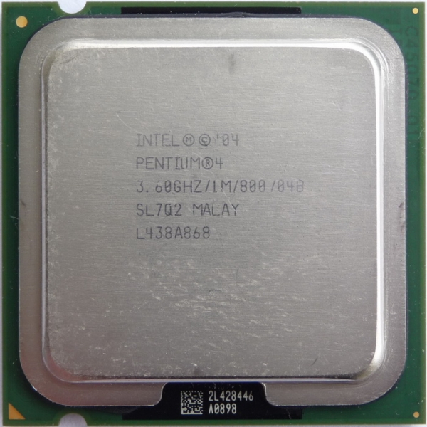 All this should have a positive effect on the overclocking potential of processors and their temperature in normal usage scenarios. Note that at the press conference the word «overclocking» sounded almost in every sentence. Obviously, this time Intel is making a big bet on it, but they did not indicate the exact numbers — they only said that the results will be dictated, as usual, by luck, and therefore the company does not undertake to accurately predict anything. Nevertheless, the conference emphasized more than once that overclocking enthusiasts will be pleased.
PBP instead of the usual TDP
Intel refuses the usual TDP for everyone. It is replaced by PBP (Processor Base Power). This is explained by an attempt to eliminate confusion with an understanding of how much energy a crystal will consume in practice. For example, for all processors with an unlocked multiplier, Intel will now indicate their maximum consumption in PL2 (Power Limit 2) mode. Moreover, all restrictions are now removed from K-processors: they will be able to constantly work in PL2 mode (maximum power) without switching to PL1 low power mode. For example, the technical specification of the flagship Core i9-12900K would look like this: PL1 is equal to PL2, which in turn is equal to 241W. Again, the final limit configuration will depend on Intel partners — say, on motherboard manufacturers. However, for benchmarks and measurements of the maximum performance of new processors, Intel recommends removing all possible restrictions in the BIOS.
Process
The workflow in the 12th generation of Core processors is called «7». This is a marketing name that is not related to nanometers and reflects what solutions from, for example, TSMC competes with one or another Intel processor. The publication Gamers Nexus talked about this in more detail, but if we restrict ourselves to a simple explanation, then the 10-nm crystals manufactured by Intel, , in their opinion and in practice, compete with TSMC’s 7-nm products, which means they should be called » 7″. So now 10nm is «7», and the upcoming 7nm is «4». The technical specification, however, as before, will indicate the real numbers, that is, 10 nm for the 12th generation of Core processors.
Memory subsystem Alder Lake
Alder Lake, among other things, brings a lot of changes regarding the processor memory subsystem. The cache memory will finally be increased to 30 MB in the third level for the top Core i9-12900K. Well, as for the second level, it will be divided between P and E-cores (read below about what it is): 1.25 MB for each P-core and 2 MB for a cluster of four E-cores . In addition, we are expecting a transition to DDR5, but for those who are not ready to change the memory yet, there is good news: DDR4 will also be supported. The market will most likely not see hybrid boards that support both memory standards at once (at least in large numbers) — these will be either DDR5 or DDR4 models. It will be possible to overclock modules, as in the case of the 11th generation of Intel Core processors, on Z, H and B chipsets. True, according to Tom’s Hardware, H and B chipsets will only support DDR4.
At the same time, technology XMP (Xtreme Memory Profile) will also receive an update. Instead of two factory profiles under the meaningless numbers “1” and “2”, there will now be three — each can be named as you like for convenience, plus there will be an option to save two additional user profiles.
Well, the last innovation is Intel Dynamic Memory Boost Technology or, in Russian, dynamic boost of the memory subsystem. That is, at peak load, it will operate at maximum frequency, and during downtime it will fall. Why this is needed in practice, no one answered, but we assume that in order not to torment DDR modules with excessive voltage in 24/7 mode. Another question is what frequency reduction algorithms will be used and whether the timings will change dynamically. And how to test all this for stability is also not clear yet. Well, we are waiting for the release.
Alder Lake microarchitecture
We got to the most interesting part: microarchitecture. There are changes in a wagon and a small trolley — let’s say right away that on paper the processors look very interesting. Intel itself calls the microarchitecture hybrid, and it is based on a combination of productive P-cores (Performance Cores) and energy-efficient E-cores (Efficient Cores). Energy-efficient cores are typed in blocks of four and do not support virtual multithreading, while for P-cores technology Hyper-Threading is enabled.
For a better understanding, let’s analyze the topology using the Core i9-12900K with 24 threads as an example. It has 8 productive cores on one chip, each of which has one virtual thread (that’s already 16 threads) plus 8 energy-efficient cores. All other Intel Alder Lake CPUs will be built according to the same scheme. For example, the i7-12700K will have 8 P-cores and 4 E-cores, while the i5-12600K will have 6 P-cores and 4 E-cores. At the same time, productive cores, according to Intel, will receive up to 19% increase in IPC (the number of executable instructions per processor cycle) compared to the 11th generation cores, and the energy-efficient cores are comparable in terms of their processing power to the cores of the Intel Core i7-6700K — the first CPU with the Skylake microarchitecture. When asked why they decided to use a hybrid CPU structure in the desktop segment, although it would be wiser to leave such an architecture only for mobile solutions, the company replied: «The future belongs to hybrid technologies.»
Well, an interesting approach, but it raised a lot of questions, the main one being “How, in fact, will all this work?” And here we come to perhaps the most interesting innovation: the Intel Thread Director technologies. This can be translated into Russian as “flow manager”, and the essence of his work is the constant collection of extremely voluminous telemetry. It includes data on the load of the cores, their temperature, the type of instructions executed on the cores, the type of task (priority or background) — and all this happens all the time. Further, this telemetry is sent for processing to the task scheduler Windows , and the catch here is this: only the scheduler Windows 11 is fully optimized to work with the 12th generation of Intel Core, while all previous versions of OS Microsoft meet the needs of Thread Director only partially. Simply put, they simply do not have the necessary tools to process all the telemetry data, which means that the new Alder Lake processors running any system other than Windows 11 will no longer work as efficiently.
The question of what numbers could be used to express the difference in performance of new processors in Windows 11 and 10 environments could not be answered. But one thing turned out for sure: while there are problems in the operation of the technology, not all software can cope with it. In particular, Intel noted that there are problems with Denuvo (game hacking protection technology), but assured that it is already in dialogue with developers and soon all the difficulties will come to naught. Plus, the company added that the Thread Director API is completely open and transparent, so there should not be any difficulties with writing software code for it. As for other operating systems — for example, based on kernel Linux , then full support for Intel Thread Director is promised in the very near future.
Acceleration
As we noted earlier, overclocking during the press conference was given increased attention. They promised high results and said that the processors had a huge frequency potential. For overclocking, as usual, there is everything you need: unlocked P and E-core multipliers, cache memory, DDR memory, integrated graphics, and overclocking on the bus is also provided. In addition, it will be possible to set your own multiplier and enable Hyper Threading separately for each core, configure AVX offsets, control the dynamic boost of the memory subsystem, shift the maximum temperature threshold, overclock PEG and DMI, and experiment with CPU PLL.
For those who do not want to overclock in the BIOS of the motherboard, there is an updated utility Intel Extreme Tuning Utility . In it, you can do almost everything the same, and to save time, the overclocking function “in one click of the mouse” is implemented.
Terminals
Well, on paper, Intel came out with very interesting processors with a truly revolutionary microarchitecture. There are a lot of innovations, the platform is literally built from scratch. Promises of increased performance and crazy overclocking also sound optimistic, but all this remains to be tested in practice, so stay tuned for our publications. Very soon we will share the results of our testing of new CPUs and give them our own verdict.
|
Socket (colloquial — socket) of the central processor is a socket located on the computer motherboard to which the central processor is connected. The processor, before it is installed in the motherboard, must match its socket. It is very easy to figure out what a processor socket is, if you remember that the latter is a microcircuit, only of a relatively large size. Sometimes forums ask which socket to choose. In fact, you should first select a processor, and already under it — a board with the appropriate socket. However, one important point must be taken into account. Intel is «famous» for the fact that often each new generation of processors involves the use of a new socket. This can lead to the fact that a recently purchased computer based on the processor of this company will be difficult to upgrade in a few years due to the incompatibility of the installed microprocessor and the new ones offered on the market. AMD has a more loyal attitude towards customers: changing sockets is slower, and backward compatibility is usually maintained.
Share: Leave your comment!
Add a comment
|
What is a socket.
The main sockets of processors AMD and Intel
The concept of a socket is, perhaps, a kind of passive characteristic of the processor, but at the same time this term is one of the key ones when completing a system. In this article of the «Processor Specifications» series, we will deal with the concept of a socket and consider the more or less popular processor sockets of the two main CPU manufacturers — AMD and Intel.
Socket. What and how?
Simply put, a socket is a slot (socket) on the motherboard where the processor is installed. But when we say “processor socket”, we mean by this both the socket on the motherboard and the support of this socket by certain processor lines. The socket is needed precisely so that you can easily replace a failed processor or upgrade the system with a more powerful processor.
At the physical level, sockets differ in the number of pins, the type of pins, the distance of fasteners for CPU coolers, and many other little things that make almost all sockets incompatible. Also, there are technological differences: the presence of various additional controllers, higher performance parameters, support for integrated graphics in the processor, etc.
As mentioned above, socket selection is an important part of system assembly. If a processor is selected that is oriented to a different socket than in the motherboard, then the system will not work, if at all the processor will fit into an incompatible socket. It is better not to carry out such experiments with incompatible sockets, since you can damage the contacts on the processor or socket, which will most likely lead to failure of the components. Therefore, when buying a motherboard and processor, first choose a processor, and then look for a motherboard with a compatible socket for it. The list of supported processors can be found on the official website of the motherboard manufacturer in order to make sure that a particular model is compatible.
Well, now, we will look at the most popular processor sockets from amd and intel, omitting the outdated versions like the 370th sockets for Pentium III and the like.
Intel sockets
The dynamics of socket updates for Intel processors is an order of magnitude higher than for the same sockets of new AMD processors. As part of its penultimate series of processors, as many as three new sockets have appeared, and they are completely incompatible.
All this is both good and bad at the same time. The good thing is that with frequent socket updates and releases for each (even) part of the processor line, we can see an increase in performance and more specific sharpening for a specific model. But the fat minus is that it is quite difficult to upgrade, when each new series of processors goes to a new socket, you have to change not only the processor, but also the motherboard.
Now let’s look at a few specific sockets from Intel:
Socket It should be noted that this socket was rather a marketing ploy to shake up the market and increase prices (at first) for processors that were positioned under this socket. Still, performance improvements could be seen. Now, processors for this socket have fallen in price, which cannot be said about motherboards with LGA 2011, they remain many times more expensive than similar motherboards for the same LGA 1155, which we will consider below.
Socket , just for different versions.
Socket 1155 turned out to be the most popular, and most systems are now built on it. For powerful systems and server solutions on board with Corei7 and Xeon, Socket 1366 was developed.
Socket ( socket LGA 775) — these sockets are already obsolete, although they still live in many systems, they were positioned under several lines at once, such as Core 2 Duo, Core 2 Quad, Celeron and others.
AMD sockets
AMD’s policy is more conservative in this regard. Several sockets are compatible due to series with «+». For example, Socket AM2 is compatible with AM2+, which gives more upgrade opportunities, but at the same time, it’s a bit of an unpleasant treadmill, which is not acceptable for the IT industry.
Some examples of AMD sockets:
SOKKET (socket AM 3 and AM 3+) — I can say, they can say that they could say, pre -consults. FX, Phenom II, Athlon II processors. The socket for the most powerful Bulldozer (FX) among the AMD camp, which did not live up to expectations, but having fallen in price has become a more interesting application in terms of good performance for a low price. Sockets AM3 and AM3+ are now the most popular, they are equipped with most of both cheap and more expensive systems. That is, we can safely state the practicality of these sockets.
Socket Also, fully compatible. Today it can be considered a little outdated, although a lot of systems built on the basis of these sockets are still actively working.
Socket (socket FM 1 and FM 2)0166 AMD Fusion , which feature very powerful integrated graphics. This socket and compatible processors should be guided by those who do not want to spend money on a discrete video card and will be content with integrated graphics.
Here we have examined, in a rather detailed form, the concept of a socket and the main sockets of intel and amd processors. I recommend that you read other articles on the site, which describe other characteristics of processors.
A little more than detailed addition for specific sockets is described in the comments to the article, I also recommend that you read it.
Intel LGA 1700 socket — release date, processors, motherboards
Intel LGA 1700 socket
Intel LGA 1700 is a new socket for Intel 12 generation Alder Lake S processors for home PCs. They will be used on motherboards with the new socket. The release date of the new socket is the 2nd half of 2021.
These powerful and still in development processors will succeed the 11th generation of Intel Rocket Lake. The 12th generation Intel CPUs are likely to be based on the 10nm process technology.
Check out the new Intel processors on Yandex.Market!
- Intel has confirmed that their next generation Alder Lake S desktop processors will run on the new LGA 1700 socket. In general, Intel makes a big breakthrough in performance with 12 generation processors.
Intel LGA 1200 VS Intel LGA 1700
According to rumors from people who work directly with Intel, the twelfth generation of Alder Lake S CPUs running on the new Intel LGA 1700 socket will be brought to stores in 2022.
- This means that Intel won’t be supporting motherboards on the Z-490 for very long. During this time, the new Comet Lake S and Rocket Lake S processors will dominate the market. The new Intel LGA 1700 socket will support as many as 3 generations of processors! In terms of dimensions, the LGA 1700 will be larger than the LGA 1200 and LGA 1151, its actual dimensions are 45mm x 37.5mm.
LGA-1700 Socket cooler
This change in physical size and form factor will cause some problems with coolers.
Gamers with decent fans, for example, will also have to change them, which will cost them a pretty penny. But gamers are not one of those who save on components ….))
New motherboards based on the Z-490 chipset and LGA-1200 socket, for example ASRock Z-490 Phantom Gaming 4SR, may lose their relevance in just a year and a half.
- The new socket form factor will directly affect the physical size of the processor, giving the manufacturer new opportunities for architectural changes.
Nearly half of the available cores on the architecture work to achieve maximum power, while the other half are focused on operating at the lowest power level. By the way, this is a very smart decision.
It is also worth mentioning that processors and motherboards using the Intel LGA 1700 socket are expected to support PCI-e 5.0, but not immediately, but after some time, a little later.
But these CPUs will have very high heat dissipation, and they are more suitable for some more difficult tasks.
In addition, despite the fact that they are positioned as desktop PCs, Intel 12th generation processors are fully compatible with DDR-5 RAM.
The
11th generation Intel Rocket Lake serves as a transitional processor and the last to be made on the outdated 14nm process technology.
- Simply put, Rocket Lake has a 14nm backport of a future generation core architecture that many say is a cross between Sunny Cove and Willow Cove with an XE graphics solution.
Alder Lake
Alder Lake-s
CPUs Other future Alder Lake processors will use next generation Golden Cove cores. By the way, not only the new architecture itself is important, but also the selection of design and implementation of these same cores.
Intel will implement its Golden Cove and Gracemont cores on the same platform, and will adopt next generation XE graphics with improvements.
Rocket Lake CPUs will be used in conjunction with an LGA-1200 socket, but Alder-Lake will require a completely different motherboard — on an LGA-1700 socket.
- Specifically, Intel did not deny this information, providing information about the support of Alder Lake S on the Intel LGA 1700. The material was published on the official page.
The LGA 1700 uses a completely different layout. In fact, this is a large rectangular niche measuring 45 mm x 37.5 mm.
In addition to the physical difference in form factor, LGA 1700 socket motherboards will be the first to support DDR-5 RAM!
- New socket 9 motherboards0166 Intel LGA 1700 should work fine with DDR5-4800 and DDR5-4000 RAM.
I don’t need to explain that this is just a huge breakthrough in technology and in particular in the speeds of DDR4 RAM — 2933 MHz!
Intel 12-gen Alder Lake S Stones will go on sale sometime in early 2022. Everything suggests that these processors will become quite successful commercially, manufactured on a 10-nanometer process technology and equipped with a special hybrid technology.
- In addition to the architecture and implementation, these CPUs will also be equipped with an improved version of the XE graphics processor (video card).
According to rumors, Intel is trying to increase the power of Alder Lake S processors with heat dissipation to 150 watts.
This Intel processor with a high heat dissipation profile can easily compete with the 16-core AMD Ryzen-9 3950 X CPU in the high performance desktop segment! Read also about the most powerful processor AMD Ryzen Threadripper PRO 3995 WX!
LGA 1700 socket motherboards
ASUS ROG Maximus XIV
Planned support for the next generation ASUS Z690 and ROG Maximus XIV motherboards based on socket LGA 1700, which will support Intel Alder Lake processors.
ASUS has yet to announce its line of Z690-based chipsets, but they are expected to be introduced in the second half of 2021.
- Support for ASUS Z690 and ROG Maximus XIV motherboards has been added just a few weeks after the company added support for Intel 13th Gen Raptor Lake-S desktop processors.
We know that both Intel Alder Lake-S (12th generation) and Raptor Lake-S (13th generation) desktop processors will be compatible with LGA 1700 motherboards.
Intel Alder Lake-S chips will initially be supported by the 600 series chipset family, while the PCH 700 series update is planned for the Raptor Lake processor line.
MAIN
Sockets by years. AMD processor sockets
Processor socket
— connector, a place on the computer where the processor is inserted. The processor, before it is installed in the motherboard, must match its socket. It’s like a socket and a contact plug — needless to say, a euro plug will not work with a simple Soviet socket.Usually in computer stores, next to each processor, you can see a plate that lists its main characteristics. So the processor socket is almost the most important characteristic, and it is on it that you first of all need to pay attention when buying a new processor. Because it may happen that the processor does not fit the computer motherboard precisely because of the socket.
Just imagine — you came to a computer store, chose a processor there, paid money for it and came home satisfied, start installing it — but it DOES NOT SUIT! You drop everything, run back to the store, hoping to return this processor back and thereby correct the situation, you resort, and they tell you — «this is not a warranty case, you should have looked more carefully when you bought it.
» Well, okay, it was a small lyrical digression. And now let’s talk specifically about these same sockets.
The whole variety of sockets can be divided into two large groups:
- Intel processor sockets.
- AMD processor sockets.
Below are pictures of sockets from both processor companies.
In this photo you can see that the «legs» of the pins stick out of the socket on the motherboard.
And in this photo, on the contrary, you can see the recesses for these contacts, and they themselves are located directly on the processor.
Let’s see how the sockets physically differ so dramatically from each other
:- Number of contacts
- The type of these same contacts
- Distance of fastenings for CPU coolers
- The actual size of the socket itself
Number of contacts — there can be 400, 500, 1000 and even more. How to find out? The socket marking already contains all the information.
For example, the Intel Pentium 4 processor has an LGA 775 socket. So 775 is just the number of contacts, and LGA means that the processor does not have contact legs (pins), they are in the motherboard socket.
Type of contacts — everything is clear here, either «pins» or contacts without pins. There is no other way, as they say.
Now about the distances between the mounts for CPU coolers. The fact is that these distances are different for each socket, and special attention should also be paid to this. Although there are “do-it-yourself” methods, when a cooler from one socket is attached to another socket with the help of skillful hands and something else. sockets from each other in terms of technology. A sockets are technologically different from each other
:- Various optional
- The presence or absence of support for processor-integrated graphics (processor graphics core)
- Higher performance options
controllers available
What else does the processor socket affect?
In addition to what is already written here, processor socket
also affects the size of the processor itself.Generally speaking, if I try to put it very briefly — the processor socket affects which processor will be installed in it. Everything else (for example, what will be written here further in the text) depends on the processor, but we all know that the processor and the socket are two inseparable concepts. Therefore, all those parameters that depend on the processor (or are affected by the processor) also depend on the socket of this processor.
Perhaps I will give a few more points that the processor (or its socket) can influence, in other words, the processor or its socket affect:
- Type of supported RAM
- Bus frequency FSB
- Indirectly (chipset mostly) to PCI-e slot version
- Per version (also indirectly)
What is a socket for?
The fact is that the manufacturers of modern motherboards purposefully left us the opportunity to change various devices, including the processor. This is where such a concept as a socket appears, because from the point of view of manufacturers, it would be quite possible to solder the processor directly to the mat.
board, and in terms of reliability it is more appropriate. But this was done, frankly, on purpose — that is, on purpose. for possible system upgrades. In other words, we wanted to replace the processor with another one — we pulled it out of the socket and inserted the one we needed, of course, with the amendment that it should have the same socket as the old processor. In truth, it is for the possible modernization of computer hardware that the vast majority of slots and connectors exist that are only on the motherboard.
Now let’s talk about socket support for various processors. Below is a table with popular (at the time of publication of the material) sockets and their corresponding processors:
Socket (socket) Processor LGA 775 (Socket T), manufactured in 2004 Intel Pentium 4
Pentium 4 Extreme Edition
Intel Celeron D
Pentium D
Pentium Extreme Edition
Pentium Dual-Core
Core 2 Duo
Core 2 Extreme
Core 2 Quad
Xeon (for servers)LGA 1366 (Socket B) Started in 2008 Intel Core i7 (9xx)
Intel Celeron P1053LGA 1156 (Socket H), start of production — 2009 Intel Core i7 (8xx)
Intel Core i5 (7xx, 6xx)
Intel Core i3 (5xx)
Intel Pentium G69x0
Intel Celeron G1101
Intel Xeon X,L (34xx)LGA 1155 (Socket h3), production year — 2011 Sandy Bridge
and Intel Ivy Bridge
LGA 1150 (Socket h4), planned release year — (2013-2014) Intel Haswell
and Intel Broadwell
Socket 939, year of manufacture — no data Athlon 64
Athlon 64 FX
Athlon 64 X2Socket AM2, manufactured in 2006 Athlon 64 (not all)
Athlon 64 X2 (not all)
Athlon X2
Athlon 64 FX-62
Opteron 12xx
Sempron (some)
Sempron X2
Phenom (limited support)Socket AM2+, manufactured in 2007 Athlon X2
Athlon II
Opteron 13xx
Phenom
Phenom IISocket AM3, manufactured in 2009 Phenom II (except X4 920 and 940)
Athlon II
Sempron 140
Opteron 138xSocket AM3+, manufactured in 2011 AMD FX-Series(AMD FX-4100 AMD FX-6100 and AMD FX-8120 AMD FX-8150) Socket FM1, year of production — 2011 All processors with AMD Fusion microarchitecture
Socket FM2, year of production — 2012 All processors with Bulldozer microarchitecture
And in conclusion, a small recommendation for those who are going to buy a new processor: before buying, always check the compatibility of the motherboard socket and processor.
For example, if the motherboard has an LGA775 socket — take processors that are made specifically for this socket, no other processors will work.
Intel processor sockets
- Socket 1 — Intel 80486 and compatible processors from other manufacturers
- Socket 2 — Intel 80486 and compatible processors from other manufacturers
- Socket 3 — Intel 80486 and compatible processors from other manufacturers
- Socket 4 — Intel Pentium (early versions)
- Socket 5 — Intel Pentium, AMD K5, IDT WinChip C6, WinChip 2
- Socket 6 — 80486DX4
- Socket 7 — Intel Pentium, Pentium MMX, AMD K6
- Super Socket 7 — AMD K6-2, AMD K6-III; Rise mP6
- Socket 8 — Intel Pentium Pro
- Socket 370 — Pentium III (800 MHz — 1.4 GHz), Celeron Cyrix III; VIA C3
- Socket 423 — Intel Pentium 4 and Celeron processors (based on the Willamette core)
- Socket 478 — Intel Pentium 4 and Celeron processors (based on the Northwood, Prescott and Willamette cores)
- Socket 479 — Intel Pentium M and Celeron M (based on Banias and Dothan cores)
- Socket 480 — Intel Pentium M processors (based on the Yonah core)
- Socket 603/604 — Intel Xeon processors based on the Northwood and Willamette Pentium 4 cores
- Socket 771 — Intel Xeon DP processors for server motherboards (Dempsey,
Woodcrest, Harpertown, Clovertown) - Socket T/LGA 775 (Land Grid Array) — Intel Pentium 4 and Celeron processors (based on Northwood and Prescott cores)
- Socket 1156 — Intel Core i5 and Core i7 9 processors0550
- Socket 1155 — Intel processors based on the Intel Sandy Bridge Core i5 and
core i7.Designed to replace Socket 1156. Sockets 1155 and 1156 are not compatible.
Also known as Socket h3. - Socket 1366 — Intel Core i7 and Intel Xeon processors. Also known as Socket B
- Socket 2011 — multi-core Intel Core i7 processors. Designed to replace
Socket 1366 and also known as Socket R. 4-channel memory mode is used.
There is no integrated graphics. - Socket 1150 — released in 2013 to replace Socket 1155 for Intel processors
Haswell (and its successor Broadwell). Not compatible with Socket 1155.
Also known as Socket h4. Processors under Socket 1150 — with 2 or 4 cores.
One of the major innovations in the Haswell microarchitecture is
this is a new graphics core with support for DirectX 11.1, OpenCL 1.2 and OpenGL 4.0. - Socket 1151 — released to replace Socket 1150 for Skylake architecture Intel processors. Supports DDR4 memory,
Intel Rapid Storage Technology, Intel Clear Video Technology, and Intel Wireless Display Technology. - Socket 1151.
v2 — Released Q4 2017 to support Intel 8th generation Coffee Lake processors. 8th generation processors are not compatible with socket LGA 1151 of 7th generation processors.
These processors require a motherboard with a 300-series chipset and an updated version of LGA 1151.v2.
The 7th generation Skylake and Kaby Lake processors do not work with LGA 1151.v2. This fact was refuted by enthusiasts from China, who modified the BIOS microcode and launched 7th generation processors on motherboards with a 300 series chipset.
and 8th generation processors — on motherboards with a 100 series chipset. - LGA 2066 (Socket R4) — socket for Skylake-X and Kaby Lake-X architecture processors without an integrated graphics core. Designed
as a replacement for the LGA 2011/2011-3 socket (Socket R/R3) for high-performance desktop PCs based on the Basin Falls platform (X299 chipset). - LGA 3647 (Socket P) replacement for LGA 2011-1/2011-3 (Socket R2/R3) in Skylake-EX (Xeon Purley) based server platforms.
AMD processor sockets
- Socket 462 (aka Socket A) — AMD Athlon, Athlon XP, Sempron and Duron 9 processor versions0550
- Socket 754 — low-end AMD Athlon 64 processors and Sempron processors with single-channel memory only support
- Socket 939 — AMD Athlon 64 and AMD Athlon FX processors with dual-channel memory support
- Socket 940 — AMD Opteron processors and early AMD Athlon FX (differs from 939 in one «leg», which is used to control the correctness of data read from memory (ECC).
- Socket AM2 (AM2+)
cores Windsor and Brisbane), Athlon 64 FX, Athlon 64 and Sempron. - Socket AM3 (AM3+) — Athlon II X2, Athlon II X4, Phenom II X3 processors,
Phenom II X4, Sempron 140.
Socket-AM3+ — updated version of Socket-AM3.
Socket-AM3+ is fully compatible with AM3 processors.
Socket-AM3 motherboard will require BIOS update when working with AM3+ processors
Socket-AM3+ supports power saving mode. Socket-AM3+ case is black, Socket-AM3 case is white. - Socket FM1 —
Socket FM1 — for processors with AMD Fusion microarchitecture.
Represents a ZIF connector c 905 contacts,
which is designed for the installation of processors in PGA-type cases. - Socket FM2 — for Piledriver architecture processors. It was introduced in 2012, just one year after Socket FM1. Although Socket FM2 is
development of the FM1 socket, it is not backwards compatible with it. Structurally, it is a ZIF connector
c 904 contacts, which is designed for the installation of processors in PGA-type packages. - Socket AM4 — for Zen architecture processors. Introduced in 2016. Supports DDR4, USB 3.1, PCI-E 3.0.
Structurally, it is a connector with 1331 pins, which is designed for installing processors in PGA-type cases. - Socket TR4 — AKA SP3r2 for consumer motherboards and Socket SP3 for EPYC servers. Represents a 4094-pin socket for Threadripper processors. Physical dimensions of both sockets
are identical. It is highly optimized for heat dissipation and requires the use of new cooling systems, or at least new mounts for existing ones. - Socket 370
— the most common socket for Intel processors. It is with him that the era of Intel processors separation into inexpensive Celeron solutions with a cropped cache and Pentium — more expensive full versions of the company’s product begins.The connector was installed on motherboards with a system bus from 60 to 133 MHz. The socket is made in the form of a square plastic movable box; when installing a processor with 370 pins, a special plastic lever pressed the processor legs to the connector pins. Supported processors Intel Celeron Coppermine, Intel Celeron Tualatin, Intel Celeron Mendocino, Intel Pentium Tualatin, Intel Pentium Coppermine. The speed characteristics of the installed processors are from 300 to 1400 MHz. Supported third-party processors. Produced since 1999 years.
- Socket 423
— the first socket for Pentium 4 processors. It had a 423-pin grid of legs, it was used on personal computer motherboards. It lasted less than a year, due to the impossibility of the processor to further increase in frequency, the processor could not pass the frequency of 2 GHz. Replaced by Socket 478. Launched in 2000. - Socket 478
— released after the competitor’s (AMD) Socket A, as previous processors could not raise the bar to 2 GHz, and AMD took the lead in the processor manufacturing market.The connector supports Intel solutions — Intel Pentium 4, Intel Celeron, Celeron D, Intel Pentium 4 Extreme Edition. Speed characteristics from 1400 MHz to 3.4 GHz. Produced since 2000.
- Socket 754
was developed specifically for the Athlon 64 model processor.The release of new processor sockets was associated with the need to replace the Athlon XP processor line, which was based on Socket A. The first AMD K8 platform processors were installed in Socket 754 processor sockets measuring 4 by 4 centimeters. This need was dictated by the fact that Athlon 64 processors had a new bus and integrated memory controllers. The voltage output by this socket was 1.5 volts. Of course, 754 became an intermediate stage in the development of Athlon 64. The high cost and initial scarcity of these processors did not make this platform very popular. And by the time when the availability and cost of components had just returned to normal, AMD presented the release of a new socket — Socket 939. By the way, it was he who helped make the Athlon 64 a popular and really affordable processor.
- Socket 775
or Socket T — the first socket for Intel processors without sockets, made in a square form factor with protruding contacts.The processor was installed on the protruding contacts, the pressure plate was lowered, and with the help of a lever it was pressed against the contacts. It is still used in many personal computers. Designed to work with almost all fourth-generation Intel processors — Pentium 4, Pentium 4 Extreme Edition, Celeron D, Pentium Dual-Core, Pentium D, Core 2 Quad, Core 2 Duo and Xeon series processors. Produced since 2004. The speed characteristics of the installed processors are from 1400 MHz to 3800 MHz.
- Socket 939
, which contains 939 contacts of extremely small diameter, due to which they are quite soft. This is a «simplified» version of the previous Socket 940, commonly used in high performance computers and servers. The absence of one hole in the socket made it impossible to install more expensive processors into it. This connector was considered very successful for its time, as it combined good features, dual-channel memory access and low cost, both the socket itself and the controller in computer motherboards. These connectors were used for computers with conventional DDR memory. Immediately after the transition to DDR2 memory, they became obsolete and gave way to AM2 connectors. The next step is the invention of the new DDR3 memory and the new AM2+ and AM3 sockets for the following quad-core processors from AMD. - socket AM2
(Socket M2) developed by AMD for some types of desktop processors (Athlon-LE, Athlon 64, Athlon 64 FX, Athlon 64 X2, Sempron-LE and Sempron, Phenom X4 and Phenom X3, Opteron). It came to replace Socket 9 connectors39 and 754. Although Socket M2 has 940 pins, this socket is not compatible with Socket 940 because the older version of Socket 940 cannot support dual-channel DDR2 memory. The first processors supporting Socket AM2 were single-core Orleans (or 64th Athlon) and Manila (Sempron), some dual-core Windsor (for example, Athlon 64, X2 FX) and Brisbane (AthlonX2 and Athlon 64X2). In addition, Socket AM2 includes Socket F for servers and a Socket S1 variant for various mobile computers. Socket AM2+ i
is absolutely identical in appearance to the previous one, the difference lies only in the support of processors with Agena and Toliman cores. - LGA 1156 socket
– Made with 1156 protruding contacts. Produced since 2009. Designed for modern Intel processors for personal computers. Speed characteristics from 2.1 GHz and above.
- LGA 1155 socket
or Socket H2 — designed to replace the LGA 1156 socket. Supports the most modern Sandy Bridge processor and the future Ivy Bridge.The connector is made in 1155 pin version. Produced since 2011. Speed characteristics up to 20 GB / s.
- Socket
R (LGA2011) — Core i7 and Xeon with integrated quad-channel memory controller and two QuickPath connections. Replacement Socket B (LGA1366) - Socket FM1
is AMD’s platform for Llano processors and looks like a tempting proposition for those who love integrated systems. - Socket h4 or LGA 1150 — Processor socket for Intel microarchitecture Haswell (and its successor Broadwell), released in 2013. LGA 1150 is designed as a replacement for LGA 1155 (Socket h3).
Made using LGA (Land Grid Array) technology. It is a connector with spring-loaded or soft contacts, to which the processor is pressed using a special holder with a grip and a lever. The LGA 1150 socket has been officially confirmed to be used with the Intel Q85, Q87, H87, Z87, B85 chipsets. Mounting holes for cooling systems on sockets 1150/1155/1156 are completely identical, which means full all-round compatibility and identical order of mounting cooling systems for these sockets.
- Socket B2 (LGA1356) — Core i7 and Xeon with integrated tri-channel memory controller and QuickPath connections. Replacement Socket B (LGA1366)
- FM2 connector —
Processor socket for AMD APUs with Piledriver core architecture: Trinity and Komodo, as well as canceled Sepang and Terramar (MCM — multi-chip module). Structurally, it is a ZIF — connector with 904 pins, which is designed for installing processors in PGA-type cases.
The FM2 connector was introduced in 2012, just one year after the FM1 connector.Although the FM2 socket is an evolution of the FM1 socket, it is not backwards compatible with it. Trinity processors have up to 4 cores, Komodo and Sepang server chips up to 10, and Terramar up to 20 cores.
- LGA 1151 socket
— An Intel processor socket that supports Skylake architecture processors.The LGA 1151 is designed as a replacement for the LGA 1150 socket (also known as Socket h4). The LGA 1151 has 1151 spring-loaded pins to make contact with the CPU pads. According to rumors and leaked Intel promotional documentation, motherboards with this connector will support DDR4 memory type. All Skylake architecture chipsets support Intel Rapid Storage Technology, Intel Clear Video Technology, and Intel Wireless Display Technology (if supported by the processor). Most motherboards support various video outputs (VGA, DVI or — depending on the model).
- LGA 2066 (Socket R4) is an Intel processor socket that supports Skylake-X and Kaby Lake-X architecture processors without an integrated graphics core.
Designed as a replacement for the LGA 2011/2011-3 socket (Socket R/R3) for high-end desktop PCs based on the Basin Falls platform (X299 chipset), while the LGA 3647 (Socket P) will replace the LGA 2011-1/2011- 3 (Socket R2/R3) in Skylake-EX (Xeon «Purley») based server platforms.
- AM4 (PGA or µOPGA1331) is a socket by AMD for microprocessors with Zen microarchitecture (Ryzen brand) and later. The connector is of the PGA (pin grid array) type and has 1331 pins. It will be the company’s first socket to support the DDR4 memory standard and will be a single socket for both high-performance processors without an integrated video core (currently using Socket AM3+) and low-cost processors and APUs (previously used various sockets of the AM / FM series).
- Socket TR4 (Socket Ryzen Threadripper 4, also Socket SP3r2) is a socket type from AMD for the Ryzen Threadripper family of microprocessors, introduced on August 10, 2017. Physically very close to the AMD Socket SP3 server socket, however, it is incompatible with it.
Socket TR4 became the first LGA-type connector for consumer products (previously LGA was used in the server segment, and processors for home computers were produced in an FC-PGA package). It uses a complex multi-stage process of mounting a processor into a socket using special retaining frames: an internal one, fixed with latches to the cover of the microcircuit case, and an external one, fixed with screws to the socket. Journalists note the very large physical size of the connector and socket, calling it the largest format for consumer processors. Because of its size, it requires specialized cooling systems that can draw up to 180 watts. The socket supports HEDT (High-End Desktop) segment processors with 8-16 cores and provides the ability to connect RAM via 4 DDR4 SDRAM channels. The socket runs 64 Gen 3 PCIexpress lanes (4 are used for the chipset), multiple 3.1 lanes, and SATA
AMD sockets will be considered in this article. At the moment, the company’s model range has four processor sockets. Each of them is aimed at a certain part of the computer systems market. It is about them that will be discussed in the future.
List of processor sockets
Today there are the following current sockets:
For office computers, the most optimal is AM1. The key advantages of this computing platform are low cost and an acceptable performance level for solving the most simple tasks.
The FM2+ processor socket boasts a higher level of performance. The main scope of its application is multimedia stations and entry-level.
Even more powerful is the AM3/AM3+ platform, which is already ideal for building mid-range gaming computers.
Announced at the beginning of March belongs to the premium class solutions. Its processors allow solving the most complex tasks.
AM1 socket — the ideal solution for office systems
In April 2014, the AM1 platform debuted.
Its second name is PGA-771. These processors have 771 pins, 4 processing cores, an integrated video adapter, a low clock speed and 2 levels of cache memory. The performance of this platform is enough to solve the most simple tasks, which include office suites or browsing websites. The younger CPU models belong to the Septron line, and the older ones belong to the AMD Athlon. Socket AM1 allows you to use the entire line of these processors.
FM2+ Processor Socket
Some AMD sockets allow you to install processor solutions with an integrated performance video subsystem. These include FM1, FM2 and the current FM2+. The second designation of the latter is PGA904. This platform is suitable for building an entry-level gaming system or an advanced station.
AM3 and AM3+ performance platforms
Until recently, one of the most productive processor sockets from AMD was AM3/AM3+. The first wave of these solutions debuted in 2009year and was called AM3. The Septron and Athlon II series chips belonged to it.
The flagship processor in this case was the second generation AMD Phenom.
The AM3+ socket debuted in 2011 with the FX-XXXX series processors. The speed of these CPUs was lower than that of similar Intel products, but sufficient to solve a wide range of tasks. An additional advantage of this platform is the lower cost of computing systems based on it. These processor sockets are compatible with each other. Unlike the previously considered platforms, in this case a video card was not integrated into the processor chip. But higher performance was provided by a cache memory system of 3 levels.
The younger AM1 and FM2+ chips boast only two levels of fast memory. This family of processors is great for creating mid-range gaming systems. Also, based on them, you can implement an entry-level server or a graphical station.
The most recent socket AM4
In December 2016, AMD introduced an updated computer platform, which received the designation AM4, or PGA1331.
It was supposed to bring together all the previously considered AMD sockets: both the simplest PCs and high-performance computing systems should be created on its basis. In this case, the north and south bridges of the system logic set are included in the chip.
This die layout improves the performance of the processor unit and reduces the cost of manufacturing motherboards. The chips for this socket are from the Rizen line. The younger ones have an index of 3 and include 4 cores and 8 logical threads. Medium CPU models come with an index of 5 and have 6 cores and 12 threads. The flagship line of chips has an index of 7, is physically equipped with 8 cores that can process code in 12 threads.
Results
In this article, the main AMD sockets were considered. Whatever it was, and the main one is AM4. It is this processor socket that will replace all the others in the foreseeable future, and both entry-level personal computers and high-performance computing systems will be assembled on its basis.
All other solutions will disappear from store shelves as inventory sells out.
Socket (colloquial — socket) of the central processor is a connector located on the computer motherboard to which the central one is connected. The processor, before it is installed in the motherboard, must match its socket. It is very easy to figure out what a processor socket is, if you remember that the latter is a microcircuit, only of a relatively large size. The socket is located on the motherboard, outwardly it looks like a low rectangular structure with many holes, the number of which corresponds to the legs of the processor. A mechanical latch of a special design is used to securely fix the inserted microcircuit in the socket. Note that Intel, unlike AMD, has recently been using a different principle for connecting the processor and the board.
Sometimes forums ask which socket to choose. In fact, you should first select a processor, and already under it — a board with the appropriate socket.
However, one important point must be taken into account. Intel is «famous» for the fact that often each new generation of processors involves the use of a new socket. This can lead to the fact that a recently purchased computer based on the processor of this company will be difficult to upgrade in a few years due to the incompatibility of the installed microprocessor and the new ones offered on the market. AMD has a more loyal attitude towards customers: changing sockets is slower, and backward compatibility is usually maintained. Although, times are changing.
Type
Purpose
Number of contacts
Year of manufacture
PIN DIP 8086/8088, 65C02 40 1970 CLCC Intel 80186, 80286, 80386 68 1980 PLCC Intel 80186, 80286, 80386 68 1980 Socket 80386 Intel 386 132 1980 Socket 486 / Socket 0 Intel 486 168 1980 Motorola 68030 Motorola 68030, 68LC030 128 1987 Socket 1 Intel 486 169 1989 Type
Purpose
Number of contacts
Year of manufacture
Socket 2 Intel 486 238 1989 Motorola 68040 68040 179 1990 Socket 3 Intel 486, 5×86 237 1991 Socket 4 Pentium 273 1993 Type
Purpose
Number of contacts
Year of manufacture
Socket 5 Intel 486 238 1994 Socket 463 NexGen Nx586 463 1994 Motorola 68060 68060, 68l0C60 206 1994 Socket 7 Pentium, AMD K5, K6 321 1995(Intel), 1998(AMD) Type
Purpose
Number of contacts
Year of manufacture
Socket 499 DEC EV5 21164 499 1995 Socket 8 Pentium/Pentium 2 387 1955 Socket 587 DEC EV5 21164A 587 1996 Mini Cartridge Pentium 2 240 1997 MMC-1 Mobile Module Connector Pentium 2, Celeron 280 1997 Apple G3/G4/G5 G3/G4/G5 300 1997 MMC-2 Mobile Module Connector Pentium 2. 3, Celeron
400 1998 Type
Purpose
Number of contacts
Year of manufacture
G3 / G4 ZIF Power PC G3 G4 288 1996 Socket 370 Pentium 3, Celeron, Cyrix, Via C3 370 1999 Socket A / Socket 462 AMD Athlon, Duron, MP, Sempron 462 2000 Socket 423 Pentium 4 423 2000 Type
Purpose
Number of contacts
Year of manufacture
Socket 478 / Socket N / Socket P Intel 486 238 1994 Socket 495 / MicroPGA 2 Mobile Celeron / Pentium 3 495 2000 PAC 418 Intel Itanium 418 2001 Socket 603 Intel Xeon 603 2001 PAC 611 / Socket 700 / mPGA 700 Intel Itanium 2, HP8800, 8900 611 2002 Type
Purpose
Number of contacts
Year of manufacture
Socket 604 / S1 Intel 486 238 2002 Socket 754 Athlon 64, Sempron, Turion 64 754 2003 Socket 940 Opteron 2, Athon 64FX 940 2003 Socket 479 / mPGA479M Pentium M, Celeron M, Via C7-M 479 2003 Socket 478v2 / mPGA478C Pentium4, Pentium Mobile, Celeron, Core 478 2003 Type
Purpose
Number of contacts
Year of manufacture
Socket 939 Intel 486 939 2004 LGA 775 / Socket T Pentium4, Celeron D, Core 2, Xeon 775 2004 Socket 563 / Socket A / Compact Mobile Athon XP-M 563 2004 Socket M / mPGA478MT Celeron, Core, Core 2 478 2006 LGA771 / Socket J Xeon 771 2006 Socket A. This socket is known as Socket 462 and is a socket for processors from Athlon Thunderbird models to Athlon XP/MP 3200+ models, as well as AMD processors such as Sempron and Duron. The design is made in the form of a ZIF socket with 453 working contacts (9 contacts are blocked, but despite this, the number 462 is used in the name). The system bus for Sempron, XP Athlon has a frequency of 133 MHz, 166 MHz and 200 MHz. The mass of coolers for Socket A, recommended by AMD, should not exceed 300 grams.
The use of heavier coolers (coolers) can lead to mechanical damage and even lead to failure of the processor power system. Processors with a frequency of 600 MHz (for example, Duron) and up to 2300 MHz (meaning the Athlon XP 3400+, which was never sold) are supported.
Type
Purpose
Number of contacts
Year of manufacture
Socket S1 Athon Mobile, Sempron, Turion 64/X2 638 2006 Socket AM2 / AM2+ Athon 64/FX/FX2, Sempron, Phenom 940 2007 Socket F / Socket L / Socket 1207FX Athon 64FX, Opteron 1207 2006 Socket / LGA 1366 Xeon 1366 2008 rPGA988A / Socket Q1 Core i3/i5/i7, Pentium, Celeron 988 2009 LGA 1366 socket
– Completed in 1366 contact form, produced since 2008. Supports Intel — Core i7 9 series processorsxx, Xeon series 35xx to 56xx, Celeron P1053.FROM
speed characteristics from 1600 MHz to 3500 MHz. Core i7 and Xeon (35xx, 36xx, 55xx, 56xx series) with integrated 3-channel memory controller and QuickPath connection. Replacement for Socket T and Socket J (2008)Type
Purpose
Number of contacts
Year of manufacture
Socket AM3 AMD Phenom, athlon, Sempron 941 2009 Socket G / 989 / rPGA G1/G2 989 2009 Socket h2 / LGA1156/a/b/n Core i3/i5/i7, Pentium, Celeron, Xeon 1156 2009 Socket G34 / LGA 1944 Opteron 6000 series 1944 2010 Socket C32 Opteron 4000 series 1207 2010 Type
Purpose
Number of contacts
Year of manufacture
LGA 1248 Intel Itanium 9300/9600 1248 2010 Socket LS / LGA 1567 Intel Xeon 6500/7500 1567 2010 Socket h3 / LGA 1155 Intel Sandy Bridge, Ivy Bridge 1155 2011 LGA 2011 / Socket R Intel Core i7 Xeon 2011 2011 Socket G2 / rPGA988B Intel Core i3/i5/i7 988 2011 Type
Purpose
Number of contacts
Year of manufacture
Socket FM1 AMD Liano/Athlon3 905 2011 Socket AM3 AMD Phenom/Athlon/Semron 941 2011 Socket AM3+ Amd Phenom 2 Athlon 2 / Opteron 3000 942 2011 Socket G2 / rPGA989B Intel Core i3/i5/i7, Celeron 989 2011 Socket FS1 AMD Liano/Trinity/Richard 722 2011 Socket AM3 is a desktop processor socket that is a further development of Socket AM2+. This connector has support for DDR3 memory, as well as faster HyperTransport bus speeds. The first processors to use this socket were Phenom II X3 710-20 and Phenom II X4 model 805, 910 and 810.
Socket AM3+ (Socket 942) is a modification of Socket AM3 designed for processors codenamed «Zambezi» (microarchitecture — Bulldozer). Some motherboards with socket AM3 will be able to update BIOS and use processors with socket AM3+. But when using AM3+ processors on motherboards with AM3, it may not be possible to get data from the temperature sensor on the processor. Also, the power saving mode may not work due to the lack of support for fast core voltage switching in Socket AM3. Socket AM3+ on motherboards is black while AM3 is white. The diameter of pin holes in processors with Socket AM3 + exceeds the diameter of pin holes in processors with Socket AM3 — 0.51 mm against the previous 0.
45 mm.
Type
Purpose
Number of contacts
Year of manufacture
LGA 1356 / Socket B2 Intel Sandy Bridge 1356 2012 Socket FM2 AMD Trinity/athlon X2/X4 904 2012 Socket h4 / LGA 1150 Intel Haswell/Broadwell 1150 2013 Socket G3 / rPGA 946B / 947 Intel Haswell/Broadwell 947 2013 Socket FM2 / FM2b AMD Kaveri/Godvari 906 2014 Type
Purpose
Number of contacts
Year of manufacture
LGA 2011-3 / LGA 2011 v3 Intel Haswell, haswell-EP 2011 2014 Socket AM1 / FS1b AMD Athlon/Semron 721 2014 LGA 2011-3 Intel Haswell/Xeon/haswell-EP/ivy Bridge EX 2083 2014 LGA 1151 / Socket h5 Intel Skylake 1151 2015 Type
Purpose
Number of contacts
Year of manufacture
LGA 2066 Socket R4 Intel Skylake-X/Kabylake-X i3/i5/i7 2066 2017 Socket TR4 AMD Ryzen Threadripper 4094 2017 Socket AM4 AMD Ryzen 3/5/7 1331 2017 Leave your comment!
ASUS P8H67-M PRO Intel® H67 LGA 1155 (Socket h3) Motherboards (P8H67-M PRO B3)
This is a demo of a seamless insert of an Icecat LIVE product data-sheet in your website.
Imagine that this responsive data-sheet is included in the product page of your webshop. How to integrate Icecat LIVE JavaScript.
Place this product description on your website
Icecat LIVE: JS for ASUS P8H67-M PRO B3
Icecat Live DOC
CSV data for ASUS P8H67-M PRO B3
CSV DOC
Download images
Icecat extensions
Download free Open Icecat catalog
Download Icecat taxonomy for «Motherboards»
Icecat PDFMore>>>
Short summary description ASUS P8H67-M PRO Intel® H67 LGA 1155 (Socket h3):
This short summary of the ASUS P8H67-M PRO Intel® H67 LGA 1155 (Socket h3) data-sheet is auto-generated and uses the product title and the first six key specs.
ASUS P8H67-M PRO, Intel, LGA 1155 (Socket h3), Intel® Core™ i3, Intel® Core™ i5, Intel® Core™ i7, 5 GT/s, 32 GB, Dual-channel
Long summary description ASUS P8H67-M PRO Intel® H67 LGA 1155 (Socket h3):
This is an auto-generated long summary of ASUS P8H67-M PRO Intel® H67 LGA 1155 (Socket h3) based on the first three specs of the first five spec groups.
ASUS P8H67-M PRO. Processor manufacturer: Intel, Processor socket: LGA 1155 (Socket h3), Compatible processor series: Intel® Core™ i3, Intel® Core™ i5, Intel® Core™ i7. Maximum internal memory: 32 GB, Memory channels: Dual-channel, Supported memory frequencies: 1066.1333 MHz. RAID levels: 0, 1, 5, 10. Parallel processing technology supported: Quad-GPU CrossFireX, Graphics adapter memory capacity: 1748 MB.
Ethernet interface type: Gigabit Ethernet, LAN controller: Realtek RTL8111E, Network performance: 10/100/1000 Mbit/s
Place this product description on your website
Icecat LIVE: JS for ASUS P8H67-M PRO B3
Icecat Live DOC
CSV data for ASUS P8H67-M PRO B3
CSV DOC
Download images
Icecat extensions
Download free Open Icecat catalog
Download Icecat taxonomy for «Motherboards»
Report an error
EN Access to this product is restricted. Please contact your account manager at Icecat.
Specifications
Specifications
Processor
Processor manufacturer
*Intel
Processor socket
*LGA 1155 (Socket h3)
Compatible processor series
*Intel® Core™ i3, Intel® Core™ i5, Intel® Core™ i7
System bus baud rate
5 GT/s
Memory
Number of memory slots
*4
Memory channels
Dual-channel
without error correction
Supported memory frequencies
1066.
1333 MHz
Maximum internal memory
*32 GB
Supported memory modules
8GB
Data storage controllers
Levels RAID
0, 5, 10
Graphic adapter
Graphic adapter volume
1748 MB
Support for parallel processing technology
*Quad-GPU CrossFireX
Integrated graphics
Internal ports
USB 2.0 connectors
*5
Number of SATA III connectors
*4
Number of connectors SATA
6
S/PDIF
Explanatory Exploration Actual Panel
ATX power connector
Device for fan 9000
Central processor fan connector
Number of chassis fan connectors
1
EPS power connector (8-pin)
Number of COM connectors
1
TPM connector
Number of USB ports 90
*4
Number of USB 3.
2 Gen 1 (3.1 Gen 1) Type-A ports
*2
Number of Ethernet LAN ports ( RJ-45)
*1
Number of PS/2 ports
1
Number of VGA (D-Sub) ports
*1
Number of HDMI ports
*1
Number of DVI-D ports
*1
S/PDIF output port
Digital optical audio exit
6
Network
Ethernet Interface
Gigabit Ethernet
Controller LAN
Realtek RTL811111111111111111111111111111111111111111111111111111111111111111111111111IE
10/100/1000 MBIT/S 9000 2 $ 9000 9000 fees
*Intel® H67
Audio chip
Realtek ALC892
Accessories for
*PC
Power Supply Type
ATX
Expansion Slots
PCI Express x16 Slots
2
PCI Slots
PCI Express Slot Version 90 2 0007
2.
- This means that Intel won’t be supporting motherboards on the Z-490 for very long. During this time, the new Comet Lake S and Rocket Lake S processors will dominate the market. The new Intel LGA 1700 socket will support as many as 3 generations of processors! In terms of dimensions, the LGA 1700 will be larger than the LGA 1200 and LGA 1151, its actual dimensions are 45mm x 37.5mm.