List of Intel Pentium M Microprocessors
The Pentium M brand refers to single-core 32-bit mobile CPUs codenamed Banias and Dothan, and targeted at the consumer market of mobile computers.
1.1. Pentium M
«Banias» (130 nm)
- All models support: MMX, SSE, SSE2, Enhanced Intel SpeedStep Technology (EIST)
- Die size: 83 mm²
| Pentium M 1.3 | | 1.3 GHz | 1 MiB | 400 MT/s | 13× | 0.956–1.388 V | | | | March 12, 2003 | | |-
| Pentium M 1.4 | | 1.4 GHz | 1 MiB | 400 MT/s | 14× | 0.956–1.388 V | | | | March 12, 2003 | | |-
| Pentium M 1.5 | | 1.5 GHz | 1 MiB | 400 MT/s | 15× | 0.956–1.484 V | | | | March 12, 2003 | | |-
| Pentium M 705 | | 1.5 GHz | 1 MiB | 400 MT/s | 15× | 0.956–1.484 V | | | | May 10, 2004 | | |-
| Pentium M 1.6 | | 1.6 GHz | 1 MiB | 400 MT/s | 16× | 0.956–1.484 V | | | | March 12, 2003 | | |-
| Pentium M 1.7 | | 1.7 GHz | 1 MiB | 400 MT/s | 17× | 0. 956–1.484 V | | | | June 2, 2003 | | |-
| Pentium M 1.8[1][2] | | 1.8 GHz | 1 MiB | 400 MT/s | 18× | 0.956–1.484 V | | | | May 10, 2004 | | |-
| Pentium M LV 1.1 | | 1.1 GHz | 1 MiB | 400 MT/s | 11× | 0.956–1.18 V | | | | March 12, 2003 | | $272 |-
| Pentium M LV 1.2 | | 1.2 GHz | 1 MiB | 400 MT/s | 12× | 0.956–1.18 V | | | | June 2, 2003 | | |-
| Pentium M LV 718 | | 1.3 GHz | 1 MiB | 400 MT/s | 13× | 0.956–1.18 V | | | | April 6, 2004 | | |-
| Pentium M ULV 900 | | 900 MHz | 1 MiB | 400 MT/s | 9× | 0.844–1.004 V | | | | March 12, 2003 | | |-
| Pentium M ULV 1.0 | | 1 GHz | 1 MiB | 400 MT/s | 10× | 0.844–1.004 V | | | | June 2, 2003 | | |-
| Pentium M ULV 713 | | 1.1 GHz | 1 MiB | 400 MT/s | 11× | 0.844–1.004 V | | | | April 6, 2004 | | |-
|}
«Dothan» (90 nm)
- All models support: MMX, SSE, SSE2, Enhanced Intel SpeedStep Technology (EIST)
- PAE, XD bit (an NX bit implementation): supported by C0 stepping
- Die size: 87 mm²
- Steppings: B0, B1, C0
- C1 stepping Pentium M’s are fabbed on a 65 nm process with an actual C0 stepping[3][4]
| Pentium M 710[5][6] | | 1.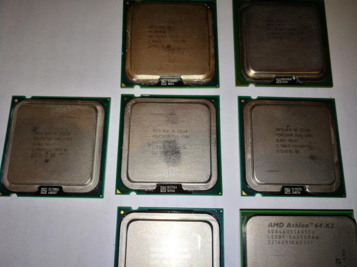 4 GHz | 2 MiB | 400 MT/s | 14× | 0.988–1.34 V | | | | June 23, 2004 | | OEM |-
| Pentium M 715 | | 1.5 GHz | 2 MiB | 400 MT/s | 15× | 0.988–1.34 V | | | | June 23, 2004 | | $209 |-
| Pentium M 715A[7][8] | | 1.5 GHz | 2 MiB | 400 MT/s | 15× | 0.988–1.34 V | | | | May 10, 2004 | | OEM |-
| Pentium M 725 | | 1.6 GHz | 2 MiB | 400 MT/s | 16× | 0.988–1.34 V | | | | June 23, 2004 | | $241 |-
| Pentium M 725A[9][10] | | 1.6 GHz | 2 MiB | 400 MT/s | 16× | 0.988–1.34 V | | | | July 2005 | | OEM |-
| Pentium M 730 | | 1.6 GHz | 2 MiB | 533 MT/s | 12× | 1.26–1.356 V | | | | January 19, 2005 | | $209 |-
| Pentium M 735 | | 1.7 GHz | 2 MiB | 400 MT/s | 17× | 0.988–1.34 V | | | | May 10, 2004 | | $294 |-
| Pentium M 735A[11][12] | | 1.7 GHz | 2 MiB | 400 MT/s | 17× | 0.988–1.34 V | | | | May 10, 2004 | | OEM |-
| Pentium M 740 | | 1. 73 GHz | 2 MiB | 533 MT/s | 13× | 1.26–1.356 V | | | | January 19, 2005 | | $241 |-
| Pentium M 745 | | 1.8 GHz | 2 MiB | 400 MT/s | 18× | 1.276–1.34 V | | | | May 10, 2004 | | $423 |-
| Pentium M 745A | | 1.8 GHz | 2 MiB | 400 MT/s | 18× | 1.276–1.34 V | | | | May 10, 2004 | | OEM |-
| Pentium M 750 | | 1.87 GHz | 2 MiB | 533 MT/s | 14× | 1.26–1.356 V | | | | January 19, 2005 | | $294 |-
| Pentium M 755 | | 2 GHz | 2 MiB | 400 MT/s | 20× | 0.988–1.34 V | | | | May 10, 2004 | | $637 |-
| Pentium M 760 | | 2 GHz | 2 MiB | 533 MT/s | 15× | 1.26–1.356 V | | | | January 19, 2005 | | $423 |-
| Pentium M 765 | | 2.1 GHz | 2 MiB | 400 MT/s | 21× | 0.988–1.356 V | | | | October 20, 2004 | | $637 |-
| Pentium M 770 | | 2.13 GHz | 2 MiB | 533 MT/s | 16× | 1.26–1.372 V | | | | January 19, 2005 | | $637 |-
| Pentium M 780 | | 2.27 GHz | 2 MiB | 533 MT/s | 17× | 1.26–1.404 V | | | | July 25, 2005 | | $637 |-
| Pentium M LV 738 | | 1. 4 GHz | 2 MiB | 400 MT/s | 14× | 0.988–1.116 V | | | | July 20, 2004 | | $284 |-
| Pentium M LV 758 | | 1.5 GHz | 2 MiB | 400 MT/s | 15× | 0.988–1.116 V | | | | January 19, 2005 | | $284 |-
| Pentium M LV 778 | | 1.6 GHz | 2 MiB | 400 MT/s | 16× | 0.988–1.116 V | | | | January 19, 2005 | | $284 |-
| Pentium M ULV 723 | | 1 GHz | 2 MiB | 400 MT/s | 10× | 0.812–0.94 V | | | | July 20, 2004 | | $241 |-
| Pentium M ULV 733 | | 1.1 GHz | 2 MiB | 400 MT/s | 11× | 0.812–0.956 V | | | | July 20, 2004 | | $262 |-
| Pentium M ULV 733J | | 1.1 GHz | 2 MiB | 400 MT/s | 11× | 0.812–0.956 V | | | | July 2005 | | $262 |-
| Pentium M ULV 753 | | 1.2 GHz | 2 MiB | 400 MT/s | 12× | 0.812–0.956 V | | | | January 19, 2005 | | $262 |-
| Pentium M ULV 773 | | 1.3 GHz | 2 MiB | 400 MT/s | 13× | 0.812–0.956 V | | | | January 19, 2005 | | $262 |-
|}
Intel processor brand names-Xeon,Core,Pentium,Celeron—-Pentium — baihuahua
This article is about the Pentium brand.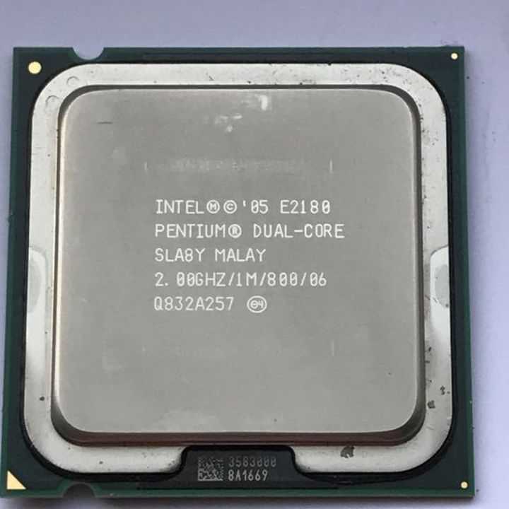 For the original Pentium CPU, see P5 (microarchitecture).
| This article needs additional citations for verification. Please help improve this article by adding citations to reliable sources. Unsourced material may be challenged and removed. (August 2007) |
Pentium is a brand used for a series of x86-compatible microprocessors produced by Intel. In its most current form, a Pentium processor is a consumer-level product that Intel rates as «two stars»,[1] meaning that it is above the low-endAtom and Celeron products but below the faster Core i3, i5 and i7 lines as well as the high-end Xeon processors.
March 22, 1993 – December 2005 logo
December 2005–9 logo
The name Pentium is originally derived from the Greek word pente (πέντε), meaning «five» (as the original Pentium processors used Intel’s fifth-generation microarchitecture, the P5), and the Latin ending -ium. The current Pentium processors only share the name but are in fact based on the same processor chips that are used in the Intel Core but are typically used with a lower clock frequency, a partially disabled L3 cache and some of the advanced features such ashyper-threading and virtualization disabled.
Contents
[hide]
- 1 Overview
- 2 History
- 3 Pentium-branded processors
- 3.1 P5 microarchitecture based
- 3.1.1 Pentium
- 3.2 P6 microarchitecture based
- 3.2.1 Pentium Pro
- 3.2.2 Pentium II
- 3.2.3 Pentium III
- 3.3 Netburst microarchitecture based
- 3.3.1 Pentium 4
- 3.3.2 Pentium D
- 3.4 Pentium M microarchitecture based
- 3.4.1 Pentium M
- 3.4.2 Pentium Dual-Core
- 3.5 Core microarchitecture based
- 3.5.1 Pentium Dual-Core
- 3.5.2 Pentium (2009)
- 3.6 Nehalem microarchitecture based
- 3.
 7 Sandy Bridge microarchitecture based
 - 3.8 Ivy Bridge microarchitecture based
- 3.1 P5 microarchitecture based
- 4 Pentium compatible Intel processors
- 5 See also
- 6 References
Overview[edit]
See also: List of Intel Pentium microprocessors
During development Intel generally identifies processors with codenames, such as Prescott, Willamette, Coppermine,Katmai, Klamath or Deschutes. These usually become widely known,[2] even after the processors are given official names on launch.
| Brand | Microarchitecture | Desktop | Laptop | Server |
|---|---|---|---|---|
| Pentium Pentium OverDrive |
P5 | P5 (0.8 µm) P54C (0.6 µm) P54CS (0.35 µm) |
||
| Pentium MMX Pentium OverDrive MMX |
P55C (0.35 µm) Tillamook (0.25 µm) |
|||
| Pentium Pro | P6 | P6 (0.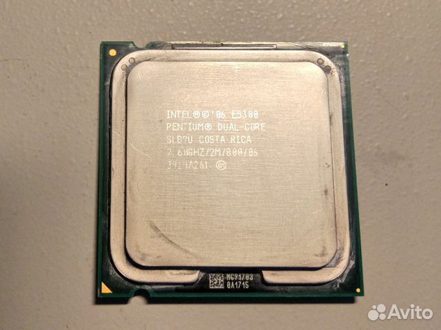 5 µm) 5 µm)P6 (0.35 µm) |
||
| Pentium II Pentium II Xeon Pentium II OverDrive Mobile Pentium II |
Klamath (0.35 µm) Deschutes (0.25 µm) |
Tonga (0.25 µm) Dixon (0.25 µm) |
Drake (0.25 µm) | |
| Pentium III Pentium III Xeon Mobile Pentium III Pentium III M |
Katmai (0.25 µm) Coppermine (180 nm) Tualatin (130 nm) |
Coppermine (180 nm) Tualatin(130 nm) |
Tanner (0.25 µm) Cascades (180 nm) |
|
| Pentium 4 Pentium 4 Extreme Edition |
NetBurst | Willamette (180 nm) Northwood (130 nm) Gallatin (130 nm) Prescott-2M (90 nm) Prescott (90 nm) Cedar Mill (65 nm) |
Northwood (130 nm) Prescott (90 nm) |
Rebranded as Xeon |
| Pentium D Pentium Extreme Edition |
Smithfield (90 nm) Presler (65 nm) |
|||
| Pentium M | P6 based | Banias (90 nm) Dothan (65 nm) |
||
| Pentium Dual-Core | Yonah (65 nm) | |||
| Core | Allendale (65 nm) Wolfdale-3M (45 nm) |
Merom-2M (65 nm) | ||
| Pentium | Wolfdale-3M (45 nm) | Penryn-3M (45 nm) | ||
| Nehalem | Clarkdale (32 nm) | Arrandale (32 nm) | ||
| Sandy Bridge | Sandy Bridge (32 nm) | |||
| Ivy Bridge | Ivy Bridge (22 nm) | |||
| Haswell | Haswell (22 nm) | |||
History[edit]
The original Pentium branded CPUs were expected to be named 586 or i586, to follow the naming convention of previous generations (286, i386, i486). However, as the company wanted to prevent their competitors from branding their processors with similar names (as AMD had done with their Am486), Intel attempted to file atrademark on the name in the United States, only to be denied because a series of numbers was not considered distinct.[3]
Following Intel’s previous series of 8086, 80186, 80286, 80386, and 80486 microprocessors, the company’s first P5-based microprocessor was released as theoriginal Intel Pentium on March 22, 1993. Marketing firm Lexicon Branding was hired to coin a name for the new processor. The suffix -ium was chosen as it could connote a fundamental ingredient of a computer, like a chemical element,[4] while the prefix pent- could refer to the fifth generation of x86.[3]
Due to its success, the Pentium brand would continue through several generations of high-end processors. In 2006, the name briefly disappeared from Intel’sroadmaps,[5][6] only to re-emerge in 2007. [7]
[7]
In 1998, Intel introduced the Celeron[8] brand for low-priced microprocessors. With the 2006 introduction of the Intel Core brand as the company’s new flagship line of processors, the Pentium series was to be discontinued. However, due to a demand for mid-range dual-core processors, the Pentium brand was re-purposed to be Intel’s mid-range processor series, in between the Celeron and Core series, continuing with the Pentium Dual-Core line.[9][10][11]
In 2009, the «Dual-Core» suffix was dropped, and new x86 microprocessors started carrying the plain Pentium name again.
Pentium-branded processors[edit]
P5 microarchitecture based[edit]
The original Pentium and Pentium MMX processors were the superscalar follow-on to the 80486 processor and were marketed from 1993 to 1999. Some versions of these were available as Pentium OverDrive that would fit into older CPU sockets.
Pentium[edit]
Main article: List of Intel Pentium microprocessors
| Core | Process | Frequency | L1 Cache | FSB | Socket | Release date |
|---|---|---|---|---|---|---|
| P5 | 0.8 µm | 60–66 MHz | 16 KB | 60–66 MHz | Socket 4 | March 1993 |
| P54C | 0.6 µm | 75–120 MHz | 16 KB | 50–66 MHz | Socket 5 | October 1994 |
| P54CS | 0.35 µm | 133–200 MHz | 16 KB | 60–66 MHz | Socket 7 | June 1995 |
| P55C | 0.35 µm | 120–233 MHz | 32 KB | 60–66 MHz | Socket 7 | January 1997[12] |
| Tillamook | 0.25 µm | 166–300 MHz | 32 KB | 66 MHz | Socket 7 | August 1997 |
P6 microarchitecture based[edit]
In parallel with the P5 microarchitecture, Intel developed the P6 microarchitecture and started marketing it as the Pentium Pro for the high-end market in 1995. It introduced out-of-order execution and an integrated second level cache on dual-chip processor package. The second P6 generation replaced the original P5 with the Pentium II and rebranded the high-end version as Pentium II Xeon. It was followed by a third version called the Pentium III and Pentium III Xeon, respectively. The Pentium II line added the MMX instructions that were also present in the Pentium MMX.
Versions of these processors for the Laptop market were initially called Mobile Pentium II and Mobile Pentium III, later versions were called Pentium III-M. Starting with the Pentium II, the Celeron brand was used for low-end versions of most Pentium processors with a reduced feature set such as a smaller cache or missing power management features.
Pentium Pro[edit]
Main article: List of Intel Pentium Pro microprocessors
| Core | Process | Frequency | L2 Cache | FSB | Socket | Release date |
|---|---|---|---|---|---|---|
| P6 | 0. |
150 MHz | 256 KB | 60–66 MHz | Socket 8 | November 1995 |
| P6 | 0.35 µm | 166–200 MHz | 256–1024 KB | 60–66 MHz | Socket 8 |
Pentium II[edit]
Main article: List of Intel Pentium II microprocessors
| Core | Process | Frequency | L2 Cache | FSB | Socket | Release date |
|---|---|---|---|---|---|---|
| Klamath | 0.35 µm | 233–300 MHz | 512 KB | 66 MHz | Slot 1 | May 1996 |
| Deschutes | 0.25 µm | 266–450 MHz | 512 KB | 66–100 MHz | Slot 1 | January 1998 |
| Tonga | 0.25 µm | 233–300 MHz | 512 KB | 66 MHz | MMC-2 | April 1998 |
| Dixon | 0.25 µm | 266–366 MHz | 256 KB | 66 MHz | MMC-2 |
Pentium III[edit]
Main article: List of Intel Pentium III microprocessors
| Core | Process | Frequency | L2 Cache | FSB | Socket | Release date |
|---|---|---|---|---|---|---|
| Katmai | 0. |
450–600 MHz | 512 KB | 100–133 MHz | Slot 1 | February 1999 |
| Coppermine | 0.18 µm | 400–1130 MHz | 256 KB | 100–133 MHz | Slot 1, Socket 370, BGA2, µPGA2 | October 1999 |
| Tualatin | 0.13 µm | 700–1400 MHz | 512 KB | 100–133 MHz | Socket 370, BGA2, µPGA2 |
Netburst microarchitecture based[edit]
In 2000, Intel introduced a new microarchitecture called NetBurst, with a much longer pipeline enabling higher clock frequencies than the P6 based processors. Initially, these were called Pentium 4 and the high-end versions have since been called just Xeon. As with Pentium III, there are both Mobile Pentium 4 andPentium 4 M processors for the laptop market, with Pentium 4 M denoting the more power-efficient versions. Enthusiasts version of the Pentium 4 with the highest clock frequency were called Pentium 4 Extreme Edition.
The Pentium D was the first multi-core Pentium, integrating two Pentium 4 chips in one package and was also available as the enthusiast Pentium Extreme Edition.
Pentium 4[edit]
Main article: List of Intel Pentium 4 microprocessors
| Core | Process | Clock Speeds | L2 Cache | FSB Speeds | Socket | Release Date |
|---|---|---|---|---|---|---|
| Willamette | 180 nm | 1.3–2.0 GHz | 256 KB | 400 MT/s | Socket 423, Socket 478 | November 2000 |
| Northwood | 130 nm | 1.6–3.4 GHz | 512 KB | 400–800 MT/s | Socket 478 | January 2002 |
| Gallatin | 130 nm | 3.2–3.46 GHz | 512 KB + 2 MB L3 | 800–1066 MT/s | Socket 478, LGA 775 | November 2003 |
| Prescott | 90 nm | 2.4–3.8 GHz | 1 MB | 533–800 MT/s | Socket 478, LGA 775 | February 2004 |
| Prescott-2M | 90 nm | 2. |
2 MB | 800–1066 MT/s | LGA 775 | February 2005 |
| Cedar Mill | 65 nm | 3.0–3.6 GHz | 2 MB | 800 MT/s | LGA 775 | January 2006 |
Pentium D[edit]
Main article: List of Intel Pentium D microprocessors
| Core | Process | Clock Speeds | L2 Cache | FSB Speeds | Socket | Release Date |
|---|---|---|---|---|---|---|
| Smithfield | 90 nm | 2.66–3.2 GHz | 2 MB | 533–800 MT/s | Socket T | May, 2005 |
| Smithfield XE | 90 nm | 3.2 GHz | 2 MB | 800 MT/s | Socket T | May, 2005 |
| Presler | 65 nm | 2.8–3.6 GHz | 4 MB | 800 MT/s | Socket T | January, 2006 |
| Presler XE | 65 nm | 3.46–3.73 GHz | 4 MB | 1066 MT/s | Socket T | January, 2006 |
Pentium M microarchitecture based[edit]
In 2003, Intel introduced a new processor based on the P6 microarchitecture called Pentium M, which was much more power efficient than the Mobile Pentium 4, Pentium 4 M and Pentium III M. Dual-core version of the Pentium M was developed under the code name Yonah and sold under the marketing names Core Duo andPentium Dual-Core. Unlike Pentium D, it integrated both cores on a single chip. From this point, the Intel Core brand name was used for the mainstream Intel processors and the Pentium brand became a low-end version between Celeron and Core. All Pentium M based designs including Yonah are for the mobile market.
Pentium M[edit]
Main article: List of Intel Pentium M microprocessors
| Core | Process | Frequency | L1 Cache | L2 Cache | FSB | Socket | Release date |
|---|---|---|---|---|---|---|---|
| Banias | 130 nm | 900–1700 MHz | 64 KB | 1 MB | 400 MT/s | Socket 479 | March 2003 |
| Dothan | 90 nm | 1.00–2.26 GHz | 64 KB | 2 MB | 400–533 MT/s | FC-uBGA | June 2004 |
Pentium Dual-Core[edit]
Main article: List of Intel Pentium Dual-Core microprocessors
| Core | Process | Clock Speeds | L1 Cache | L2 Cache | FSB Speeds | Socket | Release date |
|---|---|---|---|---|---|---|---|
| Yonah | 65 nm | 1. |
64 KB | 1 MB | 533 MT/s | Socket M | January 2007 |
Core microarchitecture based[edit]
The Pentium Dual-Core name continued to be used when the Yonah design was extended with 64 bit support, now called the Core microarchitecture. This microarchitecture eventually replaced all NetBurst based processors across the four brands, Celeron, Pentium, Core and Xeon. Pentium Dual-Core processors based on the Core microarchitecture use the Allendale and Wolfdale-3M designs for desktop processors and Merom-2M for mobile processors.
Pentium Dual-Core[edit]
Main article: List of Intel Pentium Dual-Core microprocessors
| Core | Process | Clock Speeds | L1 Cache | L2 Cache | FSB Speeds | Socket | Release date |
|---|---|---|---|---|---|---|---|
| Merom-2M | 65 nm | 1.46–2.16 GHz | 64 KB | 1 MB | 533–667 MT/s | Socket P | Q4 2007 |
| Allendale | 65 nm | 1. |
64 KB | 1 MB | 800 MT/s | Socket 775 | June 2007 |
| Wolfdale-3M | 45 nm | 2.2–2.7 GHz | 64 KB | 2 MB | 800 MT/s | Socket 775 | August 2008 |
Pentium (2009)[edit]
Main article: List of Intel Pentium microprocessors
| Core | Process | Clock Speeds | L1 Cache | L2 Cache | FSB Speeds | Socket | Release date |
|---|---|---|---|---|---|---|---|
| Wolfdale-3M | 45 nm | 2.8–3.2 GHz | 64 KB | 2 MB | 1066 MT/s | Socket 775 | May 2009 |
| Penryn-3M | 45 nm | 2.0–2.3 GHz | 64 KB | 1 MB | 800 MT/s | Socket P | January 2009 |
| Penryn-3M ULV | 45 nm | 1.3–1.5 GHz | 64 KB | 2 MB | 800 MT/s | BGA 956 | September 2009 |
| Penryn-L ULV 1 | 45 nm | 1. |
64 KB | 2 MB | 800 MT/s | BGA 956 | May 2009 |
| Codename | Brand Name | Model (list) | Cores | L2 Cache | Socket | TDP |
|---|---|---|---|---|---|---|
| Allendale | Pentium Dual-Core | E2xxx | 2 | 1 MB | LGA 775 | 65 W |
| Merom-2M | Mobile Pentium Dual-Core | T2xxx T3xxx |
2 | 1 MB | Socket P | 35 W |
| Wolfdale-3M | Pentium Dual-Core | E2xxx | 2 | 1 MB | LGA 775 | 65 W |
| E5xxx | 2 MB | |||||
| Pentium | E6xxx | |||||
| Penryn-3M | Mobile Pentium | T4xxx | 2 | 1 MB | Socket P | 35 W |
| SU4xxx | 2 MB | µFC-BGA 956 | 10 W | |||
| Penryn-L | SU2xxx | 1 | 5. |
In 2009, Intel changed the naming system for Pentium processors, renaming the Wolfdale-3M based processors to Pentium, without the Dual-Core name and introduced new single- and dual-core processors based on Penryn under the Pentium name.
The Penryn core is the successor to the Merom core and Intel’s 45 nm version of their mobile series of Pentium microprocessors. The FSB is increased from 667 MHz to 800 MHz and the voltage is lowered. Intel released the first Penryn Core, the Pentium T4200, in December, 2008. In June 2009, Intel released the first single-core processor to use the Pentium name, a Consumer Ultra-Low Voltage (CULV) Penryn core called the Pentium SU2700.
In September 2009, Intel introduced the Pentium SU4000 series together with the Celeron SU2000 and Core 2 Duo SU7000 series, which are dual-core CULV processors based on Penryn-3M and using 800 MHz FSB. The Pentium SU4000 series has 2 MB L2 cache but is otherwise basically identical to the other two lines.
Nehalem microarchitecture based[edit]
The Nehalem microarchitecture was introduced in late 2008 as a successor to the Core microarchitecture, and in early 2010, a new Pentium G6950 processor based on the Clarkdale design was introduced based on the Westmere refresh of Nehalem, which were followed by the mobile P6xxx based on Arrandale a few months later.
Main article: List of Intel Pentium microprocessors
| Core | Process | Clock Speeds | L2 Cache | L3 Cache | I/O Bus | Socket | Release date |
|---|---|---|---|---|---|---|---|
| Clarkdale | 32 nm | 2.8 GHz | 512 KB | 3 MB | DMI | Socket 1156 | January 2010 |
| Arrandale | 32 nm | 1.2–1.86 GHz | 512 KB | 3 MB | DMI | Socket 988 BGA |
Q2 2010 |
| Codename | Brand name | L3 Cache | Socket | TDP | Features |
|---|---|---|---|---|---|
| Clarkdale | Pentium G6xxx | 3 MB | LGA 1156 | 73 W | Integrated GPU |
| Arrandale | Pentium P6xxx | 3 MB | LGA 1156 | 35 W | Integrated GPU |
| Pentium U5xxx | BGA | 18 W |
On January 7, 2010, Intel launched a new Pentium model using the Clarkdale chip in parallel with other desktop and mobile CPUs based on their new Westmere microarchitecture. The first model in this series is the Pentium G6950. The Clarkdale chip is also used in the Core i3-5xx and Core i5-6xx series and features a 32 nm process (as it is based on the Westmere microarchitecture), integrated memory controller and 45 nm graphics controller and a third-level cache. In the Pentium series, some features of Clarkdale are disabled. Compared to Core i3, it lacks Hyper-Threading and the graphics controller in the Pentium runs at 533 MHz, while in the Core i3 i3-5xx series they run at 733 MHz. Dual Video Decode that enables Blu-ray picture-in picture hardware acceleration is disabled as well as Deep Color and xvYCC support[citation needed]. The memory controller in the Pentium supports DDR3-1066 max same as the Core i3 i3-5xx series (ref:http://ark.intel.com/products/43529). The L3 cache is also 1 MB less than in the Core i3-5xx series.
Sandy Bridge microarchitecture based[edit]
The Sandy Bridge microarchitecture was released in the Pentium line on May 22, 2011.
- aAll models share the following details: 2 cores, 2 logical processors (4 on Pentium 3xx with Hyper-threading), CPUID signature 206A7, family 6 (06h), model 42 (02Ah), stepping 7 (07h)
- bTLB / cache 64-byte Prefetching; Data TLB0 2-MB or 4-MB pages, 4-way associative, 32 entries; Data TLB 4-KB Pages, 4-way set associative, 64 entries; Instruction TLB 4-KB Pages, 4-way set associative, 128 entries, L2 TLB 1-MB, 4-way set associative, 64-byte line size; Shared 2nd-level TLB 4 KB pages, 4-way set associative, 512 entries.
- cAll models feature: On-chip Floating Point Unit, Enhanced Intel SpeedStep Technology (EIST), Intel 64, XD bit (an NX bit implementation), Intel VT-x, Smart Cache.
- dAll models support: MMX, SSE, SSE2, SSE3, SSSE3, SSE4.1, SSE4.2
- eHD Graphics (Sandy Bridge) contain 6 EUs as well as HD Graphics 2000, but does not support the following technologies: Intel Quick Sync Video, InTru 3D, Clear Video HD, Wireless Display, and it doesn’t support 3D Video or 3D graphics acceleration.
| Codename | Brand namea | L3 Cacheb | Socket | TDP | Featuresc,d |
|---|---|---|---|---|---|
| Sandy Bridge | Pentium 3xx | 3 MB | LGA 1155 | 15 W | Hyper-threading, ECC[disambiguation needed] |
| Pentium 9×7 | 2 MB | BGA1023 | 17 W | Integrated GPU | |
| Pentium B9x0 | 2 MB | rPGA988B | 35 W | Integrated GPU | |
| Pentium G6xxT[13] | 3 MB 8-way set associative Line size 64 bytes | LGA 1155 | 35 W | Integrated GPUe | |
| Pentium G6xx[14] | 65 W | ||||
| Pentium G8xx[15][16] | 3 MB 12-way set associative Line size 64 bytes | ||||
| Sandy Bridge-EN | Pentium 140x | 5 MB | LGA 1356 | 40-80 W | ECC, AVX, TXT, Intel VT-d, AES-NI |
Ivy Bridge microarchitecture based[edit]
Currently, there exist models G2010, G2020, G2120, G2030 and G2130. All are dual core and have neither Hyper-Threading nor Turbo Boost.
| Codename | Brand name | L3 cache | Socket | TDP | Notes |
|---|---|---|---|---|---|
| Ivy Bridge | G2010, G2020,2030, G2120[17] and G2130 | 3 MB | LGA 1155 | 55 W | w/o Hyper Threading |
Pentium compatible Intel processors[edit]
Due to its prominence, the term «Pentium compatible» is often used to describe any x86 processor that supports the IA-32 instruction set and architecture. Even though they do not use the Pentium name, Intel also manufactures other processors based on the Pentium series for other markets. Most of these processors share the core design with one of the Pentium processor lines, usually differing in the amount of CPU cache, power efficiency or other features. The notable exception is the Atom line, which is an independent design.
- Celeron, a low-end version
- Core, the mainstream version including Core 2 and Core i7, now placed above Pentium
- Xeon, a high-end version used in servers and workstations
- A100 (discontinued), an ultra-mobile version of Pentium M
- EP80579, A system-on-a-chip based on Pentium M
- Atom, current ultra-mobile processors
See also[edit]
- List of Intel Pentium microprocessors
- List of Intel Pentium Dual-Core microprocessors
- Pentium Bug, a well-publicized flaw in the original processor
- Performance Rating, informally referred to as Pentium Rating
- «It’s All About the Pentiums», a song by «Weird Al» Yankovic
choose the best.
Part one — Ferra.ru
Ways to increase processor performance
The clock speed race that has been going on for many years seems to be finally a thing of the past. Over the years, the opinion has taken root in the minds of users that it is the processor clock speed that is an indicator of its performance, but Intel’s plans to increase clock frequencies have remained plans, and, most likely, we will not see a processor with a clock speed of 10 GHz very soon. Apparently, scaling processors by clock frequency turned out to be not as easy a task as expected, and therefore, with today’s technological norms for the production of processors and inefficient air cooling systems, it is not possible to achieve linear scaling of the clock frequency of processors. Realizing that it is not impossible to increase processor clock frequencies at the same rate, it was necessary to look for fundamentally different technologies for increasing processor performance. At the same time, it was necessary (for marketing reasons) to convince users that the performance of the processor is determined not only and not so much by its clock frequency. And the first step towards such a “re-education” of users was the refusal of Intel to indicate its clock frequency in the name of the processor — the Intel Pentium 4 3.0 GHz processors were replaced by mysterious designations like Intel Pentium 4 560, etc.
Let’s see what really determines the performance of the processor. It is generally accepted to equate the performance of a processor with the speed at which it executes program code instructions. Performance (Performance) is the ratio of the total number of executed program code instructions to their execution time:
In this sense, processor performance is identified with the number of instructions executed per second (Instructions rate). And since one of the important characteristics of the processor is its clock frequency, it is desirable to associate the processor performance with it. This can be done if the number of instructions executed per unit of time is considered as the product of the number of instructions executed per processor cycle (Instruction Per Clock, IPC) and the number of processor cycles per unit of time (processor clock speed):
The number of processor cycles per unit of time is its clock frequency (Frequency). Thus, the processor performance depends equally on its clock frequency and on the number of instructions executed per clock (IPC):
The last formula, in fact, defines two different approaches to increasing processor performance, the first of which is processor clock frequency, and the second — with an increase in the number of program code instructions executed per processor cycle. It is quite obvious that the clock frequency increase cannot be infinite and is determined by the processor manufacturing technology. At the same time, the increase in performance is not directly proportional to the increase in clock frequency, that is, there is a tendency for saturation, when a further increase in clock frequency becomes unprofitable. The number of instructions executed during one cycle depends on the microarchitecture of the processor: on the number of executable blocks, on the length of the pipeline and the efficiency of filling it, on the prefetch block, etc., and, of course, on the optimization of the program code for a given microarchitecture of the processor . So, in general terms, we have found out why it is quite correct to compare the performance of processors based on their clock frequency within the same microarchitecture (with the same IPC value of processors) and why it is incorrect to compare the performance of processors with different microarchitectures solely on the basis of clock frequency. For example, based on clock speed, it is incorrect to compare the performance of processors with different L2 cache sizes or the performance of processors that support and do not support Hyper-Threading technology.
Another approach to increase the performance of the processor subsystem, typical for server solutions, is the use of multiprocessor SMP configurations. In this case, a parallel (Thread Level Parallelism, TLP) and, to some extent, independent solution of several different tasks or several threads of the same task on several processors is achieved, which, of course, is accompanied by an increase in the overall performance of the server computing subsystem. However, we can’t expect a performance increase adequate to the number of processors in this case either — a lot depends on the type of tasks being solved, on the implementation of SMP support in the server operating system. You can always find an application that in a two-processor configuration will show results lower than in a single-processor one, and therefore any «talented» programmer will be able to nullify all the advantages of a multiprocessor architecture.
Meanwhile, in addition to the above ways to increase the overall performance of the processor subsystem, there are technologies that allow you to implement the parallel execution of several tasks on a single processor. Such multitasking is implemented in one form or another in all modern processors. The departure from sequential execution of instructions and the use of several executing units in one processor make it possible to simultaneously process several processor microinstructions, that is, to organize parallelism at the instruction level (Instruction Level Parallelism, ILP), which, of course, increases overall performance.
Hyper-Threading is the first step towards multi-core
Announced in 2002 by Intel, Hyper-Threading is an example of multi-threaded instruction processing. This technology is somewhere between multithreading, implemented in multiprocessor systems, and parallelism at the instruction level, implemented in uniprocessor systems. In fact, Hyper-Threading technology allows you to organize two logical processors in one physical one. Thus, from the point of view of the operating system and the running application, there are two processors in the system, which makes it possible to distribute the load of tasks between them in the same way as in the SMP multiprocessor configuration.
Using the principle of parallelism implemented in Hyper-Threading technology, it is possible to process instructions in parallel (rather than sequential) mode, that is, for processing, all instructions are divided into two parallel threads. This allows you to simultaneously process two different applications or two different threads of one application and thereby increase the IPC of the processor, which affects its performance.
Hyper-Threading technology processor is designed as two logical processors, each of which has its own registers and interrupt controller (Architecture State, AS), which means that two parallel executing tasks work with their own independent registers and interrupts, but at the same time use the same processor resources to perform their tasks. After activation, each of the logical processors can independently and independently of the other processor perform its task, process interrupts, or block. Thus, the new technology differs from a real two-processor configuration only in that both logical processors use the same execution resources, the same cache memory shared between two threads, and the same system bus. The use of two logical processors enhances the thread-level parallelism found in modern operating systems and high performance applications. Commands from both threads executing in parallel are simultaneously sent for processing to the processor core. Using the out-of-order technology (execution of command instructions not in the order in which they are received), the processor core is also able to process both threads in parallel through the use of several execution modules.
The idea of Hyper-Threading technology is closely related to the NetBurst microarchitecture of the Pentium 4 processor and is, in a sense, its logical continuation. The Intel NetBurst microarchitecture allows you to get the maximum performance benefit when executing a single instruction stream, that is, when executing a single task. However, even in the case of special program optimization, not all processor execution modules are involved during each clock cycle. On average, when executing code typical of the IA-32 instruction set, only 35% of the processor’s execution resources are actually used, and 65% of the processor’s execution resources are idle, which means inefficient use of the processor’s capabilities. It would be quite logical to implement the processor in such a way as to use its capabilities to the maximum in each clock cycle. It is this idea that Hyper-Threading technology implements, connecting unused processor resources to the execution of a parallel task.
Let’s explain all of the above with an example. Imagine a hypothetical processor that has four execution units: two integer units (arithmetic logic unit, ALU), a floating point unit (FPU), and a unit for writing and reading data from memory (Store /Load, S/L). Let, in addition, each operation is carried out in one cycle of the processor. Further, suppose that a program is being executed, consisting of three instructions: the first two are arithmetic operations with integers, and the last is the storage of the result. In this case, the entire program will be executed in two processor cycles: in the first cycle, two processor ALUs are used (red square in Fig. 1), in the second cycle, a block for writing and reading data from S/L memory.
In modern applications, at any time, as a rule, not one, but several tasks or several threads (threads) of one task, also called threads, are executing. Let’s see how our hypothetical processor will behave when executing two different task streams (Fig. 2). The red squares correspond to the use of one thread’s processor execution units, and the blue squares to another. If both threads were executed in isolation, then the execution of the first and second thread would require five cycles of the processor. If both threads are executed simultaneously, the processor will constantly switch between both threads, therefore, only instructions of one of the threads are executed in one processor cycle. Both threads will require a total of ten processor cycles to execute.
Now let’s think about how we can increase the speed of the task in the example. As can be seen from fig. 2, far from all processor execution units are used at each processor cycle, so it is possible to partially combine the execution of instructions from individual threads at each processor cycle. In our example, the execution of two arithmetic operations with integers of the first thread can be combined with loading data from the memory of the second thread and perform all three operations in one processor cycle. Similarly, on the second cycle of the processor, you can combine the operation of saving the results of the first thread with two operations of the second thread, and so on. Actually, this parallel execution of two threads is the main idea of Hyper-Threading technology.
Of course, the described situation is rather idealized, and in practice the gain from using Hyper-Threading technology is much more modest. The fact is that the possibility of simultaneous execution of instructions from different threads on one cycle of the processor is limited by the fact that these instructions can use the same execution units of the processor.
Let’s consider another typical example of our hypothetical processor. Let there be two instruction streams, each of which is individually executed in five cycles of the processor. Without Hyper-Threading technology, both threads would take ten cycles of the processor to execute. Now let’s find out what happens when using Hyper-Threading technology (Fig. 3). On the first cycle of the processor, each of the threads uses different blocks of the processor, so the execution of instructions is easy to combine. A similar state of affairs exists on the second cycle, but on the third cycle, the instructions of both threads try to use the same execution unit of the processor, namely the S / L block. As a result, a conflict occurs, and one of the threads must wait for the required processor resource to be released. The same thing happens on the fifth beat. As a result, both threads are executed not in five cycles (as ideally), but in seven.
Multi-core is the next stage of development
You can avoid conflict situations that arise when using Hyper-Threading technology if you isolate the execution of different instruction streams within one processor. In fact, this will require the use of not one, but two or more processor cores. Then, ideally, each instruction stream utilizes the processor core (and execution units) assigned to it, which makes it possible to avoid conflict situations and increase processor performance due to the parallel execution of instruction streams.
In the considered example of the occurrence of conflict situations when using Hyper-Threading technology, the use of two independent cores to execute two instruction streams would allow executing the entire program code not in seven (as in the case of a processor with Hyper-Threading technology), but in five cycles (Fig. . four).
Of course, one cannot say that dual-core processors are twice as productive as single-core processors. The reason is that to implement parallel execution of two threads, it is necessary that these threads be completely or partially independent of each other, and in addition, that the operating system and the application itself support the ability to parallelize tasks at the program level. And in this regard, it is worth emphasizing that today not all applications meet these requirements and therefore will not be able to benefit from the use of dual-core processors. It will be a long time before writing parallel application code becomes a habit among programmers, but the first and most important stone in the foundation of parallel computing has already been laid. However, already today there are many applications that are optimized for execution in a multiprocessor environment, and such applications will undoubtedly allow you to take advantage of a dual-core processor. In addition, the dual-core architecture of the processor allows you to see the benefits when running multiple applications at the same time, which is a typical situation today.
Intel
dual-core processor lineup
Intel’s dual-core processor lineup currently includes 4 models: the Intel Pentium Processor Extreme Edition 840 processor and three Intel Pentium D family processors. Intel dual-core desktop processors. So, the Intel Pentium Extreme Edition 840 processor is a processor with two cores on a single chip and LGA775 package. The clock frequency of the processor is 3.2 GHz.
Each processor core has a NetBurst microarchitecture. Note that among the family of all Intel dual-core processors, the Intel Pentium Processor Extreme Edition 840 processor is the only one that supports Hyper-Threading technology, which together provides processing of up to four threads. Therefore, one such physical processor is defined as four logical processors from the point of view of the operating system.
Each processor core has its own 1 MB L2 cache, so the total L2 cache is 2 MB. The processor is made by 90-nanometer process technology, while the size of the processor chip itself is 206 mm2, and the number of transistors inside the processor is 230 million. It would seem that such a powerful dual-core processor will generate excessive heat and require an efficient cooling system. However, the Intel Pentium Extreme Edition 840 processor absorbs only 130 W, and the maximum temperature of the crystal surface does not exceed 70 degrees Celsius. The processor core voltage ranges from 1.25 V to 1.388 V, and the maximum current is 125 A
In addition, note that this processor supports Intel Extended Memory 64 Technology, Execute Disable Bit, and Thermal Monitor and Thermal Monitor 2 thermal protection technologies. At the same time, this processor does not support Enhanced Intel SpeedStep power saving technology.
This processor is designed for use in computers and workstations that are critical to resource-intensive applications with multi-threaded data processing. Not all applications benefit from using a dual-core processor. For example, it is inappropriate to use this processor in gaming computers. The benefits from using dual-core processors are obtained by such tasks as rendering three-dimensional scenes, processing (converting) video and audio data, as well as simultaneously working with several programs on a PC. Therefore, it is optimal to use this processor in graphics stations (for working with 3D graphics), as well as in universal home computers (but not gaming ones) for working with office applications, content creation applications, digital photo processing applications, etc.
If we talk about the availability of this processor in a retail network, then it is worth noting that in fact this is a kind of paper “processor”. It is unlikely that you will be able to buy it, because, although it is officially announced, it does not really go on sale.
The family of dual-core Intel Pentium D processors (Table 1) is currently represented by three models: Intel Pentium D 840, 830 and 820.
Like the Intel Pentium Processor Extreme Edition 840 processor, Intel Pentium D processors are designed for graphics stations (for working with 3D graphics), as well as in general-purpose home computers (but not gaming ones) for working with office applications, content creation applications, digital photo processing applications, etc.
In fact, the processors of the Intel Pentium D 8xx series are no different from the Intel Pentium Processor Extreme Edition 840 processor, with one exception — they do not support Hyper-Threading technology (the ability to use it is blocked at the hardware level) and support (except for the Intel Pentium D processor 820) Enhanced Intel SpeepStep power saving technology. In all other respects (except for clock frequencies), the processors of the Intel Pentium Processor Extreme Edition 840 and Intel Pentium D 8 processors are identical to each other and, moreover, the crystals of these processors are cut from the same wafers.
The difference between the processors of the Intel Pentium D 8xx series is only in the clock frequency. So, the Intel Pentium D 840 processor corresponds to a frequency of 3.2 GHz, the Intel Pentium D 830 processor — 3.0 GHz, and the Intel Pentium D 820 processor — 2.8 GHz. In addition, the Intel Pentium D 820 processor does not support Enhanced Intel SpeepStep (and neither does any processor clocked at or below 2.8 GHz).
If we talk about such characteristics as thermal power dissipation and processor temperature, then for Intel Pentium D 840 and 830 processors they are respectively 130 W and 69,8°C, and for the Intel Pentium D 820 processor — 95 W and 64.1°C
Model range of Intel dual-core processors:
Read the second part of the review here.
Intel releases a new budget chip with a record frequency
Business
Digitalization
Electronics
Technique
Market
|
Share
The Pentium Gold G5620 dual-core processor, which is expected to be officially announced in March 2019, will be the first Intel chip under this brand to master the stock clock speed of 4. 0 GHz in mass retail lots.
Record frequency for the public sector
The list of new budget Intel Celeron Gold and Pentium Gold processors for desktop systems, which sales will begin in the near future, has a dual-core Pentium G5620 processor, which for the first time for the Pentium brand received a record clock speed of 4.0 GHz in the regular (not overclocked) mode of operation . These processors have already begun to appear on the price lists of a number of European electronics retailers, AnandTech reported.
Throughout its history, Intel has repeatedly tried to release Pentium chips with a clock speed of 4.0 GHz, but only the G5620 model will be the first product of the brand that managed to go into series with this parameter.
According to the German online store ISO Datentechnik, as well as the Finnish online store Futureport, the new Intel chips will be available for shipment in early March 2019. Official information from Intel about these processors has not yet been received, however, retail data may well be correct, because the company sometimes practices a formal announcement of new chips simultaneously with the start of their retail sales.
At the time of writing, new Pentium Gold processors, including the flagship G5620, have not yet been included in the official Intel Ark processor database, although the Pentium section contains a sufficient number of previous generation Pentium Gold chips (G5600 — G5400) based on the Coffee architecture introduced a year ago Lake and 14 nm process technology.
Budget seven
The list of new budget Intel processors of the spring «collection-2019» includes seven chips under the Pentium Gold and Celeron Gold brands: Pentium Gold G5620, G5420, G5420T and G5600T, as well as Celeron G4950, G4930 and G4930T.
G5620 processor for the first time for the Pentium brand received a frequency of 4.0 GHz
The new seven received a dual-core design. Traditionally, Hyper-threading technology (two computing threads per core) is supported in Pentium chips and disabled in Celeron chips. The key difference between the new chips and their predecessors is the higher clock speed.
| Processor | Cores / Threads | Frequency | L3 cache | Integrated graphics | Thermo pack (TDP) |
|---|---|---|---|---|---|
| Pentium Gold G5620 | 2 / 4 | 4.0 GHz | 3 MB (?) | UHD 630 | 65 W |
| Pentium Gold G5420 | 2 / 4 | 3.8 GHz | 3 MB (?) | (?) | 65 W |
| Pentium Gold G5600T | 2 / 4 | 3. |
3 MB (?) | (?) | 35W |
| Pentium Gold G5420T | 2 / 4 | 3.2 GHz | 3 MB (?) | UHD 610 | 35W |
| Celeron G4950 | 2 / 2 | 3.3 GHz | 2 MB (?) | (?) | 65 W |
| Celeron G4930 | 2 / 2 | 3.2 GHz | 2 MB (?) | (?) | 65 W |
| Celeron G4930T | 2 / 2 | 3.0 GHz | 2 MB (?) | (?) | 35W |
Judging by the preliminary information about the new Celeron Gold and Pentium Gold chips, this time with a high probability we are talking about the Coffee Lake Refresh architecture.