Understanding RAM Timings — Hardware Secrets
RAM Speed
DDR, DDR2, and DDR3 RAM memories are classified according to the maximum speed at which they can work, as well as their timings. Random Access Memory Timings are numbers such as 3-4-4-8, 5-5-5-15, 7-7-7-21, or 9-9-9-24, the lower the better. In this tutorial, we will explain exactly what each one of these RAM Timings means.
DDR, DDR2, and DDR3 Ram memories follow the DDRxxx/PCyyyy classification. By the way, if you are interested in knowing the difference between DDR, DDR2, and DDR3 RAM memories, read our tutorial on this subject.
How to understand the RAM classifications?
The first classification
The first number, xxx, indicates the maximum clock speed that the memory chips support. For instance, DDR400 memories work at 400 MHz at the most, DDR2-800 can work up to 800 MHz, and DDR3-1333 can work up to 1,333 MHz. It is important to note that this is not the real clock speed of the memory. The real clock of the DDR, DDR2 and DDR3 memories is half of the labeled clock speed. Therefore DDR400 memories work at 200 MHz, DDR2-800 memories work at 400 MHz, and DDR3-1333 memories work at 666 MHz.
The second classification
The second number indicates the maximum transfer rate that the memory reaches, in MB/s. DDR400 memories transfer data at 3,200 MB/s at the most, and hence they are labeled as PC3200. DDR2-800 memories transfer data at 6,400 MB/s and they are labeled as PC2-6400. And DDR3-1333 memories can transfer data at 10,664 MB/s and they are labeled as PC3-10600 or PC3-10666. As you can see, we use the number “2” or “3” after “DDR” or “PC” to indicate that we are talking about a DDR2 or DDR3 memory, not DDR.
The first classification, DDRxxx, is the standard used to classify memory chips, while the second classification, PCyyyy, is the standard used to classify memory modules. In Figure 1, you can see a PC3-10666 memory module, which uses DDR3-1333 memory chips.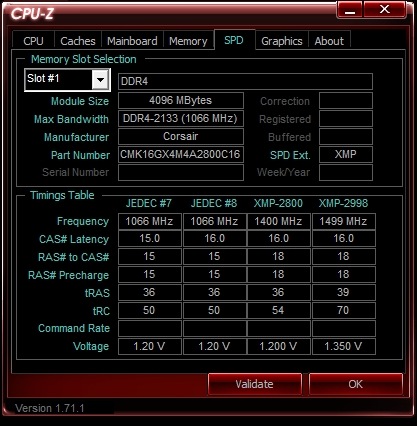 Pay attention to the RAM timings (7-7-7-18) and voltage (1.5 V).
Product Preview
KOMPUTERBAY 2GB (2 x 1GB) DDR DIMM (184 PIN) 400Mhz PC3200 CL 3.0 DESKTOP MEMORY
- KOMPUTERBAY 2GB (2 x 1GB ) DDR DIMM (184 PIN) 400Mhz PC3200 CL 3.0 DESKTOP MEMORY
- WORKS ON MAC AND PC — 64×8 LOW DENSITY
- BRAND NEW 2 X 1GB PC3200 DDR 400 Mhz
- SUPPORTS DUAL CHANNEL 100% COMPATIBLE MEMORY CAPACITY: 2GB (2x1GB)
- Lifetime Warranty
DUOMEIQI 8GB Kit (4X 2GB) DIMM UDIMM PC2-6400U DDR2 800MHz PC2-6400 CL6 1.8v 240 PIN Desktop Memory RAM Module Fit for Intel AMD System Non-ECC Unbuffered
- ✅Model: Desktop ram pc2-6400 ddr2 800mhz udimm ram 2RX8 240 Pin Non-ECC Unbuffered Desktop ddr2 sdram. (Before installation, please wipe connection figure gently with eraser, don’t use Corrosives, like ethyl alcohol)
- ✅Note: please make sure your desktop motherboard model and the maximum ram before order
- ✅Connecting Finger: Advanced electroplating process is applied on the connecting finger of pc2 6400 ddr2 800mhz ram to improve corrosion resistance and electrical conductivity.

- ✅Multifunction: This ddr2 ram 8gb kit will increase bandwidth, improve system performance, reduce power consumption and extend battery life. Faster burst access speed for improved sequential data throughput, bring you great online and game experience.
- ✅WARRANTY SERVICE: Life-time warranty for your confidence purchase of this ddr2-800 udimm ram. Any problems, please feel free to contact us, we are here for you 24 hours.
Sale
Patriot 16GB(2x8GB) Viper III DDR3 1600MHz (PC3 12800) CL9 Desktop Memory With Black Mamba Heatsink — PV316G160C9K
- Capacity: 16GB (2 x 8GB) Kit
- DIMM Type: 240-Pin NON-ECC UDIMM
- Voltage: 1.5V
- Frequency: PC3-12800 (1600MHz)
- Timings: 9-9-9-24
How to calculate the maximum transfer rate for a memory module?
Figure 1: A DDR3-1333/PC3-10666 memory module
The maximum transfer rate for a memory module can be calculated through the following formula:
Maximum Theoretical Transfer Rate = clock x number of bits / 8
Since DIMM modules transfer 64 bits at a time, “number of bits” will be 64. As 64 / 8 equals 8, we can simplify this formula to:
Maximum Theoretical Transfer Rate = clock x 8
If the memory module is installed on a system where the memory bus is running at a lower clock rate, the maximum transfer rate the memory module will achieve will be lower than its theoretical maximum transfer rate. Actually, this is a very common misjudgment.
How do RAM memories work?
For example, let’s say that you bought a pair of DDR3-2133/PC3-17000 RAMs. Even though they are labeled as DDR3-2133, they won’t run at 2,133 MHz automatically on your system. This is the maximum clock rate they support, not the clock rate at which they will be running.
If you install it on a regular PC system supporting DDR3 RAM memories, they will probably run at 1,333 MHz (DDR3-1333) – which the maximum DDR3 RAM standard speed –, achieving a maximum transfer rate of 10,664 MB/s (or 21,328 MB/s if they are running under dual channel mode, read our tutorial on dual channel to understand more about this subject). So, they won’t automatically run at 2,133 MHz nor automatically achieve the 17,000 MB/s transfer rate.
Why should or shouldn’t you buy these modules?
So, why would someone buy these modules? Someone would buy them for overclocking. Since the manufacturer guarantees that these modules will run up to 2,133 MHz, you know that you can raise the memory bus clock up to 1,066 MHz to achieve a higher performance with your system. However, your motherboard must support this kind of overclocking (read our tutorial on memory overclocking for more details). Thus buying a memory module with a labeled clock rate higher than what your system supports is useless if you are not going to overclock your system.
For the average user, that is everything you need to know about DDR, DDR2, and DDR3 memories. For the advanced user, there is yet another characteristic: the temporization of the memory, a.k.a. timings or latency. Let’s talk about it.
RAM Timings
Because of timings, two memory modules with the same theoretical maximum transfer rate can achieve different performance levels. Why is this possible if both are running at the same clock rate?
Timings measure the time the memory chip delays doing something internally. Here is an example. Consider the most famous parameter, which is called CAS Latency (or CL or “access time”) that tells us how many clock cycles the memory module will delay in returning data requested by the CPU.
Understanding CL Memory Modules
A memory module with a CL 9 will delay nine clock cycles to deliver a requested data, whereas a memory module with a CL 7 will delay seven clock cycles to deliver it. While both modules may run at the same clock rate, the second one will be faster, as it will deliver data sooner than the first one. This issue is known as “latency.” As you can see in Figure 1, the module portrayed there has a CL of 7.
RAM timings explained
The RAM timings are given through a series of numbers; for instance, 4-4-4-8, 5-5-5-15, 7-7-7-21, or 9-9-9-24. These numbers indicate the amount of clock cycles that it takes the memory to perform a certain operation.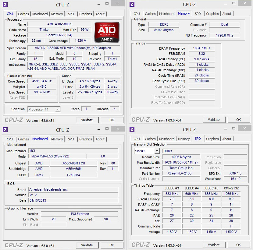 The smaller the number, the faster the memory. The memory module portrayed in Figure 1 has 7-7-7-18 timings, while the memory module portrayed in Figure 2 has 8-8-8-24 timings.
Figure 2: A DDR3-1600/PC3-12800 memory module with 8-8-8-24 timings
The operations that these numbers indicate are the following: CL-tRCD-tRP-tRAS-CMD. To understand them, bear in mind that the memory is internally organized as a matrix. This is where the data are stored at the intersection of the lines and columns.
- CL: CAS Latency. The time it takes between a command having been sent to the memory and when it begins to reply to it. It is the time it takes between the processor asking for some data from the memory and then returning it.
- tRCD: RAS to CAS Delay. The time it takes between the activation of the line (RAS) and the column (CAS) where the data are stored in the matrix.
- tRP: RAS Precharge. The time it takes between disabling the access to a line of data and the beginning of the access to another line of data.
- tRAS: Active to Precharge Delay. How long the memory has to wait until the next access to the memory can be initiated.
- CMD: Command Rate. The time it takes between the memory chip having been activated and when the first command may be sent to the memory. Sometimes this value is not announced. It usually is T1 (1 clock cycle) or T2 (2 clock cycles).
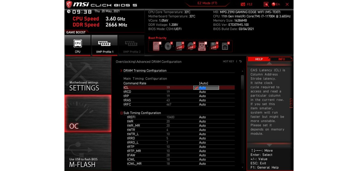
Usually, you have two options. The first one is to configure your PC to use the memory standard RAM timings, usually by setting memory configuration to “Auto” on the motherboard setup. The second one is to manually configure your PC to use lower memory timings.
Motherboard Timings
Notice that not all motherboards allow you to change the memory timings. Also, some motherboards may not be able to run at very low timings, and they may configure your memory module to run at a higher timing setting because of this.
Figure 3: Configuration of memory timings at the motherboard setup
How does overclocking work?
When overclocking your memory, you may need to increase the memory timings in order to make the system run in a stable manner. Here is where something very interesting happens. Due to the increased timings, the memory may achieve a lower performance, even though it is now configured to run at a higher clock rate, due to the latency that was introduced.
That is another advantage of memory modules sold specifically for overclocking. The manufacturer, besides guaranteeing that your memory module will achieve the labeled clock rate, also guarantees that you will be able to keep the labeled timings up to the labeled clock.
To understand things easier.
For example, even though you may achieve 1,600 MHz (800 MHz x2) with DDR3-1333/PC3-10600 modules, on these modules it may be necessary to increase the memory timings, while on DDR3-1600/PC3-12800 ones the manufacturer guarantees that you will be able to achieve 1,600 MHz keeping the labeled timings.
Now we are going a step further as we will explain in detail each one of the memory timing parameters.
CAS Latency (CL) Impact on RAM Speed
As previously mentioned, CAS Latency (CL) is the best known memory parameter. It tells us how many clock cycles the memory will delay returning the requested data. A memory with CL = 7 will delay seven clock cycles to deliver data, while a memory with CL = 9 will delay nine clock cycles to perform the same operation. Thus, for two memory modules running at the same clock rate, the one with the lowest CL will be faster.
A direct example
Notice that the clock rate here is the real clock rate under which the memory module is running – i.e., half the rated clock rate. As DDR, DDR2, and DDR3 RAM memories can deliver two data per clock cycle, they are rated with double their real clock rate.
In Figure 4, you can see how CL works. We gave two examples, a memory module with CL = 7 and a memory module with CL = 9. The command in blue would be a “read” command.
Figure 4: CAS Latency (CL)
A memory with CL = 7 will provide a 22.2% improvement on memory latency over a memory with CL = 9, considering that both are running at the same clock rate.
You can even calculate the time the memory delays until it starts delivering data. The period of each clock cycle can be easily calculated through the formula:
T = 1 / f
Thus, the period of each clock cycle of a DDR3-1333 RAM memory running at 1333 MHz (666.66 MHz clock) would be 1.5 ns (ns = nanosecond; 1 ns = 0.000000001 s). Keep in mind that you need to use the real clock rate, which is half of the labeled clock rate. So, this DDR3-1333 memory would delay 10.5 ns to start delivering data if it had CL =7, or 13.5 ns if it had CL = 9, for example.
Burst Mode explained
SDRAM, DDR, DDR2, and DDR3 RAM memories implement burst mode, where data stored in the next addresses can exit the memory at only one clock cycle. So, while the first data would delay CL clock cycles to exit the memory, the next data would be delivered right after. The prior data that has just come out from the memory, doesn’t have to wait for another CL cycle. Also, DDR, DDR2, and DDR3 memories deliver two data per clock cycle, and that is why they are labeled as having twice their real clock rate.
RAS to CAS Delay (tRCD) Impact on RAM Speed
Figure 5: RAS to CAS Delay (tRCD)
Each memory chip is organized internally as a matrix. At the intersection of each row and column, we have a small capacitor that is in charge of storing a “0” or a “1” – the data. Inside the memory, the process of accessing the stored data is accomplished by first activating the row and then the column where it is located.
RAS and CAS
This activation is done by two control signals called RAS (Row Address Strobe) and CAS (Column Address Strobe). The less time there is between these two signals the better, as the data will be read sooner. RAS to CAS Delay or tRCD measures this time. In Figure 5 we illustrate this, showing a memory with tRCD = 3.
As you can see, RAS to CAS Delay is also the number of clock cycles taken between the “Active” command and a “read” or “write” command.
As with CAS Latency, RAS to CAS Delay works with the memory real clock (which is half of the labeled clock). The lower this parameter, the faster the memory will be, as it will start reading or writing data earlier.
RAS Precharged (tRP) Impact on RAM Speed
Figure 6: RAS Precharged (tRP)
After data is gathered from the memory, a command called Precharge needs to be issued, closi
ng the memory row that was being used and allowing a new row to be activated. RAS Precharge time (tRP) is the time taken between when the Precharge command and the next Active command can be issued. As we learned from the previous page, the Active command starts a read or write cycle.
In Figure 6, we are giving an example of a memory with tRP = 3.
As with the other parameters, RAS Precharge works with the memory real clock (which is half of the labeled clock). The lower this parameter, the faster the memory will be, as it will issue the Active command earlier.
Adding everything we’ve seen, the time elapsed between issuing the Precharge command and actually getting the data will be tRP + tRCD + CL.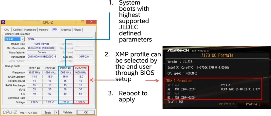
Other Parameters Impacting RAM Timings
Let’s take a better look at the other two parameters, Active to Precharge Delay (tRAS) and Command Rate (CMD). As with the other parameters, these two parameters work with the memory real clock (which is half of the memory labeled clock). The lower these parameters, the faster the memory will be.
- Active to Precharge Delay (tRAS): After an Active command is issued, another Precharge command cannot be issued until tRAS has elapsed. So, this parameter limits when the memory can start reading (or writing) a different row.
- Command Rate (CMD): It is the time taken by the memory chip from being activated (through its CS – Chip Select – pin) and when any command can be issued to the memory. This parameter carries the letter “T” with it. Possible values are 1T or 2T, meaning one clock cycle or two clock cycles, respectively.
Frequently Asked Questions
How fast should RAM be for a gaming PC?
For gaming, we recommend RAM modules that are as fast as possible, for obvious reasons. For starters, video games these days not only take up quite a lot of the RAM but also separate that data. This is why you’ll need your RAM to access everything as quickly as possible for a seamless experience. You should go for dual-channel DDR4 or DDR5 RAM with a frequency of 3,000 MHz or more. Those modules can get quite expensive, but it’s way better than experiencing bottlenecks during intense gameplay sequences.
Do timings matter on RAM?
Overall, we certainly found that if you dig deep enough, you’ll discover that timings definitely matter. It won’t impact every game or application. However, it does make sense to at least consider timings when buying RAM, especially if you can get better timings. With that said, we only recommend buying RAM from trusted brands and from trusted retailers.
2 Reasons why your warranty can be voided.
Even if a RAM module’s warranty lasts a lifetime in theory, in practice that warranty can be easily voided. This could happen from two factors.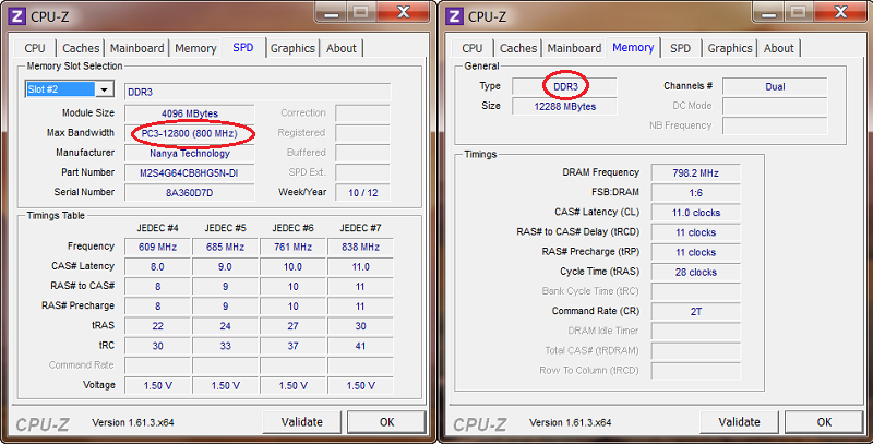 First, if someone has tampered with the module in the past the warranty will be voided. Second, if there’s too much goo or liquid present on it the same thing will happen.
Is RAM speed limited by CPU?
Actually, it is the combination of CPU and motherboard which limits DIMM speed. DIMM speed will only go as high as the lower of the speed limits between the CPU and motherboard. For example, a CPU may support speed up to 1600 while a motherboard supports speeds up to 2400. However, DIMMs will go up to 1600. In short, your computer is only as fast as its weakest component.
Last update on 2023-02-25 at 06:06 / Affiliate links / Images from Amazon Product Advertising API
An Overview of CAS (Column Access Strobe) Latency RAM
- MiniTool
- MiniTool Wiki Library
- An Overview of CAS (Column Access Strobe) Latency RAM
What Is CAS Latency
CAS (Column Access Strobe) latency refers to the delay time between the READ command and the time data gets available.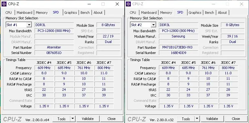 The CAS latency is also called CL. You will see a list of timing on the RAM like CL16-18-38 and CL14-14-34. The number behind the CL stands for the RAM kit’s CAS latency.
Tip: For more information about CAS latency RAM, please continue reading this post of MiniTool.
How the CAS latency RAM is measured? The interval is specified in nanoseconds (absolute time) in asynchronous DRAM. Differently, the interval is specified in clock cycles in synchronous DRAM.
-image from reddit.com
As the latency is associated with plenty of clock ticks rather than absolute time, the exact time for an SDRAM module to respond to a CAS event may vary because of different uses of the same module. What does RAM CAS latency mean? Keep reading the following content to learn the details.
Recommended reading: How Much RAM Can My Computer Take? Check the Maximum RAM Now!
What Does CAS Latency Mean
The RAM module’s CAS (Column Address Strobe) latency is how many clock cycles the RAM takes for accessing the specific set of data in one of its columns and making the data available on its output pins.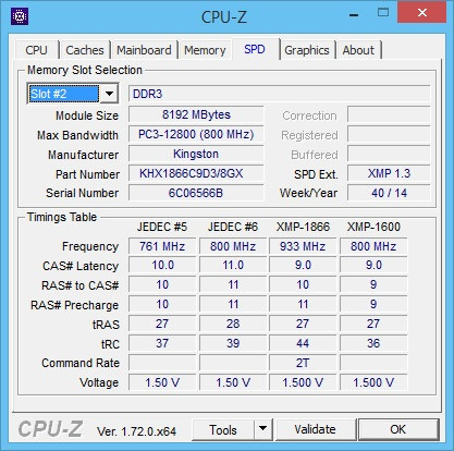
Generally speaking, a RAM kit with a CAS of 16 takes 16 RAM clock cycles to finish this task. In other words, the lower the CAS latency is, the less RAM is required. In addition, you should also note that the CAS latency can be described via several ways. To be specific, a RAM kit with a CAS latency of 16 can be written as CAS 16 or CL16.
Moreover, two different RAM kit may have the same data transfer rate. For instance, both the Team Group Delta Tuf Gaming RGB DDR4-3200 and G.Skill Trident Z Royal DDR4-3200 have a transfer rate of DDR4-3200.
Top recommendation: RAM vs ROM: The Key Differences Between the Two Memory
RAM Latency vs RAM Speed
The data transfer rate of RAM tells you how many mega transfers (1, 000, 000 data transfers) the RAM within one second. For example, a DDR4-3200 RAM can deliver 3200 mega transfers per second.
What about RAM CAS latency? It can help you learn the performance of RAM as well. As mentioned earlier, the CAS latency RAM tells the number of clock cycles it takes for the RAM to send data.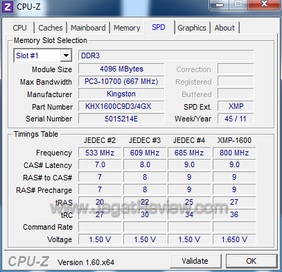 At the same time, you should also consider the duration of each cycle to obtain an overview of RAM’s total latency.
RAM latency vs RAM speed: which one is more vital? Analyzing from the above description, you can find that both the RAM latency and RAM speed are important for RAM.
Though the DDR4 RAM is newer and has better storage density and power efficiency compared with DDR3 RAM, it has higher CAS latency. According to investigation, DDR3 usually has a CAS latency of 9 or 10, while the DDR4 has at least 15 CAS latency. Thanks to faster clock speeds, the DDR4 has a better overall performance than DDR3.
You may also be interested in this: What Are the Differences Between DDR3 and DDR4 RAM
After reading the post, you may learn what CAS latency RAM is and some addition information about it. Hence, you will get a comprehensive understanding of CAS latency RAM as long as you finish reading. Hope this post can be helpful for you. Here comes the end of the article.
What are RAM timings
Top
04/29/2022
Author: Dmitry Mukharev
1 star2 stars3 stars4 stars5 stars0004 1
88
We understand what RAM timings are and what they mean.
The performance of the entire computer largely depends on the speed of the RAM, so its choice is no less important than buying the «right» processor or motherboard. Well, among the most important parameters of any RAM, frequency and timings stand out. But if everything is clear from the first, then the timings for many remain a dark forest. Today we will tell you what is hidden behind this incomprehensible set of numbers, and what meaning it has.
Contents
- What are timings
- What are the timings
- How to find out RAM timings
- How to choose the fastest RAM
Speaking in a very simple language, RAM is an array with a two-dimensional table, the cells of which store the necessary information. And arrays with cells of the same size, in turn, are combined into so-called banks.
To perform any operation on the data in this table, the controller and the memory chip require a certain number of memory bus clock cycles.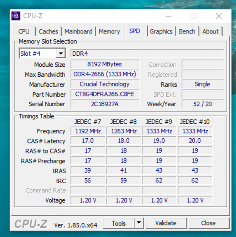 Well, timing is the number of such cycles, or the number of cycles by which the execution of a certain memory operation will be late. Hence the name itself — timing or delay.
-
Purchase
How to choose RAM: we understand the nuances
Actually, that is why two RAMs with the same frequency, but different timings will work differently, and the memory with the lowest delay will be the fastest.
Each operation with RAM can be divided into several stages. Therefore, the characteristics of any RAM bar indicate several timings — delays that occur at a certain stage of working with memory. Timing numbers indicate the following operations:
CL: CAS Latency — the number of clock cycles that elapse from sending a request to memory until the start of a response to it.
tRCD: RAS to CAS Delay — the number of ticks that the controller needs to activate the desired line of the bank.
tRP: RAS Precharge – the number of cycles for charging and closing one row, after which the next row can be activated.
tRAS: Row Active Time — the minimum number of cycles during which the row will be active. It cannot be closed before this time.
All these timings are specified in the RAM parameters in the exact order that we have given. Take, for example, Patriot Memory VIPER STEEL DDR4-3733 CL-17 21-21-41 RAM. We see that it belongs to the DDR4 type and operates at a clock frequency of 3733 MHz. It takes 17 cycles to start responding to an incoming request (CL). Activation of the desired row takes 21 cycles (tRCD) and the same number of cycles is spent on its closing and activation of the next row (tRP). Moreover, the line itself can be closed no earlier than after 41 cycles (tRAS).
As you can see, each number in the name of the RAM has its own meaning. And, having understood this, you can easily choose the most suitable RAM for you.
-
Purchase
5 best RAM options for overclocking
RAM timings can be viewed on its page in any self-respecting store or on the manufacturer’s website. If you want to see the characteristics of the memory you already have installed, you can use CPU-Z or similar utilities.
In short, the frequency of RAM is more important than timings, but at the same frequency, the RAM with the lowest delay will be the fastest. Actually, it is on the basis of this that it is worth choosing the most suitable RAM strips for you. In general, this algorithm looks like this:
- Decide on the type of RAM that your computer supports — DDR3, DDR4, DDR5, etc.

- Decide on the amount of memory you need.
- Find out what RAM frequency your PC processor and motherboard support.
- Choose RAM sticks that work at the maximum frequency available for your computer.
- Among these bars, choose models with minimum timings.
Read also
- Squeezing the juice out of the PC: memory overclocking
Tags
RAM
Author
Dmitry Mukharev
Was the article interesting?
Share link
By clicking on the «Subscribe» button,
you consent to the processing of personal data
Recommended
Advertising on CHIP
Contacts
Timings (latency) of RAM, how to find them and which ones are better for DDR4, DDR3 (table), how to view them on a PC and laptop
memory — lower timings or higher frequency
In this article we will understand what RAM timings are. We will find out which latency parameters are best for speed and how to view them on a computer or laptop. We will understand how to choose and set the timings of the RAM correctly and what they affect. I will give a link to the timing calculator and a table for the main types of memory and frequencies.
Usually when choosing RAM for a desktop or laptop, we look at the amount of RAM, clock speed, and type of DDR memory for compatibility with the motherboard. However, the RAM also has such a characteristic as timings or, scientifically, latency. And only specialists and advanced gamers pay attention to this parameter.
The higher the frequency and lower the timings, the faster the RAM works.
Dealing with the basic timings
Latency (from the English. CAS Latency abbreviated as CL) in everyday life “timing” is the time delays that occur when the central processor accesses the RAM.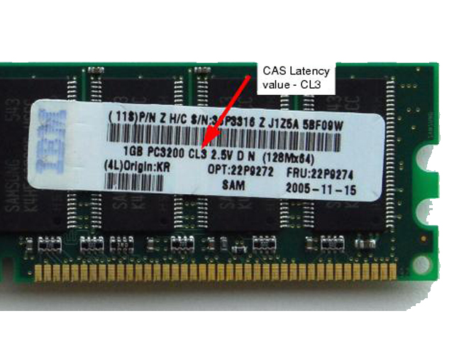 These delays are measured in memory bus cycles.
The lower the timings, the faster the data exchange between the processor and memory, and therefore the more efficient the RAM.
Each time delay has its own name and is responsible for the transmission rate of certain data.
In the technical specifications of RAM, they are written in strict sequence in the form of three or four numbers:
CAS Latency, RAS to CAS Delay, RAS Precharge Time and DRAM Cycle Time Tras / Trc (Active to Precharge Delay). Abbreviated it may look like this: CL-RCD-RP-RAS.
Most manufacturers indicate the timings in the markings on the memory modules. It can be 4 digits, for example: 9-9-9-24, or only one, for example CL11. In this case, the first parameter is meant, that is, CAS Latency.
Now let’s look at these delays in more detail.
For an illustrative example, let’s take a pair of DDR3 1600 MHz memory sticks, 8 Gb each with timings 11-11-11-28.
On the memory bar, this information is stored in the SPD chip and is available to the motherboard chipset. You can view this information using special utilities, such as CPU-Z or HWINFO.
Memory timings in CPU-Z and HWINFO programs
CAS Latency (tCL) — the most important timing in memory operation, which has the greatest impact on its speed. In the characteristics of memory is always the first. Indicates the period of time that elapses between the issuance of a command to read / write information and the start of its execution.
This time can be measured in nanoseconds. The best way to do this is to use a calculator. We enter the frequency in MHz (we have it 1600) and the delay time (11). At the output, we get that the delay time between the issuance of a command to read / write data and the start of its execution is 13.75 nanoseconds.
RAS to CAS Delay (tRCD) — Delay from RAS to CAS. The time that must pass from the moment the matrix row (RAS) is accessed to the time the matrix column (CAS) is accessed, in which the required data is stored.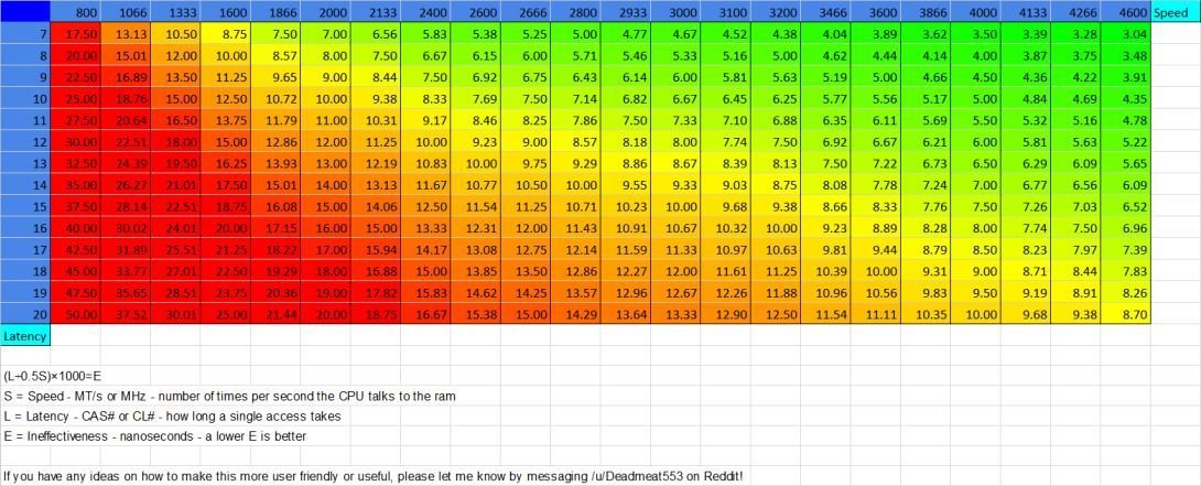
RAS Precharge Time (tRP) — time interval from the moment when access to one matrix line is closed and access to another data line begins.
Row Active Time (tRAS) — the pause that memory needs to return to the state of waiting for the next request. It defines the ratio of the interval during which a row is open for data transfer (tRAS — RAS Active time) to the period during which a full cycle of opening and updating a row (tRC — Row Cycle time), also called the bank cycle (Bank Cycle Time) is completed. ).
Command Rate — command rate. The time from the moment the memory chip is activated until the moment when the memory can be accessed with the first command. Often this parameter is not indicated in the memory marking, but it is always in programs. Usually it is T1 or T2. 1 or 2 clock cycles.
How to change
Timings can be changed both downwards and upwards by overclocking. This requires fine tuning of the frequency of the module and its voltage. By decreasing or increasing the frequency of the memory, timings also decrease or increase. These parameters are selected individually for each memory module or memory sets.
Here is one of the comments on the memory I mentioned above ⇓
Memory is very worthy! From a base frequency of 1600 mhz, it was possible to overclock to 2200 mhz with timings of 11-12-12-28 at a voltage of 1.65v.
Frequency overclocking was 27%, which is a very good result. At the same time, timings and voltage were increased minimally. Such overclocking had a rather noticeable effect on the entire speed of the computer.
The whole point of this action is to choose such optimal characteristics of frequency, timings and voltage so that the memory module / modules give the maximum speed and at the same time work stably in this mode. It takes time and knowledge.
Also, the motherboard must support overclocking of the RAM. Now there are memory sticks with a built-in XMP profile.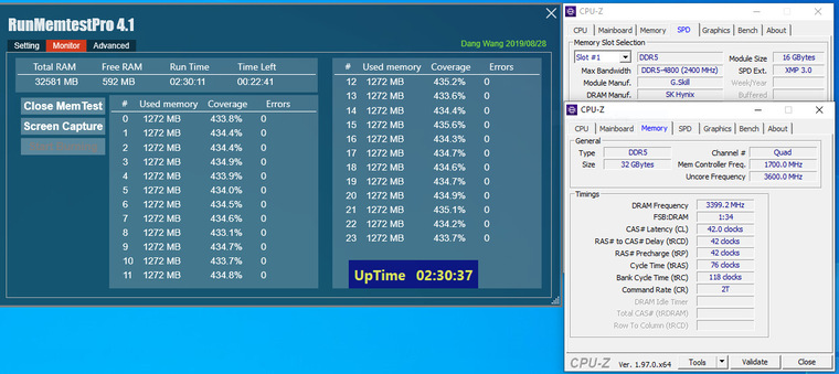 It already contains factory overclocking parameters with which the memory can work. You just have to apply the desired XMP profile and the RAM will start with these parameters.
In normal mode, the computer receives all the RAM settings from the SPD — a microcircuit that is soldered on each module. But, if there is a desire to achieve maximum performance, it is advisable to try changing the timings. Of course, you can immediately purchase modules with minimal delays, but they can cost significantly more.
Memory settings are changed through the BIOS of a PC or laptop. There is no universal answer to the question of how to change the timings of RAM in the BIOS.
Memory subsystem configuration options can vary greatly from motherboard to motherboard. Cheap motherboards and laptops may only have memory running in the default mode, but there is no possibility to choose RAM timings.
Expensive models may have access to a large number of settings, in addition to frequency and timings.
These parameters are called sub-timings. They can be useful when fine-tuning the memory subsystem, for example, during extreme overclocking.
Changing timings can improve computer performance. For DDR3 memory, this is not the most important parameter and the increase will not be too large, but if the computer works a lot with heavy applications, you should not neglect it. This fully applies to the more modern DDR4.
Memory overclocking can have a noticeably greater effect, and in this case the timings will most likely have to be increased rather than lowered in order to achieve stable operation of memory modules in freelance mode.
By the way, similar recommendations can be found when choosing memory for new AMD Ryzen processors. Tests show that in order to unleash the potential of these processors, memory with maximum frequencies is needed, even at the expense of timings. Here is a timing calculator for Ryzen processors.
It should be noted that tuning the memory subsystem will not give any noticeable result in all cases. There are applications for which only the amount of RAM is important, and fine tuning of delays will give an increase at the level of error.
Keep in mind that reducing memory latency too much can lead to unstable computer operation and even to the fact that it refuses to start. In this case, you will need to reset the BIOS to default settings or, if you do not know how to do this, you will have to contact specialists.
How to correctly set
Of course, it’s worth starting with finding out the standard settings recommended by the manufacturer for this module. How to check the timings of RAM, we reviewed earlier. Then you can look at the statistics on the Internet resources dedicated to overclocking, to roughly understand what you can expect from a particular RAM module.
As noted, incorrect delay values can easily make your computer unbootable, so find out exactly how BIOS resets are performed. Moreover, not only software, but also hardware, in case it is not even possible to enter the BIOS.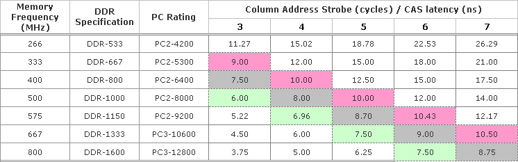 Information about this can be found in the documentation for the motherboard or on the Internet.
It usually doesn’t take much time to figure out how to set the RAM timings in the BIOS. The first time you may need documentation, then everything will be easier.
Next is to test how the system behaves under load. To do this, you can use specialized programs or simply load the computer well, for example, launch a game with high graphics settings for an hour or encode a high-resolution video file.
If the computer is stable, you can lower the timings by one more clock cycle. If hangs occur, system error messages appear, or programs crash, then you need to undo the changes and go back a beat.
Having figured out how to correctly reduce the timings of ddr3 and more modern ddr4 RAM, you should not immediately start experimenting. First, it is worth determining, based on the characteristics of your hardware, which is preferable: increase frequencies or lower delays.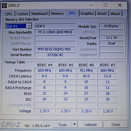 Now, in most cases, a greater effect can be achieved by increasing the clock frequencies.
What affects the speed of RAM more — lower timings or higher frequency
The most important thing that you must understand and remember in order to understand this issue once and for all, is that WHEN INCREASING THE FREQUENCY AT WHICH THE RAM MODULE IS WORKING, MEMORY DELAYS AUTOMATICALLY INCREASE. As the frequency decreases, they decrease. This is clearly seen when comparing memory sticks of different generations.
To compare the speed of work, let’s take two different types of RAM. Older DDR3 and modern DDR4.
Comparison of timings for DDR4 and DDR3 9 RAM0004 You can compare the speed of different RAM modules in nanoseconds using the formula ⇓
Timing * 2000 / memory frequency. For example, a DDR4 stick with CL16 timing will run at 16*2000/3000= 10.6 nanosec , and a DDR3 stick with CL9 timing at 9*2000/1600= 11.
25 nanosec .
As can be seen from the example, the memory frequency is also very important. DDR3 has a much lower latency than DDR4, but the frequency of the DDR4 module is noticeably higher than DDR3. Although not by much, DDR4 is ahead of DDR3 in terms of speed. It also has a large throughput. In the future DDR5, I think the difference in speed will be even greater.
It turns out that the clock speed of the RAM affects performance to a greater extent than lower timings. Of course, if the choice is between bars with the same frequency, then it is better to choose the one with lower delays.
If someone wants to take a closer look at this issue, here is a link to the timings table in Googledox.
Timings should also be taken into account when choosing memory modules for multichannel mode. The best solution would be to buy a ready-made kit in which all the bars have identical characteristics. If this is not possible, then you should look for modules that not only have the same clock frequency and organization of chips, but also have the same timings.