Intel’s NUC 11 Essential Arrives With 10nm Jasper Lake CPUs
Skip to main content
When you purchase through links on our site, we may earn an affiliate commission. Here’s how it works.
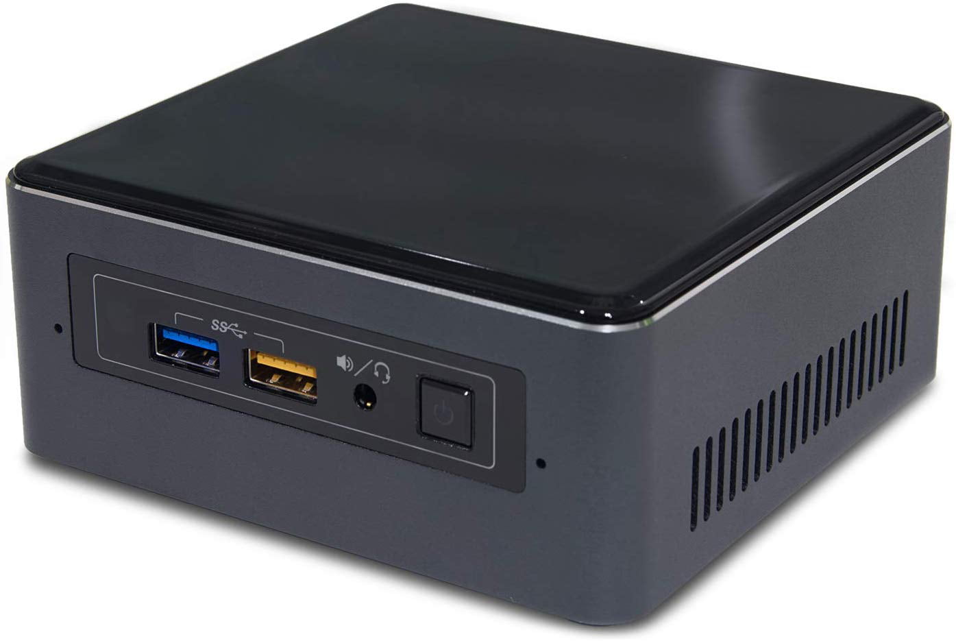
Intel NUC 11 Essential
(Image credit: FanlessTech)
The specifications for Intel’s NUC 11 Essential (Atlas Canyon) device have emerged, courtesy of FanlessTech . The upcoming NUC utilizes the chipmaker’s 10nm low-powered Jasper Lake processors.
Armed with Tremont cores, Jasper Lake checks in with thermal limits between 6W and 10W, so it doesn’t require any serious cooling. The NUC 11 Essential will be available with three different processor options. The Pentium Silver J6005 and Celeron J5105 are quad-core parts, while the Celeron J4505 is a dual-core chip. Neither processor leverages Hyper-Threading technology.
Intel outfitted the NUC 11 Essential with two SO-DIMM memory slots so you can pair either Jasper Lake processor with up to 16GB of DDR4-2933 memory at 1. 2V. Some select models will come equipped with 64GB of eMMC storage, but the NUC 11 Essential offers a single M.2 2280 slot for housing NVMe and SATA drives.
As FanlessTech has noted, this is the first time that an entry-level NUC is arriving with a M.2 slot as opposed previous designs with spacing for a 2.5-inch drive. This helps trim down the size of the NUC as the NUC 11 Essential has a 135x115x36mm footprint.
Intel NUC 11 Essential (Image credit: FanlessTech)
The NUC 11 Essential lands with one HDMI 2.0b port and one DisplayPort 1.4 output. Both connectors support HDCP 2.2 as well as 4K monitors, so you can connect up to two 4K displays to the NUC 11 Essential. You’ll still be limited by Jasper Lake’s Intel UHD graphics engine. The iGPU is an abysmal gaming performer, but should be sufficient for conventional workloads.
The NUC 11 Essential only has a single Gigabit Ethernet port. If you’re a wireless aficionado, however, you can take advantage of the speedy Wi-Fi 6 AX101 and Bluetooth 5. 2 connectivity on the NUC. There are two 3.5mm audio connectors on the front of the device. The NUC 11 Essential supports 7.1-audio through the HDMI port.
Don’t let the NUC 11 Essential’s small body fool you. The device offers enough connectivity options to be your daily driver. There are two front USB 3.1 ports, two rear USB 3.1 ports, and two rear USB 2.0 ports. The NUC sips power through a standard 19VDC 65W power supply.
Intel backs the NUC 11 Essential with a limited three-year warranty. There was no mention of pricing. According to FanlessTech, the NUC won’t arrive until the first quarter of next year.
Get instant access to breaking news, in-depth reviews and helpful tips.
Contact me with news and offers from other Future brandsReceive email from us on behalf of our trusted partners or sponsors
Zhiye Liu is a Freelance News Writer at Tom’s Hardware US. Although he loves everything that’s hardware, he has a soft spot for CPUs, GPUs, and RAM.
Tom’s Hardware is part of Future US Inc, an international media group and leading digital publisher. Visit our corporate site .
©
Future US, Inc. Full 7th Floor, 130 West 42nd Street,
New York,
NY 10036.
Intel Launches NUC 11 Essential Kits With Jasper Lake 10nm SoCs
Skip to main content
When you purchase through links on our site, we may earn an affiliate commission. Here’s how it works.
(Image credit: Intel)
Intel’s NUC 11 Essential Kits, previously codenamed «Atlas Canyon», have now officially launched. These are low-power NUCs for entry level computing and not normally on the radar of PC enthusiasts, but the new 10nm Tremont based Jasper Lake SoCs inside can deliver a significant CPU and GPU performance uplift vs previous generations. Rough comparisons from Intel, to whet your appetite, indicate that Jasper Lake CPU cores are around 33% faster than Gemini Lake, and the GPU is even more convincing delivering up to a 78% uplift.
(Image credit: Intel)
We first reported on Atlas Canyon NUCs last May, when a product data sheet was unearthed and shared by Fanless Tech. At the time the source tipped a release of Q1 2022, and this has turned out to be accurate.
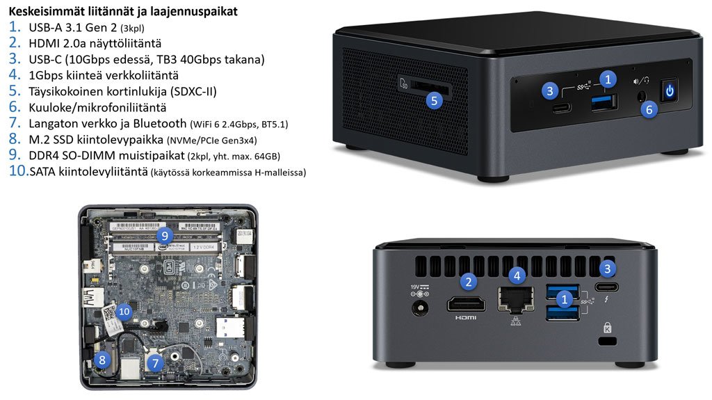
Pondering over the new Intel NUC 11 Essential Kits, you can see there are three CPU choices available to would-be buyers of the five newly launched SKUs. The choice is basically between barebones, full systems and bare boards with the Intel Celeron Processor N4505 with 2C/2T at up to 2.90 GHz, Intel Celeron Processor N5105 with 4C/4T at up to 2.90 GHz, or Intel Pentium Silver N6005 Processor with 4C/4T at up to 3.30 GHz. These processors are all 10W parts with Intel UHD graphics. WhIle the Celerons support up to 16GB of RAM, the Pentium is capable of supporting 32GB of DDR4-2933 via two SO-DIMM slots. Unsurprisingly, the Pentium has the best GPU too, with 32 Execution Units helping it stand out from the Celerons with 16 or 24EUs. Storage is via one M.2 2280 SSD, plus an optional 64GB eMMC.
(Image credit: Intel)
Considering the fuller system specs, one of these Intel NUC 11 Essential Kits measures 135 x 115 x 36mm like the classic compact low-power NUCs before it.
Ports/connectivity features include 1x DP1.4 and 1x HDMI 2.0b video outputs for dual displays, six USB ports (2 x front and 2 x rear USB 3.2; 2 x USB 2.0), 1 x 3.5mm stereo out jack, 1 x 3.5mm microphone jack, 10/100/1000 LAN, Intel Wireless-AC 9462 + Bluetooth 5.0. A barrel power jack takes input from the 65W 19V DC power brick. These systems are designed to support Windows 10, 11, and Linux distros.
Previous gen entry level NUCs started at around $200 for a bare bones offering with the cheapest CPU option, hopefully this will also be the starting price for the Atlas Canyon NUCs. We don’t have an availability date to share but these low-power NUCs should start to show up at retailers and etailers soon.
Get instant access to breaking news, in-depth reviews and helpful tips.
Contact me with news and offers from other Future brandsReceive email from us on behalf of our trusted partners or sponsors
Mark Tyson is a Freelance News Writer at Tom’s Hardware US. He enjoys covering the full breadth of PC tech; from business and semiconductor design to products approaching the edge of reason.
Topics
Systems
CPUs
Tom’s Hardware is part of Future US Inc, an international media group and leading digital publisher. Visit our corporate site .
©
Future US, Inc. Full 7th Floor, 130 West 42nd Street,
New York,
NY 10036.
What is 10 nm, 7 nm or 5 nm in a smartphone? Technical process for «dummies»
Rating of this article according to readers:
4.8
(547)
The appearance of this article on Deep-Review was only a matter of time. Many readers asked the same questions, the essence of which boiled down to the following: what does this figure (12, 10, 7 or 5 nm) really reflect in the technical characteristics of smartphones, where are those same 5 nanometers in the processor? What is a technical process in general and which processor is better to choose?
Even in modern printed books, there is a common misconception that these numbers indicate the size of the transistors that make up the processor.
In general, it’s time to deal with this issue!
I immediately warn you that the article is intended for the widest range of readers, that is, if you wish, even children can understand everything that has been said.
But before we talk about nanometers and the process technology, we need to understand the transistor. Without an understanding of this device, our entire further conversation will be meaningless.
What is a transistor in a smartphone processor? How does it work and why is it needed at all?
The transistor is the basis of any processor, memory and other microcircuits. It is a tiny device capable of operating in two modes: amplifying or switching an electrical signal. We are interested in switch mode .
The basis of any computer technology is ones and zeros. Watching videos on a smartphone, listening to music, augmented reality and neural networks all work on “ones and zeros”:
- One — there is current
- Zero — no current
We use transistors to get ones and zeros. When current comes out of this miniature device, we say that it is one, when there is no electrical signal, we get zero.
Accordingly, one transistor is completely useless nonsense that cannot do anything. Even to calculate 2+2 we need dozens of transistors.
So, to create a transistor, we take a little bit of sand (conditionally, some part of one grain of sand) and make a microscopic base out of it:
This will be our silicon substrate (silicon is obtained from sand). Now you need to draw two areas on this base. I thought about whether it is worth diving into the physics of this process and explaining how these areas are made and what happens there at the electron level, but I decided not to overload the article with unnecessary information. So let’s abstract a little.
So, we make two areas: we apply current to one (input to the transistor), and read from the other (output):
We made these areas inside the silicon substrate in such a way that the current could not pass from the input to the output.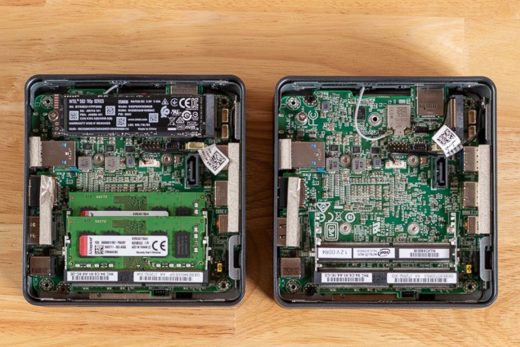 It will be stopped by the silicon itself (shown in green). In order for the current to pass from the input to the output along the surface of the silicon substrate, you need to place a conductive material (say, metal) on top and isolate it well:
And now the most important thing! When we apply voltage to this isolated piece of metal placed over a silicon substrate, it will create an electric field around itself. Insulation will not affect the action of this electric field in any way. And here all the “magic” happens: the silicon layer under the influence of this electric field begins to conduct current from the input to the output! That is, when we apply voltage, current can easily flow between the two areas:
That’s it! The only thing left is to connect the “wires” (electrodes) to the input, output and a piece of insulated metal, with which we will turn on / off the transistor. Let’s call them like this:
- Input — Source
- Output — Drain
- Metal with insulation — Gate
MOSFET
So, the transistor is energized, that is, electricity is supplied to source . But there is no current on the gate, since our transistor did not “come one”. Accordingly, the gate “closed” the transistor and the current cannot pass through it further, so at the output of the transistor we get zero :
Now the situation has changed and a voltage appeared on the gate of the transistor, which created an electric field that allowed the current to pass through the transistor from source to drain. As a result, the transistor gave out units (there is an electrical signal):
That’s how simple it is! That is, the main voltage is input to all transistors, but whether each specific transistor will pass this current further depends on the insignificant gate voltage. This voltage can appear, for example, when another transistor connected to this one sent an electrical impulse (“one”).
This knowledge is more than enough to answer all other questions regarding nanometers and the logic of the processor.
What physical processes are behind such a simple switch, that is, what exactly makes electrons pass through silicon when an electric field appears above it, I will not tell. Perhaps we will talk about doping silicon with phosphorus and boron, p-n junctions and electric fields some other time. And now let’s move on to the main question.
What is a process technology or where are these «7 nanometers» hidden?
Suppose we have a modern smartphone with a 7nm processor. What inside such a processor has a size of 7 nanometers? I suggest you choose the correct answer:
- Transistor length
- Transistor width
- Distance between two transistors
- Gate length
- Gate width
- Distance between gates of adjacent transistors
Whichever option you choose, your answer is incorrect because none of the above is of that size. If I asked the same question 20 years ago, the correct answer would be gate length (or channel length , through which current flows from drain to source ):
Stop! Channel length, width, area — but what’s the difference what is measured in what!? Why did they come up with these names of technical processes at all, why do ordinary people need them? What should the technical process show to an ordinary buyer? Why would he need to know the same transistor gate length?
A long time ago, a man named Gordon Moore (the founder of Intel Corporation) was wondering how fast technology was advancing.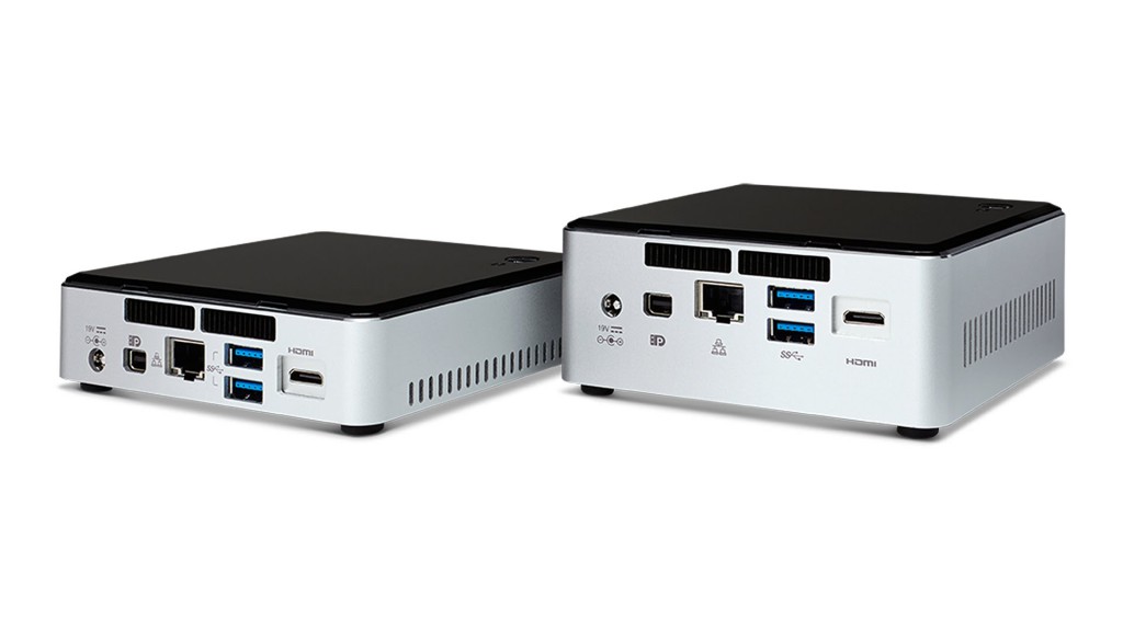 By the word «development» he meant an increase in the number of transistors that fit in the same area. The fact is that this indicator directly affects the calculation speed . A processor with only 1 million transistors will run much slower than one with 10 million transistors inside.
Moreover, by reducing the size of the transistor, its power consumption is automatically reduced ( the current passing through the transistor is proportional to the ratio of its width to its length ). The shutter size and capacitance are also reduced, allowing it to switch even faster. In general, some pluses!
So, this person was watching the history of computer technology and noticed that the number of transistors on a chip doubles approximately every 2 years . Accordingly, the sizes of transistors are reduced by the root of two times.
In other words, multiply each side of the square transistor by 0.7 to halve its area:
This observation was called «Moore’s law» and so the marking of the technical process was born: every two years this figure was multiplied by 0. 7 . For example, when switching from a 1000-nm process technology to a 700-nm process technology, the number of transistors on a chip increased by 2 times. Approximately the same can be said about all modern processors: 14 nm -> 10 nm -> 7 nm -> 5 nm. We simply multiply each subsequent generation by 0.7, assuming that the number of transistors there doubled.
I repeat, up to a certain point this figure meant channel length (or gate length), since these elements decreased in proportion to the size of the transistor.
But then it was possible to shorten the length of the gate faster than other parts of the transistor. Since then, it has become not entirely correct to associate the gate size with the technical process, since this no longer reflects a real increase in the density of transistors on a chip.
For example, the 250nm process had a gate length of 190nm, but the transistors were not packed so tightly compared to the previous process to call it 190nm (shutter size).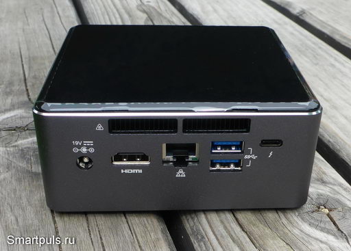 This would not reflect the actual density.
Then the length of the canal did not decrease at all every two years, as a new problem appeared. With a further decrease in the channel length, the electrons could bypass the narrow gate, since the blocking effect was not strong enough. Moreover, such leaks occurred constantly, causing increased power consumption and heating of the transistor (and, as a result, the entire processor).
In general, the technical process was untied from the length of the gate and they simply took a group of several transistors (the so-called cell ) and the area of this cell was used for the name of the process.
For example, in a 100-nm process technology, a cell of 6 transistors occupied, say, 100,000 nanometers (this is a conditional figure from the head). The company worked hard to reduce the size of transistors or increase the density of their placement, and after a couple of years, the same cell occupied 50,000 nm in the new processor.
It doesn’t matter whether the size of the transistors has decreased or just managed to pack them more tightly (due to the reduction of the metal layer and other tricks), we can safely say that the number of transistors on a chip has doubled. This means that we multiply the previous process technology (100 nm) by 0.7 and get a brand new processor made using the 70 nm process technology.
However, when we got to the 22nm process, reducing the length of the gate was no longer realistic, since electrons would pass through this gate and the transistors would constantly pass current.
The solution turned out to be simple and ingenious — you need to take the channel through which the current passes and raise it up, above the silicon core, so that it completely passes through the gate:
Now the entire space through which the current flows is controlled by the gate, since it is completely surrounded. And earlier, as we can see, this shutter was located above the channel and created a relatively weak blocking effect.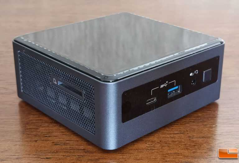
With the new technology, called FinFET, it was possible to continue to reduce the length of the gate and place even more transistors, as they became narrower (compare the channel width in the picture). But talking about the size of the transistor has become generally meaningless. It is not entirely clear even how to calculate these dimensions now, when the transistor has turned from a flat one into a three-dimensional one.
Thus, the technical process is completely “torn off” from any real values and simply conditionally indicates an increase in the density of transistors relative to the previous technical process.
For example, the channel length in a 14nm processor from Intel is 24nm, while Samsung’s is 30nm. Other metrics of these processors, which seem to be made according to the same technical process, also differ. Moreover, the length of the gate is not the smallest part of the transistor. In the same 14-nm processor, the channel width generally consists of several atoms and is 8 nanometers! That is, the technical process is not even a description of the smallest part of the transistor.
In other words, the nanometer process does not describe transistor sizes . Today, this is a conditional figure, meaning the density of transistors or an increase in the number of transistors relative to the previous technical process (which directly affects the speed of the processor).
In any case, it is important to remember a simple rule and use it when analyzing the characteristics of a smartphone:
A difference in the manufacturing process by 0.7 times means a twofold increase in the number of transistors
For example, we can look at the latest chips from Apple. The 10nm Apple A11 Bionic processor contains 4.3 billion transistors, and in the 7nm Apple A13 Bionic — 8.5 billion transistors. That is, we see that the technical process differs by 0.7 times, and the number of transistors — by 2 times. Accordingly, a 7nm processor is much more productive than a 10nm one.
Continuing the analogy, a 5nm processor should fit 2 times more transistors than a 7nm one! If this fact does not surprise you, be sure to read my note on the exponential development of technology at your leisure.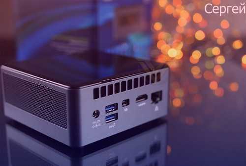
So, when you look at two smartphones with 14nm and 10nm processors, you know that the latter has a lot more transistors, and accordingly, its processing power is noticeably higher. So you should use the «technological process» when choosing a smartphone.
And if you are wondering how these soulless transistors can «think», do complex calculations, show movies or play music, then read the answers to these questions in our new material!
Alexey, chief. Deep-Review 9 Editor0022
P.S. Don’t forget to subscribe in Telegram to our popular science site about mobile technologies, so as not to miss the most interesting!
If you liked this article, join us on Patreon — it’s even more interesting there!
How would you rate this article?
Click on a star to rate it
There are comments at the bottom of the page…
Write your opinion there for all readers to see!
If you only want to rate, please specify what is wrong?
Intel makes a record leap in technology.
 It will move from 10nm chips to state-of-the-art 3nm chips
Technology
|
Share
In early 2023, Intel may release its first 3nm processor in collaboration with TSMC. This is a big step forward for her, as her own factories are designed for 10nm maximum. Intel has a design project ready for two such CPUs — one for servers and one for laptops. Together with her, Apple is also preparing for the transition to 3 nm — it plans to make it in the spring of 2022 with the release of a new modification of the iPad Pro tablet.
Intel accelerates its development
In 2023, Intel plans to launch production of processors manufactured according to the latest 3nm standards.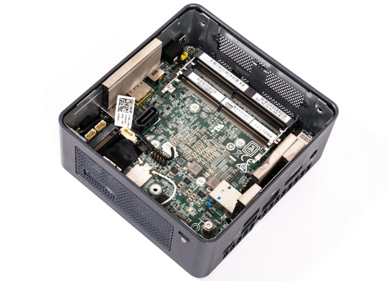 According to the Nikkei Asian Review, this is described in the company’s new development strategy. Now it produces its most advanced chips using the 10 nm process technology.
Intel will not be able to make such a giant leap on its own. Its future 3nm CPUs will be produced at its factories by the world’s largest chipmaker, TSMC. The first samples may see the light at the very beginning of 2023, although Intel and TSMC themselves have not yet confirmed this.
Intel has a design proposal for at least two 3nm chips. One of them is focused on laptops, and the second will be used in servers. Why Intel has not yet developed a desktop chip design is unknown, but the company is going to book a significant portion of TSMC’s orders for 3nm products.
In a year and a half, Intel processors will move to an ultra-modern process technology that no one else has
According to TSMC itself, the transition to a 3nm topology will increase processor performance by 10-15% compared to the current 5nm chips.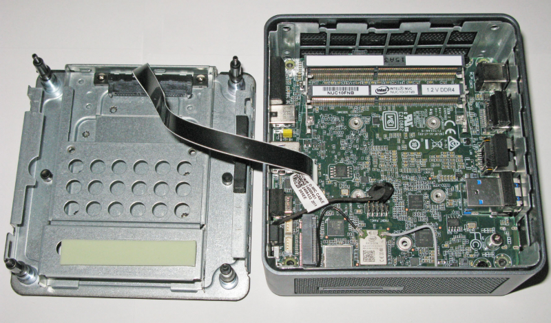 They first appeared at the end of 2020, and at the time of publication of the material, the number of devices in which they are used remained insignificant. The new technical process will reduce energy consumption by processors by 25-30%.
How Intel will get to 3 nanometers
Collaboration with TSMC is part of Intel’s new strategy to strengthen its position in the processor market and regain technical leadership. Its main competitor, AMD, has been producing 7nm chips for a long time and is preparing for the transition to 5nm with the help of the same TSMC.
As part of its strategy, as reported by CNews, Intel intends to develop partnerships not only with TSMC, but also with Taiwanese UMC, American GlobalFoundries and Korean Samsung. All of them are among the main chip manufacturers in the world market.
At the same time, Intel itself also has its own factories for the production of processors, but here it still lags far behind TSMC. Its factories are designed for a maximum of 10 nm.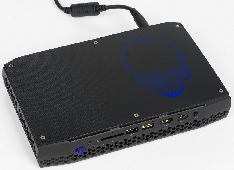
Intel still only dreams of mastering 7nm — a process technology that has been in the asset of TSMC for many years. The company is going to invest $20 billion in two related factories, and it intends to release the first such chips in 2023.
Intel will not be the first
Intel isn’t the only one showing interest in new manufacturing standards. According to the publication, Apple is going to share all the production volumes of new microcircuits with it.
It is possible that Apple will be the first company to announce a ready-to-serial production device based on a 3-nanometer chip. This happened with 5 nm — the world’s first such CPU (Apple A14) in September 2020 received the fourth-generation iPad Air tablet, and a month later — iPhone 12 smartphones. Prior to MacBook laptops and the Mac mini nettop, 5-nanometer CPUs represented M1 arrived in November 2020
How can banks switch to import-independent DBMS 9 in just a year0003
IT in banks
As the profile resource MacRumors writes, it will not be necessary to wait until 2023 for the appearance of the first 3-nanometer Apple chips, unlike Intel.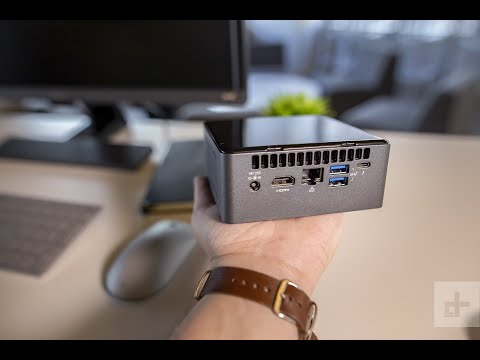 On the basis of such a processor, the iPad Pro 2022 tablet can be built, which Apple has not yet commented on any information about the development of.
Traditionally, Apple releases new versions of the iPad Pro tablet almost every year in early or mid-spring. When exactly the premiere of the iPad Pro 2022 will take place remains a mystery, but if nothing changes, then less than a year remains to wait for the announcement of the world’s first gadget on a chip with a 3 nm topology.
It is not yet known what kind of processor Apple is developing. It is possible that this will be a common chip for a whole series of its devices, because the new iPad Pro 2021 runs on the M1, which was originally created for laptops and nettops of the company. Also, M1 is now used in the desktop all-in-one iMac 2021.
Battle for 2 nm
Apple can get ahead of Intel not only in the release of the first 3 nm chips. In March 2021, CNews wrote that it is providing comprehensive assistance to TSMC in the development of a 2nm process technology.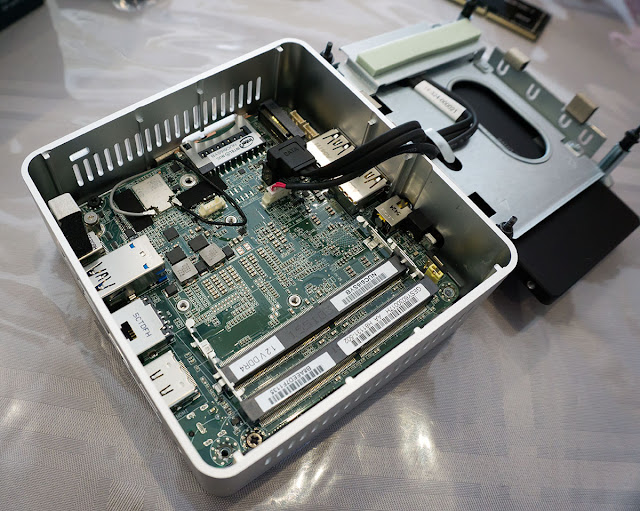 A Taiwanese company has been working on it since 2019
Technology trend 2022: how and why businesses should adopt Cloud Native approach
Digitalization
Apple does this primarily in order to be among the first (or even the first) to release processors according to these standards. Test production of 2-nanometer chips is tentatively scheduled for 2023. The conveyor can operate at full capacity both in the same 2023, and a year or even two later. The exact timing of Apple and TSMC has not yet been specified.
Intel itself also wants to master 2 nanometers. Back in December 2019, she revealed her very ambitious plans to transition to new ultra-modern standards for the production of processors and stay ahead of all her competitors. But, apparently, she still will not be able to overtake TSMC.
Intel is only going to hit 2nm in 2027, plus it has plans for 1.4nm by 2029. In the meantime, back in May 2021, TSMC took a big step towards 1nm.