nVidia GeForce GTX 280 Review
Verdict
Key Specifications
- Review Price: £425.00
The release of the G80 based nVidia GeForce 8800 GTX in November 2006 was, in hindsight, a paradigm shift in the computer graphics world. Not only was it the first DirectX 10 graphics card but it also completely blew away the competition in DirectX 9 games before the arrival of Windows Vista and held this lead for an unprecedented amount of time even when Vista and DirectX 10 did finally arrive. Indeed, not until February of this year, when AMD released the ATI Radeon HD 3870 X2, which used two RV670 cores on one card, did the G80 in its various guises have any real competition.
Not that this competition lasted long. Within a few weeks nVidia released the dual G92 based 9800 GX2, which used a similar two-chips-on-one-card method to the HD 3870 X2, and comfortably regained the top performance crown – at least in the games it worked with. nVidia then followed this up with the 9800 GTX, which used a single G92 based chip to marginally extend nVidia’s performance lead within the single-chip graphics card market. Of course, ATI still had many good cards and it competed very fiercely in the mainstream sub-£150 market but it just couldn’t claim the top spot.
Still, while nVidia held onto its lead with the 9800 series cards, it didn’t really push forward any frontiers. Performance was good but not overwhelming and, while new features like HybridPower are useful, the whole range felt a little disappointing.
Just a few months later, though, nVidia has just launched a brand new graphics processor called GT200 that, at least on paper, looks like it should have all the performance necessary to be a true successor to G80. Made up of 1.4 Billion (yes, that is billion with a ‘B’) transistors, packing in 240 stream processors, 32 ROPs, a 512-bit memory interface, and a whole host of other under-the-bonnet improvements, it is an absolute monster. 2 in size, so 426 dies can be produced per wafer, and you get some idea for just how large and expensive GT200 is.
Two variants on the GT200 will be available at launch, and these will be the first parts to take on nVidia’s revised branding. All the rebranding boils down to is the switching around of letters and numbers so the new cards are called GTX 280 and GTX 260 rather than the x000 GT/GTX/GTS sort of arrangement we’re used to.
The GTX 280 will use the full extent of GT200 with its shader clock running at 1296MHz, 1GB GDDR3 memory running at 1107MHz (2.2GHz effectively), and the rest of the chip purring away at 602MHz. As the power requirement for all this lot will be 236W, the GTX 280 will not only need a conventional six-pin PCI-Express connector but an extra eight-pin one as well.
Meanwhile, the GTX 260, which will be released on the 26th of June (the GTX 280 will be available by the time you read this), has two SM clusters disabled (I’ll explain more about this on the next page) and one ROP partition has also been removed.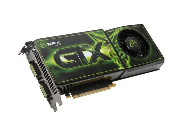 As well as this the clock speeds have been throttled resulting in vital statistics of: 192 shaders running at 1242MHz, 28 ROPs running at 576MHz, and 896MB GDDR3 1000MHz memory. As a result of these speed and component cuts, the GTX 260 will draw less power, 183W to be exact, and consequently needs only a single six-pin PCI-Express power connector.
List pricing is as astronomical as you would expect with the GTX 280 demanding £449 and the GTX 260 £299. What’s more, early indications suggest this pricing won’t be deviated from too much by stores running discounts or trying to out-price each other. Nevermind, hey.
We’ll take a proper look at the GTX260 in a separate article and we’ll have a poke around the physical GTX280 card in a few moments but first let’s look at what makes nVidia’s latest graphical wonder tick.
Although GT200’s architecture is in many ways very similar to that of G80, there is a huge number of tweaks that have been applied to this new core that make it a considerably better whole. Before we get too far into the comparisons, though, let’s get back to basics.
The following is a Streaming Multiprocessor, or SM as nVidia abbreviates it to:
As you can see from the picture, an SM is an array of processing cores called Streaming Processors (SPs), with a portion of cache memory and an instruction scheduler. There’s actually a bit more to it than that, including two Special Function Units (SFU) that aren’t pictured, but we won’t go too far into the specifics. Essentially, this little lot acts like a mini eight core CPU with each core performing the calculations associated with a single pixel. The small (16KB) portion of memory is used to handle only the specific data associated with those eight pixels the SM is currently working on. This is the basic building block of nVidia’s unified shader architecture and is the same on both the G80, G92 and GT200.
(centre)”TPC from GT200”(/centre)
As we zoom out one step we see the first major dividing point between G80/G92 and GT200. In GT200, three of these SMs are combined to form a Texture/Processor Cluster (TPC), whereas G80 and G92 used two SMs per TPC. The principle’s the same, there’s just more in the new chip – 32 SPs vs. 24 on G80.
(centre)”TPC from G80/G92”(/centre)
As well as combining the SMs, a TPC also adds texture processing capabilities and again this is another area where the new chip differs from its forebears, sort of. On G80 you got four texture address units and eight texture filtering units per TPC, with G92 the number of address units doubled to eight while filtering remained at eight units. Now, with GT200 things have, well, stayed the same.
You still get eight texture address units and eight filtering units per TPC, it’s just the ratio of shaders to texturing units has changed. So, while the shader count of each TPC has increased by 50 per cent, the texturing power of each TPC has remained the same. At first this may seem like a backward step but most modern games are becoming shader dependent so the change in ratio makes sense. Moreover, when you look at the bigger picture you’ll see that the total texturing power of GT200 has actually increased a small amount.
What can we say about Counter-Strike: Source that hasn’t been said before? It is simply ”the” benchmark for team-based online shooters and, four years after its release, it’s still one of the most popular game in its genre. In complete contrast to Enemy Territory: Quake Wars, it focuses on small environments and incredibly intensive small-scale battles with one-shot kills the order of the day. If you want to test all elements of your first person shooter skills in one go, this is the game to do it.
We test using the 32-bit version of the game using a custom timedemo taken during a game against bots on the cs_militia map. This has a large amount of foliage, so transparency antialiasing has a significant impact on image quality and performance, and is generally one of the most graphically intensive maps available. We find a framerate of at least 60fps is required for serious gaming as this game relies massively on quick, accurate reactions that simply can’t be compromised by dropped frames.
All in-game settings are set to their maximum and we test with 0xAA 0xAF, 2xAA 4xAF, and 4xAA 8xAA. Transparency anti-aliasing is also manually turned on through the driver, though this is obviously only enabled when normal AA is being used in-game.
Although ATI’s HD 3870 X2 makes a good go of keeping up with GTX280, when it comes to the crunch it simply can’t match nVidia’s latest. Once again, GTX280 reigns supreme.
Call of Duty 4 has to be one of our favourite games of last year. It brought the Call of Duty brand bang up to date and proved that first person shooters didn’t need to have the best graphics, or the longest game time. It was just eight hours of pure adrenaline rush that constantly kept you on edge.
We test using the 32-bit version of the game patched to version 1.4 FRAPS is used to record framerates while we manually walk through a short section of the second level of the game. We find a framerate of 30fps is quite sufficient because, although the atmosphere is intense, the gameplay is less so – it doesn’t hang on quick reactions and high-speed movement.
All in-game settings are set to their maximum and we test with 0xAA and 4xAF. Transparency anti-aliasing is also manually turned on through the driver, though this is obviously only enabled when normal AA is being used in-game.
For some reason this game simply didn’t benefit that much from the various improvements made to GT200 and it is simply trounced by the 9800 GX2. We suspect this is largely due to Call of Duty 4 being a DirectX 9 based game so it is benefiting little from the more DirectX 10 orientated tweaks applied to GT200. It still runs absolutely fine though.
Enemy Territory: Quake Wars distinguishes itself from all our other tests by the fact it uses the open source OpenGL API rather than Microsoft’s DirectX. It’s a team-based first person shooter set in a dystopian future war scenario. As a player you get to choose from an enormous range of character types and playing styles, and there’s a whole host of vehicles to choose from too. Battles can span vast areas of open space and involve a huge number of participants. All in all, it’s multiplayer heaven.
We test using the 32-bit version of the game, which is patched to version 1.4. We use a custom timedemo from the Valley level, which we feel is about as graphically intensive as the game gets. We feel a framerate of at least 50fps is required for this game as the intense multiplayer action and high speed mouse movement demands it.
All in-game settings are set to their maximum and we test with 0xAA 0xAF, 2xAA 4xAF, and 4xAA 8xAA. Transparency anti-aliasing is also manually turned on through the driver, though this is obviously only enabled when normal AA is being used in-game.
The positive story continues with Enemy Territory – GTX280 simply blows away everything else. Even the 9800 GX2 consistently has to play second fiddle and this is a game that scales very well in SLI.
Race Driver: GRID is the newest game in our testing arsenal and it’s currently one of our favourites too.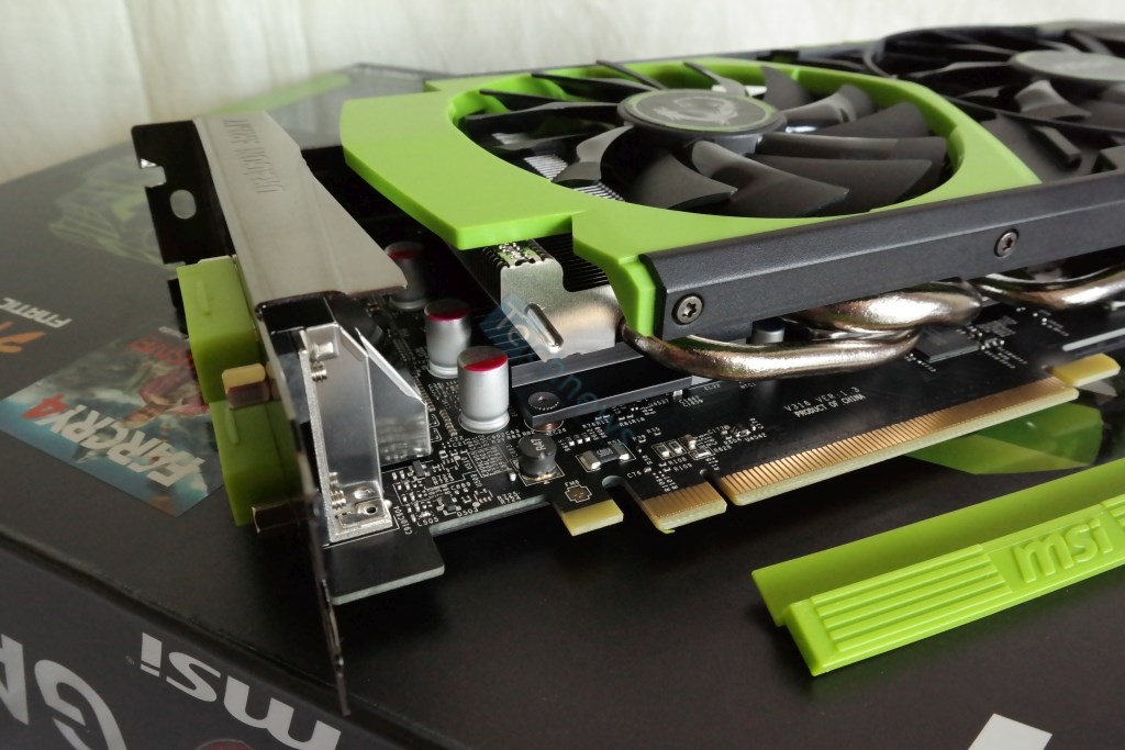 Its combination of arcade style thrills and spills with a healthy dose of realism and extras like Flashback makes it a great pickup and go driving game. It’s also visually stunning with beautifully rendered settings, interactive crowds, destructible environments, and stunning lighting. All that and it’s not the most demanding game on hardware, either.
We test using the 32-bit version of the game, which is unpatched and running in DirectX10 mode. FRAPS is used to record frame rates while we manually complete one circuit of the Okutama Grand Circuit, in a Pro Tuned race on normal difficulty. We find a framerate of at least 40fps is required to play this game satisfactorily as significant stutters can ruin your timing and precision. We’d also consider 4xAA as a minimum as the track, barriers, and car bodies suffer considerably from aliasing and are a constant distraction.
All in-game settings are set to their maximum and we test with 0xAA, 4xAA, and 8xAA. Transparency anti-aliasing is also manually turned on through the driver, though this is obviously only enabled when normal AA is being used in-game.
We had very limited time to test this game so we only got comparable results on a couple of cards. It’s also clear that nVidia hasn’t had a chance to optimise its SLI drivers for this game as the 9800 GX2 struggles more than it should. All told, then, we can’t comment on the big picture. However, even with limited testing it is quite clear that GTX280 is a great choice for playing this game.
While it hasn’t been a huge commercial success and its gameplay is far from revolutionary, the graphical fidelity of Crysis is still second to none and as such it’s still the ultimate test for a graphics card. With masses of dynamic foliage, rolling mountain ranges, bright blue seas, and big explosions, this game has all the eye-candy you could wish for and then some.
We test using the 32-bit version of the game patched to version 1. 1 and running in DirectX 10 mode. We use a custom timedemo that’s taken from the first moments at the start of the game, wondering around the beach. Surprisingly, considering its claustrophobic setting and graphically rich environment, we find that any frame rate above 30fps is about sufficient to play this game.
All in-game settings are set to high for our test runs and we test with both 0xAA and 4xAA. Transparency anti-aliasing is also manually turned on through the driver, though this is obviously only enabled when normal AA is being used in-game.
There’s not much to say here, really. GTX280 is by far the best bet for playing Crysis. In fact, it’s the first card we’ve seen that makes this game playable at 2,560×1,600. This is a great start.
As I alluded to earlier, the GTX280 launch has coincided with a massive push on nVidia’s part to promote GPGPU. However, while this may be interesting it is still far from being of great significance to anyone looking to by one of these cards.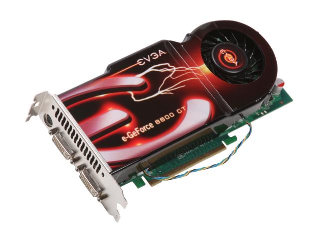 So, until the whole GPGPU spectrum evens out and we get some sort of standards coming into play we will leave analysis of GPGPU performance out of the equation. So, let’s get those games fired up instead.
”’Common System Components”’
* Intel Core 2 Quad QX9770
* Asus P5E3
* 2GB Corsair TWIN3X2048-1333C9 DDR3
* 150GB Western Digital Raptor
* Microsoft Windows Vista Home Premium 32-bit
”’Drivers”’
* GTX280: Forceware 177.34
* Other nVidia cards: Forceware 175.16
* ATI: Catalyst 8.4
”’Cards Tested”’
* nVidia GeForce GTX 280
* nVidia GeForce 9800 GTX
* nVidia GeForce 9800 GX2
* nVidia GeForce 8800 GTX
* nVidia GeForce 8800 GTS 512
* ATI HD 3870 X2
”’Games Tested”’
* Crysis
* Race Driver: GRID
* Enemy Territory: Quake Wars
* Call of Duty 4
* Counter-Strike: Source
The first card we were provided with for review is made by Zotac but apart from the Zotac sticker it is the exact same design as nVidia’s reference board so that’s what we will be basing our assessment on.![]() We will address the specifics of the Zotac board along with a number of other partner cards when we do a roundup soon.
We will address the specifics of the Zotac board along with a number of other partner cards when we do a roundup soon.
The GTX280 card is 267mm long, which is roughly the same length as the 9800 GX2. Also like the GX2, it is completely enclosed by a metal shroud. This protects the delicate electronics from potential damage due to static or general knocks and scrapes and is a development we welcome with open arms.
Again like all nVidia’s recent high-end cards, GTX280 uses a dual-slot heatsink/fan design that employs the slightly off-parallel fan alignment that debuted with the 8800 GTS 512. As we’ve come to expect, the cooler is very effective with it remaining near silent when idle and although it gets loud when under load it is a gentle whoosh rather than a high-pitched squeal or annoying buzz. The card does get very hot and will require a well ventilated case to ensure it doesn’t cause stability problems but, again, this is something we would fully expect from a high-end graphics card.
As mentioned, the peak power draw is a hefty 236W. However, this is a worst case scenario and nVidia has employed some great power saving measures that result in idle power being a mere 25W and power draw during accelerated video playback will only rise to 32W. These are very impressive figures that do make you wonder about the merits of HybridPower, especially as we’ve found the chipsets that support this power saving feature consume significant amounts of power themselves.
Even though the card ”can” draw very little power, it still won’t work without both auxiliary PCI-Express power sockets correctly connected – something that will be made obvious by an LED on the expansion bracket, which glows red if the card hasn’t enough power. nVidia hasn’t gone so far as to use the glowing PCI-Express sockets it used on the GX2 but that was really more of a ”bling” feature than a necessity.
Hidden under rubber flaps along the top of the card are the SLI connectors and an S/PDIF socket. The former enables dual- and triple-SLI configurations and the latter brings the ability to carry digital audio out through the video connections. This supports two-channel LPCM at up to 192KHz, six-channel Dolby Digital at up to 48KHz and DTS 5.1 at up to 96KHz. It doesn’t cover every option, with eight-channel LPCM, Dolby TrueHD and DTS Master Audio being obvious omissions, but it is enough for all but the most elaborate home cinema setups. A DVI-to-HDMI adapter is provided for utilising this.
Outputs are standard fare with two dual-link DVI-I connectors and a seven-pin analogue video connector that supports S-Video natively as well as composite and component via a break-out dongle. Both DVI connections support HDCP encryption so can be used to play back copy-protected HD content like Blu-ray discs.
Video acceleration is the same level as that seen on the 9000-series with H.264, VC-1 and MPEG-2 all benefitting from GPU acceleration. There’s also the questionably useful image post processing, dynamic contrast enhancement, and blue, green and skin tone enhancements that were recently introduced.
One of nVidia’s big marketing campaigns this year has revolved around raising the profile of General Purpose Graphics Processing Unit (GPGPU), the task of performing non-3D-graphics related computation on a GPU. So, with the launch of GT200, nVidia was keen to emphasise the superior GPGPU abilities of its latest chip.
GPUs in general are ideally suited to performing parallel computing tasks, like image manipulation and video conversion, because all those shaders can also be put to task as mini CPUs. Individually they may pale in comparison to a proper CPU but when you’ve got 240 of them, as you have in GT200, the sheer brute force number of shaders will easily out perform any CPU. The big problem at the moment is that writing software to take advantage of parallel processing, and particularly parallel processing on a GPU, is very difficult. This is what prompted nVidia to start working on its CUDA Software Development Kit (SDK), which Hugo recently talked about, and which makes programming for GPGPU considerably easier for the coder.
As well as CUDA as a general programming platform, though, nVidia also recently bought PhysX, the physics processor company, and integrated its technologies into the CUDA SDK. This means that nVidia GPUs can now be put to task in creating life-like physical effects as well as life-like visual effects.
Also, with CUDA being supported by all nVidia’s GPUs since the 8800 GTX, it now has a massive installed user base of 70 million. This has prompted some pretty big name developers to sit up and pay attention to CUDA, including Adobe – it will be using GPU acceleration in its upcoming versions of Photoshop and Premier.
Of course, AMD has also been developing its own competitor to CUDA, in the form of its Close To Metal (CTM) SDK. However, this has had significantly less enthusiastic uptake. Even so, with AMD also planning to support the Havok physics engine and not yet jumping on board with PhysX, the true state of play with regards GPGPU is all very up in the air and personally I’d take the whole thing with a pinch of salt for the time being. That said, for those that are interested, GT200 has made some significant improvements over nVidia’s previous efforts.
Looking at GT200 with regards GPGPU and you have a chip that takes on the following look. The TPCs become mini 24-core processors, each with its own little stores of cache memory. A Thread Scheduler distributes the massive compute load between all the various TPCs and the frame buffer memory acts like main system memory.
Now in its briefings nVidia went into a lot of detail about why GT200 is better than every nVidia GPU that came before when it comes to GPGPU. However, a lot of the improvement is simply down to the basic increase in processing units rather than any grand new designs. The result is an increase from 518 GigaFLOPs of processing power on G80 to 933 GigaFLOPs on GT200.
That said, there are a few architectural improvements as well. First, thread scheduling has been improved to allow dual-issue MAD+MUL functions to be performed more efficiently. Also double precision (64-bit) calculations are now supported though these rely on 30 (one per SM) dedicated double-precision processors rather than using the SPs themselves, resulting in double-precision performance that is one twelfth that of single-precision (32-bit). Four ‘Atomic’ units have also been added. These are designed to handle particular atomic read-modify-write commands with direct access to memory, rather than utilising the chip’s own caches.
All told, though, it’s a lot of stuff that involves very complicated mathematics, and optimisations thereof, and right now little of it is relevant to the general consumer. When mainstream GPGPU applications begin to hit the shelves we’ll come back to these issues and see what difference they really do make.
So, with all that theory out the way, let’s look at the first consumer card based on GT200, the GTX280.
Taking a further step back we a greeted with the following diagram.
Here we see there are ten TPCs making up the shader-power of the chip in a section that nVidia calls the Streaming Processor Array (SPA). In G80 and G92, the SPA consisted of only eight TPCs, which resulted in the total of 128 SPs. With the increase in SPs per TPC and the increase in TPCs per SPA in GT200, we end up with a total 240 SPs – quite some increase, I’m sure you’d agree. This increase in the number of TPCs also accounts for the improvement in texturing power mentioned earlier. With two extra TPCs you get two extra blocks of texturing units, making for a total of 32 texture address units and 32 texture filtering units, up from 24 of each on G92 and 12 addressing units and 24 filtering units on G80.
Above the SPA is the shader-thread dispatch logic, which manages the task of splitting up the huge number of calculations into TPC sized chunks, as well as the raster / setup engine.
Below the SPA are eight ROP partitions, which handle per pixel tasks like anti-aliasing and alpha-blending. Each ROP partition can process four pixels per clock making for a total of 32 pixels per clock for the whole chip. Also, the new ROPs have been tweaked to enable full speed blending (i.e. 32 pixels per clock) – G80 could only blend 12 and output 24 pixels per clock cycle – so antialiasing, particle effects, shadows, and such like should all see a performance increase with GT200. Each ROP has its own little store of L2 cache memory as well as a dedicated 64-bit connection to the frame buffer making for a total memory interface that’s 512-bits wide. Or in other words, colossal!
Elsewhere there have been a number of tweaks applied that include improved geometry shading and Z-occlusion culling performance. Communication between hardware and driver has also been improved reducing potential bottlenecks that could impact performance.
All told, these changes result in some pretty impressive raw performance figures. Over G80, shader processing power has increased by 87.5 per cent, texturing capabilities by 25 per cent, and pixel throughput by 33.3 per cent. Compared to the dual-chip cards that ATI and nVidia both recently introduced, some of the numbers seem less impressive but there are two things to consider here.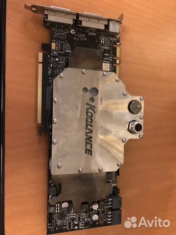 First, figures for the dual card solutions assume a perfect doubling up of performance from the two chips involved, which rarely is the case in real life. Secondly, these dual-chip cards only offer performance increases for the games with which they work properly whereas single chip solutions like GT200 will give you a guaranteed level of performance.
So, that’s the logical picture but how does it all relate to that ginormous chip we saw earlier? Well, take a look below.
This is a picture of the GT200 with the various compute sections highlighted. The unmarked section in the middle performs a variety of roles but primarily it is concerned with managing the rest of the chip so includes things like the thread scheduler and raster setup.
Finally, one note about DirectX10.1. Put simply, GT200 doesn’t support it, which is a shame. Although 10.1 is only a small tweak that doesn’t bring any new features to Microsoft’s gaming API it does improve efficiency, and thus performance, in certain situations. The only thing in nVidia’s favour here is that few developers are yet utilising these new tweaks. However, this won’t be the case forever. We will just have to wait and see how this one pans out.
It’s quite clear that the nVidia GeForce GTX280 performs superbly and, unlike the recent spate of dual-chip cards we’ve seen, this performance is consistent. Ok, it doesn’t absolutely annihilate everything that came before it, like the 8800 GTX did when it arrived, but there’s a large enough step up that those looking to upgrade their 8800 GTXs have a worthwhile option. Especially as more and more game will become dependent on the extra shader hardware that GT200 provides.
We also like the card’s physical layout with the protective covering of the whole card and LEDs to indicate correct power configuration being welcome additions, while the tried and tested black casing, and a great cooler remain from previous cards. Apart from ATI continuing to have the upper hand when it comes to the way audio pass-through is enabled, we really can’t find fault with the GTX280.
One area where the GTX280 inevitably falls down is in its peak power draw but then it’s only as high as we would expect and is still lower than some cards that have come before it. Take into account the incredibly low idle and video decoding power usage, as well as support for HybridPower and you’ve got a card that shouldn’t worry you too much when it comes to your electricity bill.
The only factor that really concerns us is price as nVidia has really put the squeeze on, milking every last drop of profit it can while it still has the performance lead. It’s not a surprising move, and we’re sure its competitors would do the same if they had a chance. However, it’s still lamentable. Moreover, while the GTX280 is undeniably the fastest card around, it isn’t that much faster. Certainly not enough to justify paying twice as much as a 9800 GTX. Indeed, were we to recommend anything right now it would be to go and buy two 9800 GTX cards and run them in SLI (a topic we may cover shortly). Either that or wait for our review of the GTX260 to see how that stacks up.
”’Verdict”’
We can find absolutely no fault in the GTX280 when it comes to performance and it has all the features most gamers should care about. Unfortunately, nVidia has played hard ball with the pricing and we simply can’t recommend buying one at the £400 – £450 asking price.
Score in detail
-
Value 6
-
Features 9
-
Performance 10
GeForce GTX 280 [in 1 benchmark]
NVIDIA
GeForce GTX 280
Buy
- Interface PCIe 2.0 x16
- Core clock speed 602MHz
- Max video memory 1GB
- Memory type GDDR3
- Memory clock speed 1107MHz
- Maximum resolution
Summary
NVIDIA started GeForce GTX 280 sales 16 June 2008 at a recommended price of $649. This is Tesla 2.0 architecture desktop card based on 65 nm manufacturing process and primarily aimed at office use. 1 GB of GDDR3 memory clocked at 1.11 GHz are supplied, and together with 512 Bit memory interface this creates a bandwidth of 141.7 GB/s.
Compatibility-wise, this is dual-slot card attached via PCIe 2.0 x16 interface. Its manufacturer default version has a length of 10.5″ (267 mm) (26.7 cm). 6-pin & 8-pin power connector is required, and power consumption is at 236 Watt.
It provides poor gaming and benchmark performance at
3.56%
of a leader’s which is NVIDIA GeForce RTX 4090.
GeForce GTX
280
vs
GeForce RTX
4090
General info
Of GeForce GTX 280’s architecture, market segment and release date.
| Place in performance rating | 632 | |
| Value for money | 0.45 | |
| Architecture | Tesla 2.0 (2007−2013) | |
| GPU code name | GT200 | |
| Market segment | Desktop | |
| Release date | 16 June 2008 (14 years ago) | |
| Launch price (MSRP) | $649 | |
| Current price | $159 (0.2x MSRP) | of 49999 (A100 SXM4) |
Value for money
To calculate the index we compare the characteristics of graphics cards against their prices.
- 0
- 50
- 100
Technical specs
GeForce GTX 280’s general performance parameters such as number of shaders, GPU base clock, manufacturing process, texturing and calculation speed. These parameters indirectly speak of GeForce GTX 280’s performance, but for precise assessment you have to consider its benchmark and gaming test results.
| Pipelines / CUDA cores | 240 | of 18432 (AD102) |
| CUDA cores | 240 | |
| Core clock speed | 602 MHz | of 2610 (Radeon RX 6500 XT) |
| Number of transistors | 1,400 million | of 14400 (GeForce GTX 1080 SLI Mobile) |
| Manufacturing process technology | 65 nm | of 4 (GeForce RTX 4080 Ti) |
| Thermal design power (TDP) | 236 Watt | of 900 (Tesla S2050) |
| Maximum GPU temperature | 105 °C | |
| Texture fill rate | 48.2 billion/sec | of 939.8 (h200 SXM5) |
| Floating-point performance | 622.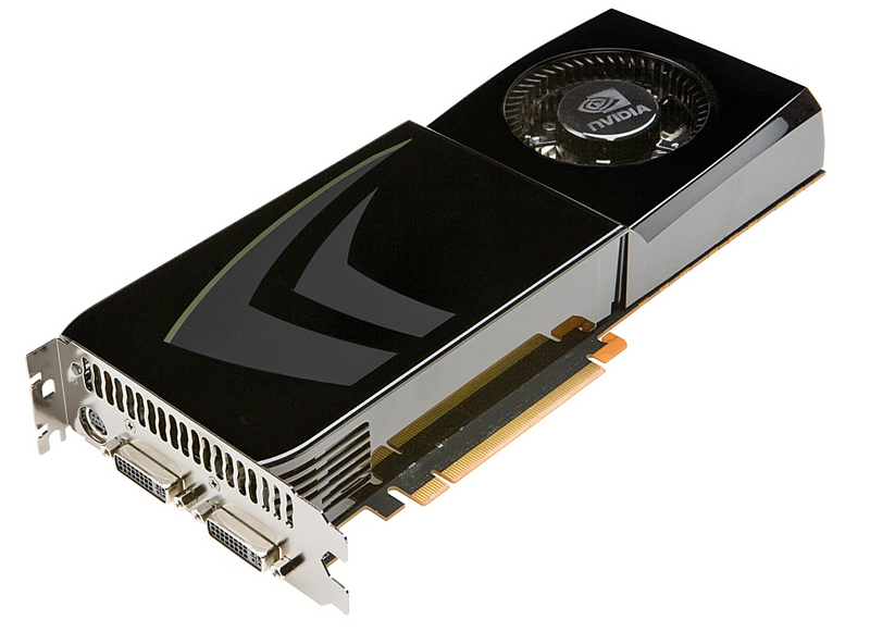 1 gflops 1 gflops |
of 16384 (Radeon Pro Duo) |
Compatibility, dimensions and requirements
Information on GeForce GTX 280’s compatibility with other computer components. Useful when choosing a future computer configuration or upgrading an existing one. For desktop video cards it’s interface and bus (motherboard compatibility), additional power connectors (power supply compatibility).
| Interface | PCIe 2.0 x16 | |
| Length | 10.5″ (267 mm) (26.7 cm) | |
| Height | 4.376″ (111 mm) (11.1 cm) | |
| Width | 2-slot | |
| Supplementary power connectors | 6-pin & 8-pin | |
| SLI options | + |
Memory
Parameters of memory installed on GeForce GTX 280: its type, size, bus, clock and resulting bandwidth. Note that GPUs integrated into processors have no dedicated memory and use a shared part of system RAM instead.
| Memory type | GDDR3 | |
| Maximum RAM amount | 1 GB | of 128 (Radeon Instinct MI250X) |
| Memory bus width | 512 Bit | of 8192 (Radeon Instinct MI250X) |
| Memory clock speed | 1107 MHz | of 21000 (GeForce RTX 3090 Ti) |
| Memory bandwidth | 141.7 GB/s | of 14400 (Radeon R7 M260) |
Video outputs and ports
Types and number of video connectors present on GeForce GTX 280. As a rule, this section is relevant only for desktop reference video cards, since for notebook ones the availability of certain video outputs depends on the laptop model.
| Display Connectors | HDTVDual Link DVI | |
| Multi monitor support | + | |
| Maximum VGA resolution | 2048×1536 | |
| Audio input for HDMI | S/PDIF |
API support
APIs supported by GeForce GTX 280, sometimes including their particular versions.
| DirectX | 11.1 (10_0) | |
| Shader Model | 4.0 | |
| OpenGL | 2.1 | of 4.6 (GeForce GTX 1080 Mobile) |
| OpenCL | 1.1 | |
| Vulkan | N/A | |
| CUDA | + |
Benchmark performance
Non-gaming benchmark performance of GeForce GTX 280. Note that overall benchmark performance is measured in points in 0-100 range.
Overall score
This is our combined benchmark performance rating. We are regularly improving our combining algorithms, but if you find some perceived inconsistencies, feel free to speak up in comments section, we usually fix problems quickly.
GTX 280
3.56
- Passmark
Passmark
This is probably the most ubiquitous benchmark, part of Passmark PerformanceTest suite. It gives the graphics card a thorough evaluation under various load, providing four separate benchmarks for Direct3D versions 9, 10, 11 and 12 (the last being done in 4K resolution if possible), and few more tests engaging DirectCompute capabilities.
Benchmark coverage: 26%
GTX 280
1218
Game benchmarks
Let’s see how good GeForce GTX 280 is for gaming. Particular gaming benchmark results are measured in frames per second. Comparisons with game system requirements are included, but remember that sometimes official requirements may reflect reality inaccurately.
Relative perfomance
Overall GeForce GTX 280 performance compared to nearest competitors among desktop video cards.
AMD Radeon Vega 6
106.46
AMD Radeon HD 6770
101.12
NVIDIA GeForce GTX 260
100
NVIDIA GeForce GTX 280
100
AMD Radeon R9 M270X
98. 88
88
Intel HD Graphics P630
98.31
Intel HD Graphics 630
98.03
AMD equivalent
The nearest GeForce GTX 280’s AMD equivalent is Radeon HD 6770, which is faster by 1% and higher by 1 position in our rating.
Radeon HD
6770
Compare
Here are some closest AMD rivals to GeForce GTX 280:
ATI Radeon HD 4870 X2
107.3
AMD Radeon Vega 6
106.46
AMD Radeon HD 6770
101.12
NVIDIA GeForce GTX 280
100
AMD Radeon R9 M270X
98. 88
88
AMD Radeon HD 7730
97.47
ATI Radeon HD 5750
95.51
Similar GPUs
Here is our recommendation of several graphics cards that are more or less close in performance to the one reviewed.
GeForce GTX
260
Compare
Radeon HD
6770
Compare
GeForce GTX
295
Compare
Radeon HD
5750
Compare
FireStream
9250
Compare
Radeon HD
4850 X2
Compare
Recommended processors
These processors are most commonly used with GeForce GTX 280 according to our statistics.
Core 2
Duo E8400
2.9%
Ryzen 5
3600
2.9%
Core 2
Quad Q9550
2.9%
Core i3
2120
2.5%
Core 2
Quad Q6600
2.5%
Athlon II
X2 250
1.9%
Core i3
2100
1.9%
Core i3
1115G4
1. 6%
6%
Core 2
Quad Q9400
1.3%
Core i3
3220
1.3%
User rating
Here you can see the user rating of the graphics card, as well as rate it yourself.
Questions and comments
Here you can ask a question about GeForce GTX 280, agree or disagree with our judgements, or report an error or mismatch.
Please enable JavaScript to view the comments powered by Disqus.
GT200 Arrives as the GeForce GTX 280 & 260
by Anand Lal Shimpi & Derek Wilsonon June 16, 2008 9:00 AM EST
- Posted in
- GPUs
108 Comments
|
108 Comments
IndexBuilding NVIDIA’s GT200Lots More Compute, a Leetle More TexturingDerek Gets Technical: 15th Century Loom Technology Makes a ComebackTweaks and Enahancements in GT200Derek’s Conjecture Regarding SP Pipelining and TMTNVIDIA’s Dirty Dealing with DX10. 1 and How GT200 Doesn’t Support itGT200 vs. G80: A Clock for Clock ComparisonPower and Power ManagementThe TestCrysisCall of Duty 4Enemy Territory: Quake WarsAssassin’s CreedOblivionThe WitcherBioshockOverclocked: EVGA GeForce GTX 280 FTWSLI Performance Throwdown: GTX 280 SLI vs. 9800 GX2 Quad SLI Finally: GPU Video Encode & Folding@HomeOverclocked and 4GB of GDDR3 per Card: Tesla 10PFinal Words
One-Point-Four-Billion. That’s transistors folks.
The chip is codenamed GT200 and it’s the successor to NVIDIA’s G80 and G92 families. Why the change in naming? The GT stands for «Graphics Tesla» and this is the second generation Graphics Tesla architecture, the first being the G80. The GT200 is launching today in two flavors, the die of the larger one is pictured below:
Um…yeah…we’re reviewing that today
(this die comparison is to scale and that’s a dual-core Penryn)
Let’s put aside all the important considerations for a moment and bask in the glow of sheer geekdom. Intel’s Montecito processor (their dual core Itanium 2) weighs in at over 1.7 billion transistors, but the vast majority of this is L3 cache (over 1.5 billion transistors for 24MB of on die memory). In contrast, the vast majority of the transistors on NVIDIA’s GT200 chip are used for compute power. Whether or not NVIDIA has used these transistors well is certainly the most important consideration for consumers, but there’s no reason we can’t take a second to be in awe of the sheer magnitude of the hardware. This chip is packed full of logic and it is huge.
At most, 94 NVIDIA GT200 die can be produced on a single 300mm 65nm wafer from TSMC. On the other end of the spectrum, Intel can fit around 2500 45nm Atom processors on a 300mm wafer.
If the number of transistors wasn’t enough to turn this thing into a dinner plate sized bit of hardware, the fact that it’s fabbed on a 65nm process definitely puts it over the top. Current CPUs are at 45nm and NVIDIA’s major competitor in the GPU market, AMD, has been building 55nm graphics chips for over 7 months now. With so many transistors, choosing not to shrink their manufacturing process doesn’t seem to make much sense to us. Smaller fab processes offer not only the potential for faster, cooler chips, but also significantly reduce the cost of the GPU itself. Because manufacturing costs are (after ramping production) on a per wafer basis, the more dies that can be packed onto a single waffer, the less each die costs. It is likely that NVIDIA didn’t want to risk any possible delays arising from manufacturing process changes on this cycle, but that seems like a risk that would have been worth taking in this case.
Instead, GT200 is the largest die TSMC has ever fabbed for production. Quite a dubious honor, and I wouldn’t expect NVIDIA to really see this as something of which to be proud. Of course, that doesn’t mean we can’t be impressed with the sheer massiveness of the beast.
And what do we get from all these transistors? Moving up from 690M transistors of the original G80 and 754M transistors in G92 to the 1. 4B transistors of GT200 is not a small tweak. One of the major new features is the ability to processes double precision floating point data in hardware (there are 30 64-bit FP units in GT200). The size of the register file for each SP array has been doubled. The promised ability of an SP to process a MAD and a MUL at the same time has been enhanced to work in more cases (G80 was supposedly able to do this, but the number of cases where it worked as advertised were extremely limited). And the number of SPs has increased from 128 on G80 to 240 with GT200. To better understand what all this means, we’ll take a closer look at the differences between G80 and GT200, but first, the cards.
Clock Speeds, Pricing and HDMI Information
NVIDIA is introducing two GT200 parts today along with slightly tweaked branding. The new brand is called the GeForce GTX, and the first two cards are the GTX 280 and GTX 260.
Gallery: NVIDIA GeForce GTX 280 & 260
Here’s the card, say hello:
The GeForce GTX 280
It’s got a little sibling too:
The GeForce GTX 260
The GeForce GTX 280 features 240 streaming processors running at 1.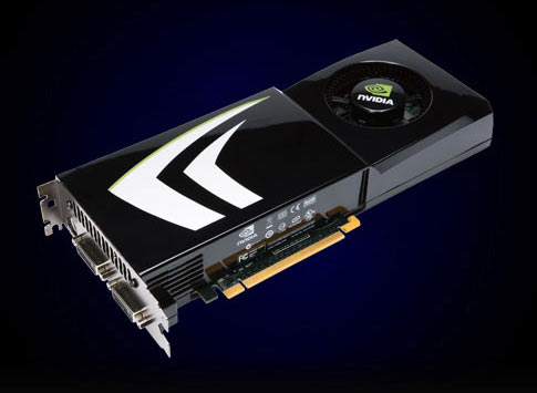 3GHz. It’s got a 512-bit memory interface to 1GB of GDDR3 running at 2.2GHz (1107MHz core clock). The rest of the GPU runs at 602MHz.
| GTX 280 | GTX 260 | 9800 GX2 | 9800 GTX | 8800 GTS 512 | 8800 GT | |
| Stream Processors | 240 | 192 | 256 | 128 | 128 | 112 |
| Texture Address / Filtering | 80 / 80 | 64 / 64 | 128 / 128 | 64 / 64 | 56 / 56 | 56 / 56 |
| ROPs | 32 | 28 | 32 | 16 | 16 | 16 |
| Core Clock | 602MHz | 576MHz | 600MHz | 675MHz | 650MHz | 600MHz |
| Shader Clock | 1296MHz | 1242MHz | 1500MHz | 1690MHz | 1625MHz | 1500MHz |
| Memory Clock | 1107MHz | 999MHz | 1000MHz | 1100MHz | 970MHz | 900MHz |
| Memory Bus Width | 512-bit | 448-bit | 256-bit x 2 | 256-bit | 256-bit | 256-bit |
| Frame Buffer | 1GB | 896MB | 1GB | 512MB | 512MB | 512MB |
| Transistor Count | 1. 4B 4B |
1.4B | 1.5B | 754M | 754M | 754M |
| Manufacturing Process | TSMC 65nm | TSMC 65nm | TSMC 65nm | TSMC 65nm | TSMC 65nm | TSMC 65nm |
| Price Point | $650 | $400 | $500 | $300 | $280 | $170-$230 |
You’ll need a power supply that can deliver up to 236W for the card itself and you’ll need both a 6-pin and an 8-pin PCIe power connector (the board won’t work with two 6-pin connectors).
The GeForce GTX 280 will retail for $650 with availability planned for June 17th.
The GTX 260 brings the total core count down to 192 by disabling two Texture/Processing Clusters on the GPU (but still maintaining more cores than any single-GPU G80/G92 based card). The SPs run slightly slower on the GTX 260 (1242MHz vs. 1296MHz, NVIDIA uses a 27MHz crystal so that’s why we get these funny clock frequencies), while the memory runs at approximately 2GHz (999MHz memory clock, 1998MHz data rate). The GTX 260 also loses one of the 8 64-bit memory controllers, bringing the total memory bus down to 448-bits and total memory size down to 896MB.
The GTX 260 consumes a maximum of 183W and only needs two 6-pin power connectors. The GeForce GTX 260 will set you back $400 and should be available on June 26th.
The GTX 280’s shroud, though it takes some cues from the 9800 GX2, is better engineered to allow for heat expulsion through a larger vent next to the IO ports.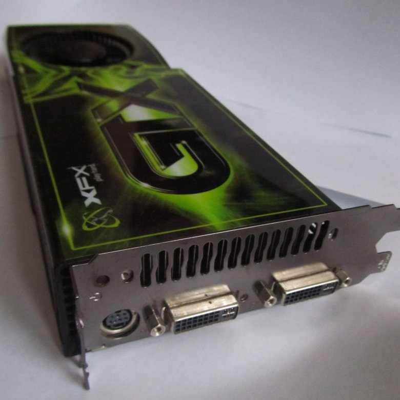 The 9800 GX2 didn’t have a very wide opening to the outside world from which to remove heat. This resulted in the 9800 GX2 disproportionately increasing the heat of the system. Since we run our systems without cases we don’t see problems like this as soon as our readers do, and we would like to thank you for pointing this out to us.
Both the GTX 260 and 280 have two dual-link DVI outputs, which can be converted to HDMI using an adapter if you’d like. You can pass SPDIF using a connector at the top of the card, which will then be passed to the HDMI output when using the DVI-HDMI adapter. For the HTPC enthusiasts out there, the GTX 280 and 260 can output the following audio formats over HDMI:
2-channel LPCM
6-channel DD bitstream
6-channel DTS bitstream
Unfortunately there’s no support for 8-channel LPCM or bitstreaming of Dolby TrueHD or DTS HD-MA.
Building NVIDIA’s GT200
IndexBuilding NVIDIA’s GT200Lots More Compute, a Leetle More TexturingDerek Gets Technical: 15th Century Loom Technology Makes a ComebackTweaks and Enahancements in GT200Derek’s Conjecture Regarding SP Pipelining and TMTNVIDIA’s Dirty Dealing with DX10. 1 and How GT200 Doesn’t Support itGT200 vs. G80: A Clock for Clock ComparisonPower and Power ManagementThe TestCrysisCall of Duty 4Enemy Territory: Quake WarsAssassin’s CreedOblivionThe WitcherBioshockOverclocked: EVGA GeForce GTX 280 FTWSLI Performance Throwdown: GTX 280 SLI vs. 9800 GX2 Quad SLI Finally: GPU Video Encode & Folding@HomeOverclocked and 4GB of GDDR3 per Card: Tesla 10PFinal Words
Tweet
PRINT THIS ARTICLE
Fury XRadeon R9 FuryRadeon R9 NanoRadeon R9 390XRadeon R9 390Radeon R9 380XRadeon R9 380Radeon R7 370Radeon R7 360Radeon R9 295X2Radeon R9 290XRadeon R9 290Radeon R9 280XRadeon R9 285Radeon R9 280Radeon R9 270XRadeon R9 270Radeon R7 265Radeon R7 260XRadeon R7 260Radeon R7 250Radeon R7 240Radeon HD 7970Radeon HD 7950Radeon HD 7870 XTRadeon HD 7870Radeon HD 7850Radeon HD 7790Radeon HD 7770Radeon HD 7750Radeon HD 6990Radeon HD 6970Radeon HD 6950Radeon HD 6930Radeon HD 6870Radeon HD 6850Radeon HD 6790Radeon HD 6770Radeon HD 6750Radeon HD 6670 GDDR5Radeon HD 6670 GDDR3Radeon HD 6570 GDDR5Radeon HD 6570 GDDR3Radeon HD 6450 GDDR5Radeon HD 6450 GDDR3Radeon HD 5570 GDDR5Radeon HD 3750Radeon HD 3730Radeon HD 5970Radeon HD 5870Radeon HD 5850Radeon HD 5830Radeon HD 5770Radeon HD 5750Radeon HD 5670Radeon HD 5570Radeon HD 5550Radeon HD 5450Radeon HD 4890Radeon HD 4870 X2Radeon HD 4870Radeon HD 4860Radeon HD 4850 X2Radeon HD 4850Radeon HD 4830Radeon HD 4790Radeon HD 4770Radeon HD 4730Radeon HD 4670Radeon HD 4650Radeon HD 4550Radeon HD 4350Radeon HD 4350Radeon HD 43500 (IGP 890GX) Radeon HD 4200 (IGP)Radeon HD 3870 X2Radeon HD 3870Radeon HD 3850Radeon HD 3690Radeon HD 3650Radeon HD 3470Radeon HD 3450Radeon HD 3300 (IGP)Radeon HD 3200 (IGP)Radeon HD 3100 (IGP)Radeon HD 2900 XT 1Gb GDDR4Radeon HD 2900 XTRadeon HD 2900 PRORadeon HD 2900 GTRadeon HD 2600 XT DUALRadeon HD 2600 XT GDDR4Radeon HD 2600 XTRadeon HD 2600 PRORadeon HD 2400 XTRadeon HD 2400 PRORadeon HD 2350Radeon X1950 CrossFire EditionRadeon X1950 XTXRadeon X1950 XTRadeon X1950 PRO DUALRadeon X1950 PRORadeon X1950 GTRadeon X1900 CrossFire EditionRadeon X1900 XTXRadeon X1900 XTRadeon X1900 GT Rev2Radeon X1900 GTRadeon X1800 CrossFire EditionRadeon X1800 XT PE 512MBRadeon X1800 XTRadeon X1800 XLRadeon X1800 GTORadeon X1650 XTRadeon X1650 GTRadeon X1650 XL DDR3Radeon X1650 XL DDR2Radeon X1650 PRO on RV530XTRadeon X1650 PRO on RV535XTRadeon X1650Radeon X1600 XTRadeon X1600 PRORadeon X1550 PRORadeon X1550Radeon X1550 LERadeon X1300 XT on RV530ProRadeon X1300 XT on RV535ProRadeon X1300 CERadeon X1300 ProRadeon X1300Radeon X1300 LERadeon X1300 HMRadeon X1050Radeon X850 XT Platinum EditionRadeon X850 XT CrossFire EditionRadeon X850 XT Radeon X850 Pro Radeon X800 XT Platinum EditionRadeon X800 XTRadeon X800 CrossFire EditionRadeon X800 XLRadeon X800 GTO 256MBRadeon X800 GTO 128MBRadeon X800 GTO2 256MBRadeon X800Radeon X800 ProRadeon X800 GT 256MBRadeon X800 GT 128MBRadeon X800 SERadeon X700 XTRadeon X700 ProRadeon X700Radeon X600 XTRadeon X600 ProRadeon X550 XTRadeon X550Radeon X300 SE 128MB HM-256MBR adeon X300 SE 32MB HM-128MBRadeon X300Radeon X300 SERadeon 9800 XTRadeon 9800 PRO /DDR IIRadeon 9800 PRO /DDRRadeon 9800Radeon 9800 SE-256 bitRadeon 9800 SE-128 bitRadeon 9700 PRORadeon 9700Radeon 9600 XTRadeon 9600 PRORadeon 9600Radeon 9600 SERadeon 9600 TXRadeon 9550 XTRadeon 9550Radeon 9550 SERadeon 9500 PRORadeon 9500 /128 MBRadeon 9500 /64 MBRadeon 9250Radeon 9200 PRORadeon 9200Radeon 9200 SERadeon 9000 PRORadeon 9000Radeon 9000 XTRadeon 8500 LE / 9100Radeon 8500Radeon 7500Radeon 7200 Radeon LE Radeon DDR OEM Radeon DDR Radeon SDR Radeon VE / 7000Rage 128 GL Rage 128 VR Rage 128 PRO AFRRage 128 PRORage 1283D Rage ProIntelArc A770 16GBArc A770 8GBArc A750Arc A380Arc A310NVIDIAGeForce RTX 4090GeForce RTX 4080 16GBGeForce RTX 4080 12GBGeForce RTX 3090 TiGeForce RTX 3090GeForce RTX 3080 TiGeForce RTX 3080 12GBGeForce RTX 3080GeForce RTX 3070 TiGeForce RTX 3070GeForce RTX 3060 TiGeForce RTX 3060 rev. 2GeForce RTX 3060GeForce RTX 3050GeForce RTX 2080 TiGeForce RTX 2080 SuperGeForce RTX 2080GeForce RTX 2070 SuperGeForce RTX 2070GeForce RTX 2060 SuperGeForce RTX 2060GeForce GTX 1660 TiGeForce GTX 1660 SuperGeForce GTX 1660GeForce GTX 1650 SuperGeForce GTX 1650 GDDR6GeForce GTX 1650 rev.3GeForce GTX 1650 rev.2GeForce GTX 1650GeForce GTX 1630GeForce GTX 1080 TiGeForce GTX 1080GeForce GTX 1070 TiGeForce GTX 1070GeForce GTX 1060GeForce GTX 1060 3GBGeForce GTX 1050 TiGeForce GTX 1050 3GBGeForce GTX 1050GeForce GT 1030GeForce GTX Titan XGeForce GTX 980 TiGeForce GTX 980GeForce GTX 970GeForce GTX 960GeForce GTX 950GeForce GTX TitanGeForce GTX 780 TiGeForce GTX 780GeForce GTX 770GeForce GTX 760GeForce GTX 750 TiGeForce GTX 750GeForce GT 740GeForce GT 730GeForce GTX 690GeForce GTX 680GeForce GTX 670GeForce GTX 660 TiGeForce GTX 660GeForce GTX 650 Ti BoostGeForce GTX 650 TiGeForce GTX 650GeForce GT 640 rev.2GeForce GT 640GeForce GT 630 rev.2GeForce GT 630GeForce GTX 590GeForce GTX 580GeForce GTX 570GeForce GTX 560 TiGeForce GTX 560GeForce GTX 550 TiGeForce GT 520GeForce GTX 480GeForce GTX 470GeForce GTX 465GeForce GTX 460 SEGeForce GTX 460 1024MBGeForce GTX 460 768MBGeForce GTS 450GeForce GT 440 GDDR5GeForce GT 440 GDDR3GeForce GT 430GeForce GT 420GeForce GTX 295GeForce GTX 285GeForce GTX 280GeForce GTX 275GeForce GTX 260 rev.
 2GeForce GTX 260GeForce GTS 250GeForce GTS 240GeForce GT 240GeForce GT 230GeForce GT 220GeForce 210Geforce 205GeForce GTS 150GeForce GT 130GeForce GT 120GeForce G100GeForce 9800 GTX+GeForce 9800 GTXGeForce 9800 GTSGeForce 9800 GTGeForce 9800 GX2GeForce 9600 GTGeForce 9600 GSO (G94)GeForce 9600 GSOGeForce 9500 GTGeForce 9500 GSGeForce 9400 GTGeForce 9400GeForce 9300GeForce 8800 ULTRAGeForce 8800 GTXGeForce 8800 GTS Rev2GeForce 8800 GTSGeForce 8800 GTGeForce 8800 GS 768MBGeForce 8800 GS 384MBGeForce 8600 GTSGeForce 8600 GTGeForce 8600 GSGeForce 8500 GT DDR3GeForce 8500 GT DDR2GeForce 8400 GSGeForce 8300GeForce 8200GeForce 8100GeForce 7950 GX2GeForce 7950 GTGeForce 7900 GTXGeForce 7900 GTOGeForce 7900 GTGeForce 7900 GSGeForce 7800 GTX 512MBGeForce 7800 GTXGeForce 7800 GTGeForce 7800 GS AGPGeForce 7800 GSGeForce 7600 GT Rev.2GeForce 7600 GTGeForce 7600 GS 256MBGeForce 7600 GS 512MBGeForce 7300 GT Ver2GeForce 7300 GTGeForce 7300 GSGeForce 7300 LEGeForce 7300 SEGeForce 7200 GSGeForce 7100 GS TC 128 (512)GeForce 6800 Ultra 512MBGeForce 6800 UltraGeForce 6800 GT 256MBGeForce 6800 GT 128MBGeForce 6800 GTOGeForce 6800 256MB PCI-EGeForce 6800 128MB PCI-EGeForce 6800 LE PCI-EGeForce 6800 256MB AGPGeForce 6800 128MB AGPGeForce 6800 LE AGPGeForce 6800 GS AGPGeForce 6800 GS PCI-EGeForce 6800 XTGeForce 6600 GT PCI-EGeForce 6600 GT AGPGeForce 6600 DDR2GeForce 6600 PCI-EGeForce 6600 AGPGeForce 6600 LEGeForce 6200 NV43VGeForce 6200GeForce 6200 NV43AGeForce 6500GeForce 6200 TC 64(256)GeForce 6200 TC 32(128)GeForce 6200 TC 16(128)GeForce PCX5950GeForce PCX 5900GeForce PCX 5750GeForce PCX 5550GeForce PCX 5300GeForce PCX 4300GeForce FX 5950 UltraGeForce FX 5900 UltraGeForce FX 5900GeForce FX 5900 ZTGeForce FX 5900 XTGeForce FX 5800 UltraGeForce FX 5800GeForce FX 5700 Ultra /DDR-3GeForce FX 5700 Ultra /DDR-2GeForce FX 5700GeForce FX 5700 LEGeForce FX 5600 Ultra (rev.
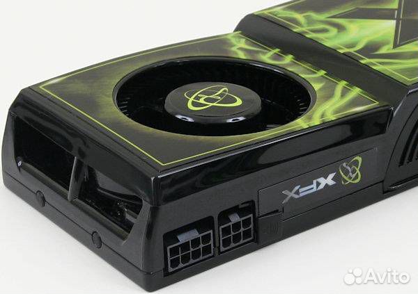 2)GeForce FX 5600 Ultra (rev.1)GeForce FX 5600 XTGeForce FX 5600GeForce FX 5500GeForce FX 5200 UltraGeForce FX 5200GeForce FX 5200 SEGeForce 4 Ti 4800GeForce 4 Ti 4800-SEGeForce 4 Ti 4200-8xGeForce 4 Ti 4600GeForce 4 Ti 4400GeForce 4 Ti 4200GeForce 4 MX 4000GeForce 4 MX 440-8x / 480GeForce 4 MX 460GeForce 4 MX 440GeForce 4 MX 440-SEGeForce 4 MX 420GeForce 3 Ti500GeForce 3 Ti200GeForce 3GeForce 2 Ti VXGeForce 2 TitaniumGeForce 2 UltraGeForce 2 PROGeForce 2 GTSGeForce 2 MX 400GeForce 2 MX 200GeForce 2 MXGeForce 256 DDRGeForce 256Riva TNT 2 UltraRiva TNT 2 PRORiva TNT 2Riva TNT 2 M64Riva TNT 2 Vanta LTRiva TNT 2 VantaRiva TNTRiva 128 ZXRiva 128 9Fury XRadeon R9 FuryRadeon R9 NanoRadeon R9 390XRadeon R9 390Radeon R9 380XRadeon R9 380Radeon R7 370Radeon R7 360Radeon R9 295X2Radeon R9 290XRadeon R9 290Radeon R9 280XRadeon R9 285Radeon R9 280Radeon R9 270XRadeon R9 270Radeon R7 265Radeon R7 260XRadeon R7 260Radeon R7 250Radeon R7 240Radeon HD 7970Radeon HD 7950Radeon HD 7870 XTRadeon HD 7870Radeon HD 7850Radeon HD 7790Radeon HD 7770Radeon HD 7750Radeon HD 6990Radeon HD 6970Radeon HD 6950Radeon HD 6930Radeon HD 6870Radeon HD 6850Radeon HD 6790Radeon HD 6770Radeon HD 6750Radeon HD 6670 GDDR5Radeon HD 6670 GDDR3Radeon HD 6570 GDDR5Radeon HD 6570 GDDR3Radeon HD 6450 GDDR5Radeon HD 6450 GDDR3Radeon HD 5570 GDDR5Radeon HD 3750Radeon HD 3730Radeon HD 5970Radeon HD 5870Radeon HD 5850Radeon HD 5830Radeon HD 5770Radeon HD 5750Radeon HD 5670Radeon HD 5570Radeon HD 5550Radeon HD 5450Radeon HD 4890Radeon HD 4870 X2Radeon HD 4870Radeon HD 4860Radeon HD 4850 X2Radeon HD 4850Radeon HD 4830Radeon HD 4790Radeon HD 4770Radeon HD 4730Radeon HD 4670Radeon HD 4650Radeon HD 4550Radeon HD 4350Radeon HD 4350Radeon HD 43500 (IGP 890GX) Radeon HD 4200 (IGP)Radeon HD 3870 X2Radeon HD 3870Radeon HD 3850Radeon HD 3690Radeon HD 3650Radeon HD 3470Radeon HD 3450Radeon HD 3300 (IGP)Radeon HD 3200 (IGP)Radeon HD 3100 (IGP)Radeon HD 2900 XT 1Gb GDDR4Radeon HD 2900 XTRadeon HD 2900 PRORadeon HD 2900 GTRadeon HD 2600 XT DUALRadeon HD 2600 XT GDDR4Radeon HD 2600 XTRadeon HD 2600 PRORadeon HD 2400 XTRadeon HD 2400 PRORadeon HD 2350Radeon X1950 CrossFire EditionRadeon X1950 XTXRadeon X1950 XTRadeon X1950 PRO DUALRadeon X1950 PRORadeon X1950 GTRadeon X1900 CrossFire EditionRadeon X1900 XTXRadeon X1900 XTRadeon X1900 GT Rev2Radeon X1900 GTRadeon X1800 CrossFire EditionRadeon X1800 XT PE 512MBRadeon X1800 XTRadeon X1800 XLRadeon X1800 GTORadeon X1650 XTRadeon X1650 GTRadeon X1650 XL DDR3Radeon X1650 XL DDR2Radeon X1650 PRO on RV530XTRadeon X1650 PRO on RV535XTRadeon X1650Radeon X1600 XTRadeon X1600 PRORadeon X1550 PRORadeon X1550Radeon X1550 LERadeon X1300 XT on RV530ProRadeon X1300 XT on RV535ProRadeon X1300 CERadeon X1300 ProRadeon X1300Radeon X1300 LERadeon X1300 HMRadeon X1050Radeon X850 XT Platinum EditionRadeon X850 XT CrossFire EditionRadeon X850 XT Radeon X850 Pro Radeon X800 XT Platinum EditionRadeon X800 XTRadeon X800 CrossFire EditionRadeon X800 XLRadeon X800 GTO 256MBRadeon X800 GTO 128MBRadeon X800 GTO2 256MBRadeon X800Radeon X800 ProRadeon X800 GT 256MBRadeon X800 GT 128MBRadeon X800 SERadeon X700 XTRadeon X700 ProRadeon X700Radeon X600 XTRadeon X600 ProRadeon X550 XTRadeon X550Radeon X300 SE 128MB HM-256MBR adeon X300 SE 32MB HM-128MBRadeon X300Radeon X300 SERadeon 9800 XTRadeon 9800 PRO /DDR IIRadeon 9800 PRO /DDRRadeon 9800Radeon 9800 SE-256 bitRadeon 9800 SE-128 bitRadeon 9700 PRORadeon 9700Radeon 9600 XTRadeon 9600 PRORadeon 9600Radeon 9600 SERadeon 9600 TXRadeon 9550 XTRadeon 9550Radeon 9550 SERadeon 9500 PRORadeon 9500 /128 MBRadeon 9500 /64 MBRadeon 9250Radeon 9200 PRORadeon 9200Radeon 9200 SERadeon 9000 PRORadeon 9000Radeon 9000 XTRadeon 8500 LE / 9100Radeon 8500Radeon 7500Radeon 7200 Radeon LE Radeon DDR OEM Radeon DDR Radeon SDR Radeon VE / 7000Rage 128 GL Rage 128 VR Rage 128 PRO AFRRage 128 PRORage 1283D Rage ProIntelArc A770 16GBArc A770 8GBArc A750Arc A380Arc A310NVIDIAGeForce RTX 4090GeForce RTX 4080 16GBGeForce RTX 4080 12GBGeForce RTX 3090 TiGeForce RTX 3090GeForce RTX 3080 TiGeForce RTX 3080 12GBGeForce RTX 3080GeForce RTX 3070 TiGeForce RTX 3070GeForce RTX 3060 TiGeForce RTX 3060 rev.
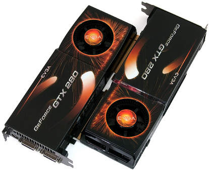 2GeForce RTX 3060GeForce RTX 3050GeForce RTX 2080 TiGeForce RTX 2080 SuperGeForce RTX 2080GeForce RTX 2070 SuperGeForce RTX 2070GeForce RTX 2060 SuperGeForce RTX 2060GeForce GTX 1660 TiGeForce GTX 1660 SuperGeForce GTX 1660GeForce GTX 1650 SuperGeForce GTX 1650 GDDR6GeForce GTX 1650 rev.3GeForce GTX 1650 rev.2GeForce GTX 1650GeForce GTX 1630GeForce GTX 1080 TiGeForce GTX 1080GeForce GTX 1070 TiGeForce GTX 1070GeForce GTX 1060GeForce GTX 1060 3GBGeForce GTX 1050 TiGeForce GTX 1050 3GBGeForce GTX 1050GeForce GT 1030GeForce GTX Titan XGeForce GTX 980 TiGeForce GTX 980GeForce GTX 970GeForce GTX 960GeForce GTX 950GeForce GTX TitanGeForce GTX 780 TiGeForce GTX 780GeForce GTX 770GeForce GTX 760GeForce GTX 750 TiGeForce GTX 750GeForce GT 740GeForce GT 730GeForce GTX 690GeForce GTX 680GeForce GTX 670GeForce GTX 660 TiGeForce GTX 660GeForce GTX 650 Ti BoostGeForce GTX 650 TiGeForce GTX 650GeForce GT 640 rev.2GeForce GT 640GeForce GT 630 rev.2GeForce GT 630GeForce GTX 590GeForce GTX 580GeForce GTX 570GeForce GTX 560 TiGeForce GTX 560GeForce GTX 550 TiGeForce GT 520GeForce GTX 480GeForce GTX 470GeForce GTX 465GeForce GTX 460 SEGeForce GTX 460 1024MBGeForce GTX 460 768MBGeForce GTS 450GeForce GT 440 GDDR5GeForce GT 440 GDDR3GeForce GT 430GeForce GT 420GeForce GTX 295GeForce GTX 285GeForce GTX 280GeForce GTX 275GeForce GTX 260 rev.
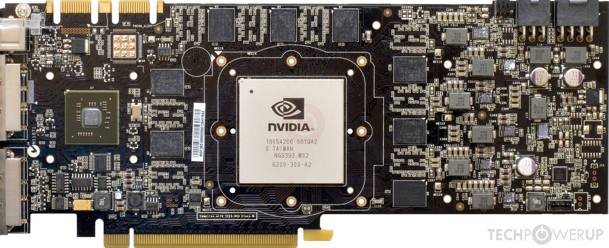 2GeForce GTX 260GeForce GTS 250GeForce GTS 240GeForce GT 240GeForce GT 230GeForce GT 220GeForce 210Geforce 205GeForce GTS 150GeForce GT 130GeForce GT 120GeForce G100GeForce 9800 GTX+GeForce 9800 GTXGeForce 9800 GTSGeForce 9800 GTGeForce 9800 GX2GeForce 9600 GTGeForce 9600 GSO (G94)GeForce 9600 GSOGeForce 9500 GTGeForce 9500 GSGeForce 9400 GTGeForce 9400GeForce 9300GeForce 8800 ULTRAGeForce 8800 GTXGeForce 8800 GTS Rev2GeForce 8800 GTSGeForce 8800 GTGeForce 8800 GS 768MBGeForce 8800 GS 384MBGeForce 8600 GTSGeForce 8600 GTGeForce 8600 GSGeForce 8500 GT DDR3GeForce 8500 GT DDR2GeForce 8400 GSGeForce 8300GeForce 8200GeForce 8100GeForce 7950 GX2GeForce 7950 GTGeForce 7900 GTXGeForce 7900 GTOGeForce 7900 GTGeForce 7900 GSGeForce 7800 GTX 512MBGeForce 7800 GTXGeForce 7800 GTGeForce 7800 GS AGPGeForce 7800 GSGeForce 7600 GT Rev.2GeForce 7600 GTGeForce 7600 GS 256MBGeForce 7600 GS 512MBGeForce 7300 GT Ver2GeForce 7300 GTGeForce 7300 GSGeForce 7300 LEGeForce 7300 SEGeForce 7200 GSGeForce 7100 GS TC 128 (512)GeForce 6800 Ultra 512MBGeForce 6800 UltraGeForce 6800 GT 256MBGeForce 6800 GT 128MBGeForce 6800 GTOGeForce 6800 256MB PCI-EGeForce 6800 128MB PCI-EGeForce 6800 LE PCI-EGeForce 6800 256MB AGPGeForce 6800 128MB AGPGeForce 6800 LE AGPGeForce 6800 GS AGPGeForce 6800 GS PCI-EGeForce 6800 XTGeForce 6600 GT PCI-EGeForce 6600 GT AGPGeForce 6600 DDR2GeForce 6600 PCI-EGeForce 6600 AGPGeForce 6600 LEGeForce 6200 NV43VGeForce 6200GeForce 6200 NV43AGeForce 6500GeForce 6200 TC 64(256)GeForce 6200 TC 32(128)GeForce 6200 TC 16(128)GeForce PCX5950GeForce PCX 5900GeForce PCX 5750GeForce PCX 5550GeForce PCX 5300GeForce PCX 4300GeForce FX 5950 UltraGeForce FX 5900 UltraGeForce FX 5900GeForce FX 5900 ZTGeForce FX 5900 XTGeForce FX 5800 UltraGeForce FX 5800GeForce FX 5700 Ultra /DDR-3GeForce FX 5700 Ultra /DDR-2GeForce FX 5700GeForce FX 5700 LEGeForce FX 5600 Ultra (rev.
 2)GeForce FX 5600 Ultra (rev.1)GeForce FX 5600 XTGeForce FX 5600GeForce FX 5500GeForce FX 5200 UltraGeForce FX 5200GeForce FX 5200 SEGeForce 4 Ti 4800GeForce 4 Ti 4800-SEGeForce 4 Ti 4200-8xGeForce 4 Ti 4600GeForce 4 Ti 4400GeForce 4 Ti 4200GeForce 4 MX 4000GeForce 4 MX 440-8x / 480GeForce 4 MX 460GeForce 4 MX 440GeForce 4 MX 440-SEGeForce 4 MX 420GeForce 3 Ti500GeForce 3 Ti200GeForce 3GeForce 2 Ti VXGeForce 2 TitaniumGeForce 2 UltraGeForce 2 PROGeForce 2 GTSGeForce 2 MX 400GeForce 2 MX 200GeForce 2 MXGeForce 256 DDRGeForce 256Riva TNT 2 UltraRiva TNT 2 PRORiva TNT 2Riva TNT 2 M64Riva TNT 2 Vanta LTRiva TNT 2 VantaRiva TNTRiva 128 ZXRiva 128
You can simultaneously select
up to 10 video cards by holding Ctrl
Reviews of video cards NVIDIA GeForce GTX 280:
-
Testing the ZOTAC GeForce GTX 285 AMP video card! based on 55nm GT200 chip
Zotac GeForce GTX 280 AMP!
-
GeForce GTX 280 versus GeForce 9800 GX2. The fastest modern video cards in comparative testing
XpertVision GeForce GTX 280
NVIDIA GeForce GTX 280 — very fast and super hot / Graphics cards
Authors: Anton Rachko, Vladimir Romanchenko
Today, with an official press release, NVIDIA announced the release of a new generation of GeForce GTX 200 family graphics cards based on the second generation of the unified visual computing architecture — GeForce GTX 280 and GeForce GTX 260. The first sample of a video card based on the GeForce GTX 280 chip has already visited our laboratory , and we are ready to share with our readers the first test results and impressions of the new NVIDIA architecture.
But before moving on to the graphs and conclusions, we bring to your attention a description of the actual architecture of the GeForce GTX 200 family of graphics chips, as well as new and updated NVIDIA technologies and a number of new initiatives, first announced as part of today’s announcement. For those who like to «rewind» the article right away to the conclusions, I would like to emphasize separately: this time NVIDIA announced not only an updated architecture, but also, in a sense, a new philosophy of graphics architecture, with far-reaching consequences.
But first, about the technical features. As a logical development of the GeForce 8 and GeForce 9 series, which represented the first generation of NVIDIA’s unified visual computing architecture, the new GeForce GTX 200 family is based on the second generation of this architecture.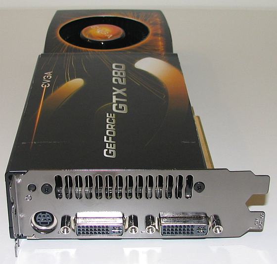
The NVIDIA GeForce GTX 280 and 260 GPUs are the most massive and complex graphics chips known to date — no joke, 1.4 billion transistors each! The most productive solution — GeForce GTX 280, has 240 shader processors, 80 texture processors, supports up to 1 GB of video memory. Detailed specifications of the GeForce GTX 280 and GeForce GTX 260 chips are shown in the table below.
|
NVIDIA GeForce GTX 280 and GTX 260 specifications |
|||||
| Graphics core |
GTX 280 |
65 nm |
1.4 billion |
||
| Graphics clock speed (including dispatcher, texture modules and ROP) |
602 MHz |
576 MHz |
|||
| Processor clock speeds |
1296 MHz |
1242 MHz |
|||
| Number of processor modules |
240 |
192 |
|||
| Memory clock (frequency/data) |
1107 MHz / 2214 MHz |
999 MHz / 1998 MHz |
|||
| Memory interface width |
512 bit |
448 bit |
|||
| Memory bus bandwidth |
141. |
111.9 Gb/s |
|||
| Memory size |
1 GB |
896 MB |
|||
| Number of ROPs |
32 |
28 |
|||
| Number of texture filter modules |
80 |
64 |
|||
| Texture filtering performance |
48.2 Gigatexels/s |
36.9 Gtexels/s |
|||
| HDCP support |
Yes |
||||
| HDMI support |
Yes (DVI to HDMI adapter) |
||||
| Interfaces |
2 x Dual-Link DVI-I |
||||
| RAMDAC, MHz |
400 MHz |
||||
| Tire |
PCI Express 2. |
||||
| Form factor |
Two slots |
||||
| Power connector configuration |
1 x 8-pin |
2 x 6-pin |
|||
| Maximum power consumption |
236 W |
182W |
|||
| GPU Temperature Limit |
105°C |
||||
 7 Gb/s
  0
0
In fact, the modern graphics core of the GeForce GTX 200 family can be imagined as a universal chip that supports two different modes — graphics and computing. Chip architecture of the GeForce 8 and 9 familiesusually represented by arrays of scalable processors (Scalable Processor Array, SPA). The architecture of the GeForce GTX 200 family of chips is based on a revised and improved SPA architecture, consisting of a number of so-called «Texture Processing Clusters» (TPC, Texture Processing Clusters) in graphics mode or «Stream Processing Clusters» in parallel computing mode. Moreover, each TPC module consists of an array of streaming multiprocessors (SM, Streaming Multiprocessors), and each SM contains eight processor cores, also called stream processors (SP, Streaming Processor), or thread processors (TP, Thread Processor). Each SM also includes texture filtering processors for graphics mode, also used for various filtering operations in compute mode.
Below is a block diagram of the GeForce 280 GTX in traditional graphics mode.
By switching to compute mode, the hardware thread manager (above) manages the TPC threads.
Closer look at the TPC cluster: shared memory per SM; each SM processor core can share data among other SM cores via distributed memory, without the need to access an external memory subsystem.
Thus, NVIDIA’s unified shader and computer architecture uses two completely different computational models: for TPC operation, MIMD (multiple instruction, multiple data) is used, for SM computations — SIMT (single instruction, multiple thread), advanced version, SIMD (single instruction, multiple data).
In terms of general characteristics, compared to previous generations of chips, the GeForce GTX 200 family has the following advantages:
- Ability to process three times as many data streams per unit of time
- New command scheduler design with 20% more texture processing efficiency
- 512-bit memory interface (384 bits for the previous generation)
- Optimized z-sampling and compression process for better performance at high screen resolutions
- Architectural enhancements to improve shadow processing performance
- Full-speed frame buffer blending (vs. half-speed on 8800 GTX)
- Doubled instruction buffer for improved computing performance
- Double number of registers for faster calculation of long and complex shaders
- IEEE 754R Double Precision Floating Point Data
- Hardware support for 10-bit color space (DisplayPort only)
Here is a list of the main characteristics of the new chips:
- NVIDIA PhysX support
- Support for Microsoft DirectX 10, Shader Model 4.
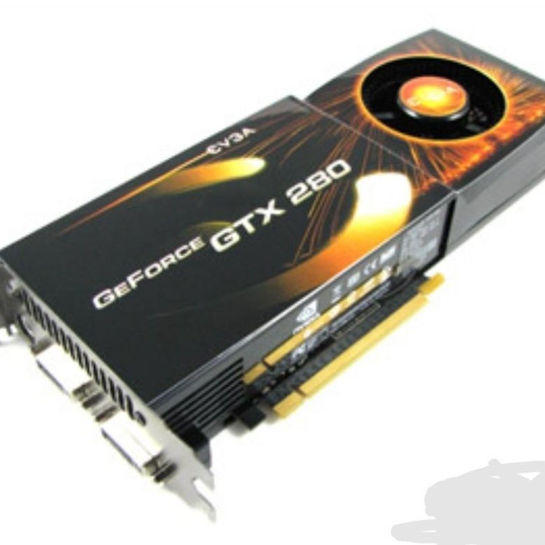 0
0
- Support for NVIDIA CUDA technology
- PCI Express 2.0 bus support
- GigaThread Technology Support
- NVIDIA Lumenex Engine
- 128-bit floating point (HDR)
- OpenGL 2.1 support
- Dual Dual-link DVI support
- Support for NVIDIA PureVideo HD technology
- Support for NVIDIA HybridPower technology
Separately, it is noted that DirectX 10.1 is not supported by the GeForce GTX 200 family. The reason is the fact that when developing chips of a new family, after consultations with partners, it was customary to focus not on supporting DirectX 10.1, which is still in little demand, but on improving the architecture and performance of the chips.
Based on a package of physics algorithms, the implementation of NVIDIA PhysX technology is a powerful real-time physics engine. Currently, PhysX support is implemented in more than 150 games. Combined with a powerful GPU, the PhysX engine provides a significant increase in physical processing power, especially in such areas as creating dust and debris explosions, characters with complex facial expressions, new weapons with fantastic effects, realistically worn or torn fabrics, fog and smoke with dynamic flow around objects.
Another important innovation is the new energy saving modes. Using a precision 65 nm process technology and new circuit solutions, more flexible and dynamic power control has been achieved. Thus, the consumption of the GeForce GTX 200 family of graphics chips in standby mode or in 2D mode is about 25 W; when playing a Blu-ray DVD movie — about 35 W; at full 3D load TDP does not exceed 236 watts. The GeForce GTX 200 graphics chip can be completely disabled due to the support of HybridPower technology with motherboards based on nForce HybridPower chipsets with integrated graphics (for example, nForce 780a or 790i), while the low-intensity graphics stream is simply calculated by the GPU integrated into the motherboard. In addition, GeForce GTX 200 family GPUs also have special power management modules designed to turn off GPU units that are not currently in use.
The user can configure a system based on two or three video cards of the GeForce GTX 200 family in SLI mode when using motherboards based on the corresponding nForce chipsets.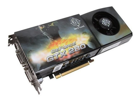 In the traditional Standard SLI mode (with two video cards), approximately 60-90% performance boost in games; in 3-way SLI mode — the maximum number of frames per second at maximum screen resolutions.
The next innovation is support for a new DisplayPort interface with resolutions above 2560 x 1600, with a 10-bit color space (previous generations of GeForce graphics had internal support for 10-bit data processing, but only 8-bit RGB component colors were output).
As part of the announcement of the new GeForce GTX 200 family of GPUs, NVIDIA offers a completely new look at the role of the CPU and GPU in the modern balanced desktop system. Such optimized PC , based on the concept of heterogeneous computing (that is, computing the flow of heterogeneous heterogeneous tasks), according to NVIDIA experts, has a much more balanced architecture and significantly greater computing potential. This refers to the combination of a relatively moderate performance CPU with the most powerful graphics or even SLI system, which allows peak performance in the most demanding games, 3D and media applications.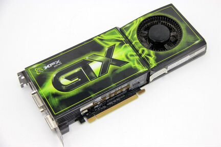
In other words, in short, the concept can be formulated as follows: the central processor in a modern system takes on service functions, while the burden of heavy calculations falls on the graphics system. Approximately the same conclusions (albeit more complex and numerically justified) are observed in a series of our articles devoted to the study of the dependence of performance on the key elements of the system, see the articles Processor dependence of a video system. Part I — Analysis; Processor dependence of the video system. Part II — The impact of CPU cache size and RAM speed; Bot addiction, or why 3D games need a powerful CPU; Processor dependence of the video system. transition area. The «critical» point of the CPU frequency.
However, intensive computing with the help of modern graphics cards is not new for a long time, but it is with the advent of the GeForce GTX 200 family of graphics processors that NVIDIA expects a significant increase in interest in CUDA technology.
CUDA (Compute Unified Device Architecture) is a computing architecture aimed at solving complex problems in consumer, business and technical fields — in any data-intensive applications using NVIDIA GPUs. From the point of view of CUDA technology, the new GeForce GTX 280 graphics chip is nothing more than a powerful multi-core (hundreds of cores!) Processor for parallel computing.
As mentioned above, the graphics core of the GeForce GTX 200 family can be thought of as a chip that supports graphics and computing modes. In one of these modes — «computing», the same GeForce GTX 280 turns into a programmable multiprocessor with 240 cores and 1 GB of dedicated memory — a sort of dedicated supercomputer with teraflop performance, which significantly increases the performance of applications that parallelize data well, for example , video encoding, scientific computing, etc.
GeForce 8 and 9 family graphics processorsbecame the first on the market to support CUDA technology, now they have sold more than 70 million units and interest in the CUDA project is constantly growing. Learn more about the project and download the files you need to get started here. As an example, the screenshots below show examples of computational performance gains obtained by independent users of CUDA technology.
To summarize our brief exploration of the architectural and technological improvements implemented in the new generation of NVIDIA GPUs, let’s highlight the main points. The second generation of the unified visual computing architecture implemented in the GeForce GTX 200 family is a significant step forward compared to the previous generations of GeForce 8 and 9.
Compared to the previous leader GeForce 8800 GTX, the new flagship GeForce GTX 280 has 1.88 times the number of processor cores; capable of processing about 2.5 more threads per chip; has twice the size of file registers and support for double-precision floating-point calculations; supports 1GB memory with 512-bit interface; equipped with a more efficient command dispatcher and improved communication capabilities between chip elements; improved Z-buffer and compression module, support for 10-bit color palette, etc.
For the first time, a new generation of GeForce GTX 200 chips is initially positioned not only as a powerful 3D graphics accelerator, but also as a serious computer solution for parallel computing.
GeForce GTX 280 graphics cards with 1 GB of memory are expected to appear in retail at a price of about $649, new items based on the GeForce GTX 260 with 896 MB of memory — at a price of about $449 (or even $399). It will be possible to check how much the recommended prices match in real retail, it will be possible very soon, because according to all the data, the announcement of the GeForce GTX 200 family is by no means «paper», solutions based on these chips were announced by many NVIDIA partners, and in the very near future new items will appear on the shelves.
Now let’s move on to the description of the first GeForce GTX 280 video card that got into our laboratory, and to the results of its testing.
Authors: Anton Rachko, Vladimir Romanchenko
Video card Leadtek 280GTX
We got the Leadtek 280GTX video card in OEM version, that is, without a box.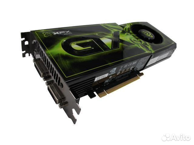 Outwardly, the new product looks like something in between GeForce 9800GTX and GeForce 9800GX2. Both sides of the board are covered with a black casing made of plastic and metal.
The video card package includes:
- power adapter from two 6-pin video card power connectors to one 8-pin; (This is the first time we have encountered such a solution).
- «regular» power adapter for PCI-express video cards;
- DVI to D-sub adapter;
- S-video > S-video + component out adapter;
- CD with drivers;
- Neverwinter Nights 2 CD;
- user manual;
The «double» SLI connector, which allows you to combine 3 video cards, and the S/P-DIF audio signal connector are closed with black plugs. We have already seen a similar solution in the GeForce 9 video card.800GX2, then this approach gave the video card the appearance of a standalone device, something more than just a video card.
The novelty is equipped with two 8 and 6 pin power connectors, which were not closed.
On the opposite side is a 3-Way SLI connector. Two-card configurations use only one of its sub-sockets, while three-card configurations require a special SLI bridge that uses the entire socket.
The Leadtek GTX280 video card is equipped with two DVI connectors and one S-video connector. Not far from the S-video connector is a video card power indicator, which can be very useful in case of power problems, which, by the way, did not bypass us. But more on that later.
The cooling system consists of two parts, a heatsink with a fan and a metal plate that removes heat from the memory chips on the back of the board.
The Leadtek GTX280 video card is very similar to its predecessor GeForce 8800GTX/Ultra.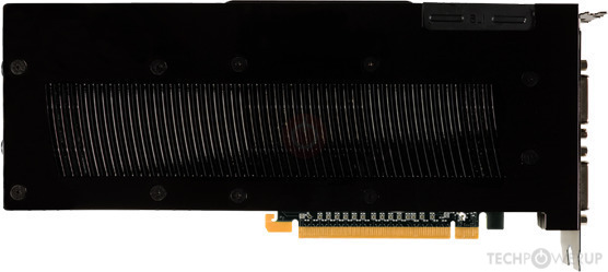 The GT200 graphics chip, like the G80, is equipped with a metal cover that serves to prevent mechanical damage to the crystal. The place for the metal frame around the GPU, like its predecessor, has been preserved, but there is no frame itself. The number of memory chips has increased to 16, which are arranged in 8 pieces on both sides of the board. The memory bus width has increased to 512 bits.
As in the GeForce 8800GTX/Ultra, the developers from NVIDIA used a discrete NVIO chip in the new video card, which is essentially a RAMDAC, which is necessary to support analog displays (D-sub, S-video). At one time, this approach was due to interference from the shader unit of the GPU, as, apparently, now. Interestingly, the G92 chip managed to avoid such a problem. Why NVIDIA engineers did not transfer the experience of designing the G9 chip2 on the GT200 chip, it’s not clear.
The GT200 GPU is massive, with almost a billion and a half transistors hidden under its metal cover.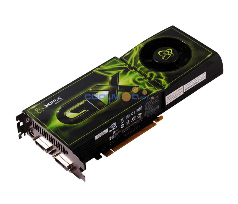 The chip belongs to revision A2.
The memory chips are manufactured by Hynix. The nominal access time of the memory chips is 0.8ns, which corresponds to an effective clock frequency of 2400 MHz.
The cooling system is based on five heat pipes. Three of them distribute heat from the copper base along the aluminum fins, which are blown by a fan on the right, the fourth helps to evenly distribute heat, and the fifth removes heat from the power subsystem to the main radiator.
Authors: Anton Rachko, Vladimir Romanchenko
Efficiency of the cooling system, energy saving system
Riva Tuner 2.09 already supports the new GT200 chip.
Therefore, we did not have any difficulties with measuring the temperature of the video card. We will check the efficiency of the cooling system as before using the Firefly Forest test scene from the 3DMark 06 test suite. The test conditions are 1600×1200 resolution, 4x anti-aliasing and 16x anisotropic filtering. After nine runs of the test, we obtained the following results:
The graphics chip heated up to 85 degrees, while the cooler speed increased from 500 rpm to 1100 rpm. Note that, despite a significant increase in fan speed, the video card cooling system remained very quiet.
The GTX200 series graphics cards boast an efficient power saving system, due to which the graphics card consumes no more than 70 watts of electricity during idle, that is, in 2D mode. This was achieved due to a significant reduction in the clock frequencies of the video card in 2D mode to 300/100 MHz for the GPU and 200 «effective» MHz for the video memory. In 3D mode, the graphics card frequencies increase to 601/1296 MHz for GPU and 2214 «effective» MHz for video memory.
A little earlier, we mentioned possible power problems that we had with this video card, more precisely with the power supply. When launching 3D applications, our video card turned off, and its power indicator changed color from green to red. As it turns out, our Hiper 880W PSU was the culprit. The problem was solved by replacing it with a Thermaltake Toughpower 750W power supply.
Testing, conclusions
We will test the Leadtek GTX280 video card on a test bench with the following configuration:
| Test bench | |
| Processor | Intel Core 2 Quad X6850 3.0 GHz |
| Motherboard | ASUS P5E3 based on Intel X38 |
| RAM | Corsair Dominator DDR3 2 x 2 GB 1333 MHz 6-6-6-18 1T |
| Operating system | Windows XP+SP2+DirectX 9.0c / Windows Vista for DX10 tests |
| Power supply | Thermaltake Toughpower 750W |
For the Leadtek 280GTX video card, we used drivers 177. 34. We will traditionally start reviewing the results with 3DMark tests.
In 3DMark tests, the new product did not show its high-speed potential to the proper extent, yielding to the GeForce 9 video card800GX2. However, all the «i» will dot the game tests that we performed with 4x anti-aliasing and 16x anisotropic filtering.
In the Call of Duty 4 game, the Leadtek 280GTX video card showed slightly better results than the GeForce 9800GX2. The results of other video cards were even less, but, frankly, not so much.
But in the Crysis game, the Leadtek GTX280 video card showed its “teeth” to the rest of the test participants. The GeForce 8800 Ultra is far behind, not to mention the GeForce 8800 GTS 512. The only real opponent for the GeForce 280GTX is the GeForce 9800GX2, but do not forget that the latter is a «glue» of two G92 chips, that is, in fact, these are two video cards in one «bottle».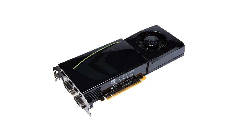
We are finally seeing «playable» values at all three resolutions in Crysis running Windows Vista. The video card GeForce 9800GX2 could not compete with the new product, which was due to the SLI mode. Alas, in the new operating system, this mode has not been brought to perfection.
In the Need for Speed Pro Street Racing game, the first place was taken by the GeForce 9800GX2 video card. So, sometimes the «tops» are still inferior to their predecessors.
In the Call of Juarez game, fortune again turned away from the novelty, and the victory went to the GeForce 9800GX2 video card. However, as we have already said, the latter uses the SLI mode, which imposes some restrictions on it. And these are not only problems in terms of compatibility with some games, which is now extremely rare, but also the ability to display an image on just one monitor and no more.
After switching to Windows Vista, the alignment of forces in the game Call of Juarez hasn’t changed much, the first place belongs to the GeForce 9800GX2 video card.
In Need for Speed Carbon, the Leadtek 280GTX regained its lead. The GeForce 9800GX2 video card is not far behind, but the GT200 chip is still stronger than two G92 chips in SLI mode.
In the Prey game, the Leadtek 280GTX did not lose the lead, but we expected some better results from it. After all, this game is sensitive to the bandwidth of the video memory, which should have increased with the new product due to the expansion of the memory bus to 512 bits.
Terminals
The revolution did not happen, the new GPU GT200 and the video card GeForce 280GTX tested today are a further development of the unified shader architecture from NVIDIA. The new GPU contains more functional blocks than its predecessors, which gives it the right to be called the most powerful GPU to date. It is worth noting that in addition to high performance in 3D applications, the new chip claims to be the first in the field of distributed computing, at the moment it is the Folding@Home project. Do not forget about the computing technology on NVIDIA Cuda GPUs, as well as about the acceleration of «physics» in games. The latter will be fully compatible with the AgeiA PhysX engine, only a special driver is required, which, apparently, is not far away. True, it is still not entirely clear how much the new GT200 chip will be in demand in non-graphical calculations, but we will try to analyze this point in our subsequent articles, when all the necessary drivers and utilities are on hand.
— Discuss the material in the conference
GeForce GTX 280 video card [in 1 benchmark]
NVIDIA
GeForce GTX 280
- PCIe 2.
 0 x16 interface
 - Core clock 602MHz
- Video memory size 1GB
- Memory type GDDR3
- Memory frequency 1107MHz
- Maximum resolution
Description
NVIDIA started GeForce GTX 280 sales on June 16, 2008 at a suggested price of $649. This is a desktop video card based on Tesla 2.0 architecture and 65 nm manufacturing process, primarily designed for office use. It has 1 GB of GDDR3 memory at 1.11 GHz, and coupled with a 512-bit interface, this creates a bandwidth of 141.7 Gb / s.
In terms of compatibility, this is a dual-slot PCIe 2.0 x16 card. The length of the reference version is 26.7 cm. An additional 6-pin & 8-pin power cable is required for connection, and the power consumption is 236 W.
It provides poor performance in tests and games at the level of
3.56%
from the leader, which is NVIDIA GeForce RTX 4090.
GeForce GTX
280
or
GeForce RTX
4090
General information 9999 (A100 SXM4)
Value for money
To obtain an index, we compare the characteristics of video cards and their cost, taking into account the cost of other cards.
- 0
- 50
- 100
Features
GeForce GTX 280’s general performance parameters such as number of shaders, GPU core clock, manufacturing process, texturing and calculation speed. They indirectly speak about GeForce GTX 280’s performance, but for precise assessment you have to consider its benchmark and gaming test results. 939.8 (h200 SXM5)
from 16384 (Radeon Pro Duo)
9595959595959595
Information on GeForce GTX 280 compatibility with other computer components. Useful for example when choosing the configuration of a future computer or to upgrade an existing one. For desktop video cards, these are the interface and connection bus (compatibility with the motherboard), the physical dimensions of the video card (compatibility with the motherboard and case), additional power connectors (compatibility with the power supply).![]()
SLI support
+
RAM
Parameters of memory installed on GeForce GTX 280 — type, size, bus, frequency and bandwidth. For video cards built into the processor that do not have their own memory, a shared part of the RAM is used.
| Memory type | GDDR3 | |
| of 14400 (Radeon R7 M260) |
Video outputs
Types and number of video connectors present on GeForce GTX 280. As a rule, this section is relevant only for desktop reference video cards, since for laptop ones the availability of certain video outputs depends on the laptop model.
| Video connectors | HDTVDual Link DVI | |
| Multi-monitor support |
Benchmark tests
These are the results of GeForce GTX 280 rendering performance tests in non-gaming benchmarks. The overall score is set from 0 to 100, where 100 corresponds to the fastest video card at the moment.
Overall benchmark performance
This is our overall performance rating. We regularly improve our algorithms, but if you find any inconsistencies, feel free to speak up in the comments section, we usually fix problems quickly.
GTX 280
3.56
- Passmark
Passmark
This is a very common benchmark included in the Passmark PerformanceTest package. He gives the card a thorough evaluation, running four separate tests for Direct3D versions 9, 10, 11, and 12 (the latter being done at 4K resolution whenever possible), and a few more tests using DirectCompute.
Benchmark coverage: 26%
GTX 280
1218
Game tests
FPS in popular games on the GeForce GTX 280, as well as compliance with system requirements. Remember that the official requirements of the developers do not always match the data of real tests.
Relative capacity
Overall GeForce GTX 280 performance compared to its nearest desktop competitor.
AMD Radeon Vega 6
106.46
AMD Radeon HD 6770
101.12
NVIDIA GeForce GTX 260
100
NVIDIA GeForce GTX 280
100
AMD Radeon R9 M270X
98.88
Intel HD Graphics P630
98.31
Intel HD Graphics 630
98.03
AMD competitor
We believe that the nearest equivalent to GeForce GTX 280 from AMD is Radeon HD 6770, which is slower by 1% and lower by 1 position in our rating.
Radeon HD
6770
Compare
Here are a few closest competitors to the GeForce GTX 280 from AMD:
ATI Radeon HD 4870 X2
107. 3
AMD Radeon Vega 6
106.46
AMD Radeon HD 6770
101.12
NVIDIA GeForce GTX 280
100
AMD Radeon R9 M270X
98.88
AMD Radeon HD 7730
97.47
ATI Radeon HD 5750
95.51
Other video cards
Here we recommend several video cards that are more or less similar in performance to the reviewed one.
GeForce GTX
260
Compare
Radeon HD
6770
Compare
GeForce GTX
295
Compare
firestream
9250
Compare
Radeon HD
5750
Compare
Radeon HD
4850 X2
Compare
Recommended Processors
According to our statistics, these processors are most often used with the GeForce GTX 280.
Core 2
Duo E8400
2.9%
Ryzen 5
3600
2.9%
Core 2
Quad Q9550
2.9%
Core i3
2120
2.5%
Core 2
Quad Q6600
2.5%
Athlon II
X2 250
1.9%
Core i3
2100
1.9%
Core i3
1115G4
1.6%
Core 2
Quad Q9400
1.3%
Core i3
3220
1.