#2243 (Firewire driver provokes PCI parity error and KDL upon boot (before Tracker loads)) – Haiku
Opened 15 years ago
Closed 8 years ago
| Reported by: | koki | Owned by: | modeenf |
|---|---|---|---|
| Priority: | high | Milestone: | R1 |
| Component: | Drivers/FireWire | Version: | R1/pre-alpha1 |
| Keywords: | Cc: | marcusoverhagen, anevilyak | |
| Blocked By: | Blocking: | ||
| Platform: | All |
Haiku hrev25566 on an HP Pavilion zv5400us laptop.
Haiku KDLs upon boot, after the Deskbar & Terminal are loaded, and before Tracker is run. 100% reproducible.
Haiku will finish to load Tracker and run OK after entering «Continue» command in KDL.
pcistatus/backtraces/listdev outputs and syslog attached.
Attachments
(7)
- pcistatus.jpg
(319.9 KB
) — added by koki 15 years ago. - pcistatus output
- kdl.jpg
(25.8 KB
) — added by koki 15 years ago. - KDL initial screen
- bt.jpg
(194.9 KB
) — added by koki 15 years ago. - Backtrace
- listdev.txt
(3.0 KB
) — added by koki 15 years ago. - listdev output
- syslog.txt
(107.9 KB
) — added by koki 15 years ago. - Syslog
- broken_hardware_patch
(941 bytes
) — added by absabs 15 years ago. - patch3
(2.2 KB
) — added by absabs 15 years ago.
Download all attachments as:
. zip
zip
Show comments
Show property changes
Change History
(34)
by koki, 15 years ago
| Attachment: |
pcistatus.jpg added |
|---|
by koki, 15 years ago
| Attachment: |
kdl.jpg added |
|---|
by koki, 15 years ago
| Attachment: |
bt.jpg added |
|---|
by koki, 15 years ago
| Attachment: |
listdev.txt added |
|---|
by koki, 15 years ago
| Attachment: |
syslog.txt added |
|---|
| Cc: | marcusoverhagen added |
|---|
| Priority: | normal → high |
|---|
by absabs, 15 years ago
| Attachment: |
broken_hardware_patch added |
|---|
| Cc: | anevilyak added |
|---|
| Summary: | KDL upon boot (before Tracker loads) → Firewire driver provokes PCI parity error and KDL upon boot (before Tracker loads) |
|---|
by absabs, 15 years ago
| Attachment: |
patch3 added |
|---|
| Owner: | changed from absabs to modeenf |
|---|---|
| Status: | new → assigned |
| Resolution: | → fixed |
|---|---|
| Status: | assigned → closed |
PCI_X_CAPABILITY (miniport.
 h) — Windows drivers
-
Article -
- 4 minutes to read
The PCI_X_CAPABILITY structure reports the contents of the command and status registers of a device that is compliant with the PCI-X Addendum to the PCI Local Bus Specification.
Syntax
typedef struct {
  PCI_CAPABILITIES_HEADER Header;
  union {
    struct {
      USHORT DataParityErrorRecoveryEnable : 1;
      USHORT EnableRelaxedOrdering : 1;
      USHORT MaxMemoryReadByteCount : 2;
      USHORT MaxOutstandingSplitTransactions : 3;
      USHORT Reserved : 9;
    } bits;
    USHORT AsUSHORT;
  } Command;
  union {
    struct {
      ULONG FunctionNumber : 3;
      ULONG DeviceNumber : 5;
      ULONG BusNumber : 8;
      ULONG Device64Bit : 1;
      ULONG Capable133MHz : 1;
      ULONG SplitCompletionDiscarded : 1;
      ULONG UnexpectedSplitCompletion : 1;
      ULONG DeviceComplexity : 1;
      ULONG DesignedMaxMemoryReadByteCount : 2;
      ULONG DesignedMaxOutstandingSplitTransactions : 3;
      ULONG DesignedMaxCumulativeReadSize : 3;
      ULONG ReceivedSplitCompletionErrorMessage : 1;
      ULONG CapablePCIX266 : 1;
      ULONG CapablePCIX533 : 1;
    } bits;
    ULONG AsULONG;
  } Status;
} PCI_X_CAPABILITY, *PPCI_X_CAPABILITY;
Members
Header
Contains a structure of type PCI_CAPABILITIES_HEADER that identifies the capability and provides a link to the next capability description.
Command
Defines the Command union.
Command.bits
Defines the Command.bits structure.
Command.bits.DataParityErrorRecoveryEnable
Indicates that the data parity error recovery bit is set in the device’s command register, and the device will attempt to recover from data parity errors. For more information about the significance of the value in the parity error recovery bit, see the PCI Local Bus Specification.
Command.bits.EnableRelaxedOrdering
Indicates the enable relaxed ordering bit is set in the device’s command register. This leaves the device free to adopt a more relaxed transaction ordering policy. For more information about how this bit effects transaction ordering, see the PCI Local Bus Specification.
Command.bits.MaxMemoryReadByteCount
Reports the maximum byte count, recorded in the command register, that the device uses when initiating a burst memory read command. For more information about how this bit effects read commands, see the PCI Local Bus Specification.
Command.bits.MaxOutstandingSplitTransactions
Reports the maximum number of split transactions, recorded in the command register, that the device can initiate asynchronously. For more information about how this value effects split transactions, see the PCI Local Bus Specification.
Command.bits.Reserved
Reserved.
Command.AsUSHORT
Reports the data in the device’s command register in the form of a unsigned long integer.
Status
Defines the Status union.
Status.bits
Defines the Status.bits structure.
Status.bits.FunctionNumber
Indicates the value in the function number field of an address of a type 0 configuration transaction. For more information about the meaning of this number, see the PCI Local Bus Specification.
Status.bits.DeviceNumber
Indicates the value in the device number field of the address of a type 0 configuration transaction. For more information about the meaning of this number, see the PCI Local Bus Specification.
Status.bits.BusNumber
Indicates the number of the bus segment on which the device is located. For more information about the meaning of this number, see the PCI Local Bus Specification.
Status.bits.Device64Bit
Indicates when 1 that the bus is 64 bits wide. When 0 the bus is 32 bits wide. For more information about the meaning of the status register’s device 64 bit, see the PCI Local Bus Specification.
Status.bits.Capable133MHz
Indicates when 1 that the device’s maximum operating frequency is 133 MHz. Indicates when 0 that the device’s maximum operating frequency is 66 MHz. For more information about the meaning of status register’s capable 133 Mhz bit, see the PCI Local Bus Specification.
Status.bits.SplitCompletionDiscarded
Indicates when 1 that the device discarded a split completion transaction because the requester rejected it. A value of 0 indicates that the device has not discarded any split completion transactions since the status register’s split completion discarded bit was last cleared. For more information about the status register’s split completion discarded bit, see the PCI Local Bus Specification.
Status.bits.UnexpectedSplitCompletion
Indicates when 1 that the device has received a split completion transaction with the device’s requester ID. Indicates when 0 that the device has not received this kind of transaction. For more information about the meaning of the status register’s unexpected split completion bit, see the PCI Local Bus Specification.
Status.bits.DeviceComplexity
Indicates when 1 that the device is a bridge device. When 0 the device is not a bridge device. For more information about the meaning of the status register’s device complexity bit, see the PCI Local Bus Specification.
Status.bits.DesignedMaxMemoryReadByteCount
Reports the maximum byte count, defined in the status register, that the device uses when it initiates a read sequence. For more information about the meaning of this value, see the PCI Local Bus Specification.
Status.bits.DesignedMaxOutstandingSplitTransactions
Reports the maximum number of split transactions, defined in the status register, that the device can permit at any one time. For more information about the meaning of this value, see the PCI Local Bus Specification.
Status.bits.DesignedMaxCumulativeReadSize
Reports the maximum number of burst memory read transactions, defined in the status register, that the device allows at any one time. For more information about this value, see the PCI Local Bus Specification.
Status.bits.ReceivedSplitCompletionErrorMessage
Indicates when 1 that the device has received a split completion error message. Indicates when 0 that the device has not received a split completion error message.
Status.bits.CapablePCIX266
Defines the ULONG member CapablePCIX266.
Status.bits.CapablePCIX533
Defines the ULONG member CapablePCIX533.
Status.AsULONG
Reports the data in the device’s status register in the form of a unsigned long integer.
Requirements
| Header | miniport.h (include Wdm.h, Miniport.h) |
See also
PCI_CAPABILITIES_HEADER
Transmission plausibility check and error handling
See engine flush oil here. Steering wheel upholstery Primorsky autostudio avant-garde steering wheel upholstery.
To control the reliability of information transfer on the PCI bus, an address and data parity check is used; PCI-X also uses ECC control with single-bit error correction. ECC control is required when operating in Mode 2, it can also be used when operating in Mode 1. The method of plausibility control is reported by the bridge in the initialization template at the end of a bus hardware reset. The bridge chooses the control method that all subscribers of its secondary bus (and itself) support. Errors are reported using the PERR# (protocol signaling between devices) and SERR# (fatal error signal, which usually causes a non-maskable system interrupt) signals.
Parity check uses PAR and PAR64 signals to provide parity for the number of «ones» on the AD[31:0], C/BE[3:0]#, PAR and AD[63:32], C/BE[ 7:4]#, PAR64. The parity signals PAR and PAR64 are generated by the device that currently controls the AD bus (outputs the command and address, attributes or data). Parity signals in PCI mode are generated with a delay of one cycle relative to the AD and C/BE# lines they control. In PCI-X, for read operations, the rules are slightly different: the parity bits in clock N refer to the data bits of clock N — 1 and the C / BE # signals of clock N — 2. The PERR # and SERR # signals are generated by the information receiver in the clock following the clock , in which the parity condition is violated.
In 32-bit ECC mode, the AD[31:0] and C/BE[3:0]# lines are monitored using a 7-bit ECC code with ECC[6:0] signals; 64-bit mode uses 8-bit code with ECC[7:0] signals; in 16-bit mode, a slightly modified ECC7 + 1 scheme is used. In any of the modes, ECC control allows you to correct only single errors and detect most errors with a higher multiplicity. Error correction can be disabled by software (via the ECC control register), and all errors of multiplicity 1, 2 and 3 are detected. In any case, diagnostic information is stored in the ECC control registers. The ECC bits are output to the bus according to the same rules and with the same delays as the parity bits. However, the PERR# and SERR# signals are generated by the information receiver one cycle after the actual ECC bits — the “extra” cycle is given to the analysis of the ECC syndrome and an attempt to correct the error.
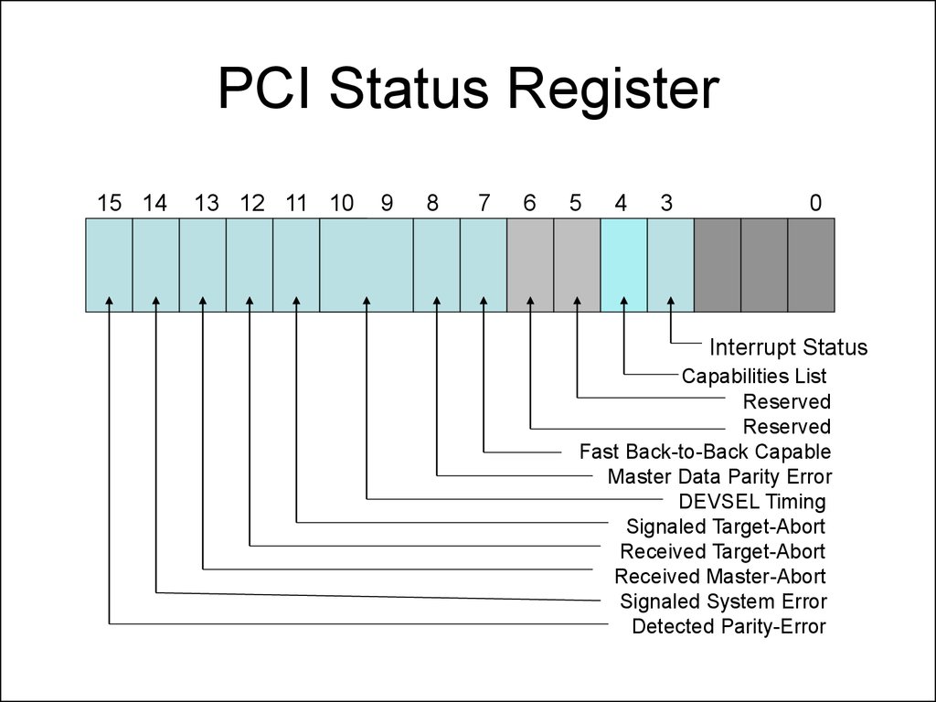
A detected parity error, like an error of more than one bit detected by ECC, is considered unrecoverable. The validity of the information in the address phase, and in the PCI-X and in the attribute phase, is checked by the target device. If an unrecoverable error is detected in these phases, the target device issues a SERR# signal (for one cycle) and sets bit 14 — Signaled System Error in its status register. In the data phase, the device receiving the data validates; if an unrecoverable error is detected, it issues the PERR# signal and sets bit 15 — Detected Parity Error — in its status register.
There is bit 8 (Master Data Parity Error) in the device status register, which indicates the failure of the transaction (sequence) execution due to a detected data error. In PCI and PCI-X, its setting rules are formally different:
- in PCI, this bit is set only by the initiator of the transaction, when he entered (when reading) or detected (when writing) the PERR# signal;
- in PCI-X, this bit is set by the transaction requester or the bridge: as the initiator of read commands, the bridge detects an error in the data; as the initiator of write commands, the bridge detects the PERR# signal; as the target device, the bridge receives a failed completion data or a write transaction failed completion message from one of the devices.

If a data error is detected, the PCI-X device and its driver have two options for behavior:
- without trying to perform any actions to restore and continue operation, set the SERR # signal — this is a catastrophic error signal that can be interpreted by the OS as a reason to reboot. For PCI devices, this is the only possible behavior;
- do not signal SERR#, but try to handle the error yourself. This can only be done programmatically, taking into account all the possible side effects from unnecessary operations (a simple repeated reading can, for example, lead to data loss).
The choice of behavior is provided by setting bit 0 (Uncorrectable Data Error Recovery Enable) in the PCI-X Command register. By default (after a reset), it is set to zero — due to a data error, the SERR# signal is set; another option is to choose a driver that «knows» how to handle errors on its own. Finding an error in the address or attribute phase is always a fatal error.
The initiator (requester) of a transaction must be able to notify the driver that the transaction has been aborted due to the Master Abort (no response from the target device) or Target Abort (failure of the target device) condition, using interrupts or other suitable means. If such notification is not possible, the device shall signal SERR#.
- < back
- Next >
PCI and PCI-X
Protocol, commands and transactions of PCI and PCI-X buses
To control the reliability of information transfer on the PCI bus, the address and data parity check is used; PCI-X also uses ECC control with single-bit error correction. ECC control is required when operating in Mode 2, it can also be used when operating in Mode 1. The method of plausibility control is reported by the bridge in the initialization template at the end of a bus hardware reset. The bridge chooses the control method that all subscribers of its secondary bus (and itself) support. Errors are reported using the PERR# (protocol signaling between devices) and SERR# (fatal error signal, which usually causes a non-maskable system interrupt) signals.
Parity check uses PAR and PAR64 signals to provide parity for the number of «ones» on the AD[31:0], C/BE[3:0]#, PAR and AD[63:32], C/BE[ 7:4]#, PAR64. The parity signals PAR and PAR64 are generated by the device that currently controls the AD bus (outputs the command and address, attributes or data). Parity signals in PCI mode are generated with a delay of one cycle relative to the AD and C/BE# lines they control. In PCI-X, for read operations, the rules are slightly different: the parity bits in clock N refer to the data bits of clock N — 1 and the C / BE # signals of clock N — 2. The PERR # and SERR # signals are generated by the information receiver in the clock following the clock , in which the parity condition is violated.
In 32-bit ECC mode, the AD[31:0] and C/BE[3:0]# lines are monitored using a 7-bit ECC code with ECC[6:0] signals; 64-bit mode uses 8-bit code with ECC[7:0] signals; in 16-bit mode, a slightly modified ECC7 + 1 scheme is used. In any of the modes, ECC control allows you to correct only single errors and detect most errors with a higher multiplicity. Error correction can be disabled by software (via the ECC control register), and all errors of multiplicity 1, 2 and 3 are detected. In any case, diagnostic information is stored in the ECC control registers. The ECC bits are output to the bus according to the same rules and with the same delays as the parity bits. However, the PERR# and SERR# signals are generated by the information receiver one cycle after the actual ECC bits — the “extra” cycle is given to the analysis of the ECC syndrome and an attempt to correct the error.
A detected parity error, like an error of more than one bit detected by ECC, is considered unrecoverable. The validity of the information in the address phase, and in the PCI-X and in the attribute phase, is checked by the target device. If an unrecoverable error is detected in these phases, the target device issues a SERR# signal (for one cycle) and sets bit 14 — Signaled System Error in its status register. In the data phase, the device receiving the data validates; if an unrecoverable error is detected, it issues the PERR# signal and sets bit 15 — Detected Parity Error — in its status register.
There is bit 8 (Master Data Parity Error) in the device status register, which indicates the failure of the transaction (sequence) execution due to a detected data error. In PCI and PCI-X, its setting rules are formally different:
- in PCI, this bit is set only by the initiator of the transaction, when he entered (when reading) or detected (when writing) the PERR# signal;
- in PCI-X, this bit is set by the transaction requester or the bridge: as the initiator of read commands, the bridge detects an error in the data; as the initiator of write commands, the bridge detects the PERR# signal; as the target device, the bridge receives a failed completion data or a write transaction failed completion message from one of the devices.
If a data error is detected, the PCI-X device and its driver have two options for behavior:
- without trying to perform any actions to restore and continue operation, set the SERR # signal — this is a catastrophic error signal that can be interpreted by the OS as a reason to reboot.
 For PCI devices, this is the only possible behavior;
 - do not signal SERR#, but try to handle the error yourself. This can only be done programmatically, taking into account all the possible side effects from unnecessary operations (a simple repeated reading can, for example, lead to data loss).
The choice of behavior is provided by setting bit 0 (Uncorrectable Data Error Recovery Enable) in the PCI-X Command register. By default (after a reset), it is set to zero — due to a data error, the SERR# signal is set; another option is to choose a driver that «knows» how to handle errors on its own. Finding an error in the address or attribute phase is always a fatal error.
The initiator (requester) of a transaction must be able to notify the driver that the transaction has been aborted due to the Master Abort (no response from the target device) or Target Abort (failure of the target device) condition, using interrupts or other suitable means. If such notification is not possible, the device shall signal SERR#.
As mentioned above, the PCI bus does not provide direct memory access using the 8237A-style centralized controller (like the ISA bus). To offload the central processor from routine data transfers, direct bus control is proposed from devices called bus masters (PCI Bus Master). The degree of intelligence of the master device can be different. In its simplest form, the master device transfers blocks of data between the device and system memory (or memory of other devices) as directed by the CPU. Here, the CPU sets the start address, block length, transfer direction, and allows the transfer to start by accessing certain registers of the master device. After that, the transfer is performed when the device is ready (or initiated), without distracting the CPU. This is how direct memory access (DMA) is performed. A more complex DMA controller can organize buffer chaining when reading, scattered writing, etc. — features familiar from the «advanced» DMA controllers for ISA / EISA. A more intelligent master device, usually with its own microcontroller, is not limited to such simple work at the instruction of the CPU — it performs exchanges already according to the program of its controller. Such intelligence is possessed, for example, by USB and IEEE 139 serial bus host controllers.4 discussed in this book.
To make PCI devices compatible with older PC-based software and simplify PCI devices, Intel has developed a special PC/PCI DMA protocol that allows you to centrally emulate a standard (for PC) DMA 8237 controller bundle. An alternative solution is the DDMA mechanism (Distributed DMA — distributed DMA ) allows you to «partition» a standard controller and emulate its individual channels using PCI cards. Both of these mechanisms are implemented only as part of the bridge between the primary PCI bus and the ISA bus, so they may or may not be supported only on the motherboard and enabled in CMOS Setup.
To support the PC/PCI protocol, the main PCI bridge is combined with a DMA controller that is software compatible with the 8237 pair. any of the channels can be connected to the PC/PCI protocol or the LPC bus. The connection of channels to a particular protocol is controlled by a special 16-bit register (offset 90h in the configuration space of the zero function of the ICH device), in which a pair of bits is assigned to each channel. The ICH hub is also the main PCI bridge, naturally providing arbitration functions for bus subscribers, including their own integrated devices. In the PC/PCI protocol, the assignment of a pair of REQi# and GNTi# signals for a pre-selected PCI bus agent, which is a DMA «conductor», is changed. This agent has external (with respect to the PCI bus) pairs of DRQx# and DACKx# signals with logic similar to the ISA DMA signals of the same name, and uses the REQi# and GNTi# lines in the process of requesting bus control in a special way (see the figure below). When an agent receives a DRQx request (one or more), it transmits in serial code the active state of the DRQx request lines on the REQi# line. In the first cycle of CLK, the start bit is transmitted — REQi # low, in the second — request activity DRQ0, then DRQ1 and so on until DRQ7, after which REQ # is kept low. Hub1 will respond to this message via the GNTi# line with a message indicating the channel number, to which a DACKx# confirmation is given for data transmission in subsequent transactions.
Next, the hub (as an initiator on the PCI) organizes data transfer between the PCI DMA agent and the memory, while the transfer direction and the current memory address are controlled by the 8237 controller located in the same hub. During this transmission, the GNTi# signal remains active. The transfer of each byte or word of data is carried out not in one bus cycle, as in ISA DMA, but in a pair of PCI bus cycles: in one cycle, the memory is accessed, in the other, to the PCI DMA agent. The order of the cycles is determined by the direction of transmission (it is clear that data must be read in the first cycle, and written in the second cycle). In these cycles, data is transmitted only on the AD[7:0] lines when working with 8-bit channels and on AD[15:0] when working with 16-bit channels with the corresponding BE[3:0]# signals. In the memory access cycle (Memory Read or Memory Write command), the memory address generated by the corresponding channel 8237 appears. In the I / O cycle (access to the agent), the IO Read or IO Write commands are addressed to special addresses:
- 00h — data transfer;
- 04h — data transfer with end-of-cycle indicator (TC signal of the 8237 controller).
In addition to data transfer, the PC / PCI protocol also allows emulating the DMA verification mode (without data transfer), here the IO Read command with other addresses is used:
- C0h — data verification;
- C4h — Verification of data with the sign of the end of the cycle.
The agent must inform the hub about all changes in the state of the DRQx request lines, including the removal of request signals. If the agent signals the establishment of more than one request line, then after one of them is serviced, the agent must repeat the request for the unserved channel. To send new information about requests, the agent removes the REQi# signal for one cycle and re-introduces the request sending, starting with the start bit. The removal of DRQx corresponding to the currently served channel is signaled by the agent by removing the REQi# signal for two PCI cycles; it must do this 7 cycles before it sends the TRDY# signal in the I / O cycle, otherwise the hub will start the next transmission cycle.