Intel’s Sandy Bridge graphics tech: How good is it?
Sandy Bridge is the culmination of a major Intel design effort to achieve a respectable level of graphics performance and make it a standard feature in all Intel mainstream processors going forward. This week at the Intel Developer Forum in San Francisco, Intel engineers were fairly candid in explaining what Sandy Bridge can and can’t do.
First, some background. A number of technical sessions at IDF were devoted to discussing Sandy Bridge’s graphics technology and the design teams that came together to take this critical feature out of the chipset—a separate companion chip—and put it, for the first time, in the main processor, or CPU.
Intel integrated graphics silicon started appearing in many mainstream laptops about six years ago. And since then has shipped in the lion’s share of PCs sold worldwide. While this has made Intel the leading graphics chip supplier, it has also made it the perennial target of criticism from gaming devotees, who claim—rightfully so in many cases—that Intel graphics fall woefully short in handling a number of mainstream games. In turn, this has led to Intel rebuttals and corresponding primers on Intel integrated graphics.
And Nvidia, a leading graphics chip supplier, has always offered its two cents on Intel’s graphics technology. «Today’s visual computing applications—like photo and video editing, playing games, and browsing the Web—use a GPU for the best experience,» Nvidia said in a statement just prior to IDF. Standalone graphics processing units from Nvidia and Advanced Micro Devices almost invariably offer better performance, particularly on games, but can add cost and, in the case of laptops, can up power consumption requirements.
At IDF, Intel engineers described the markets they can, and cannot, address with Sandy Bridge’s graphics. Sandy Bridge technology will be part of Intel Core i series mobile processors to be introduced into laptops early next year, with the first Sandy Bridge laptop announcements expected at the Consumer Electronics Show in January.
«We’re not trying to target the most high-end discrete (standalone) card. We don’t have the bandwidth, we don’t have the power budget. We’re trying to do the best experience for the mobile platform,» said Opher Kahn, senior principal engineer on the Sandy Bridge design team.
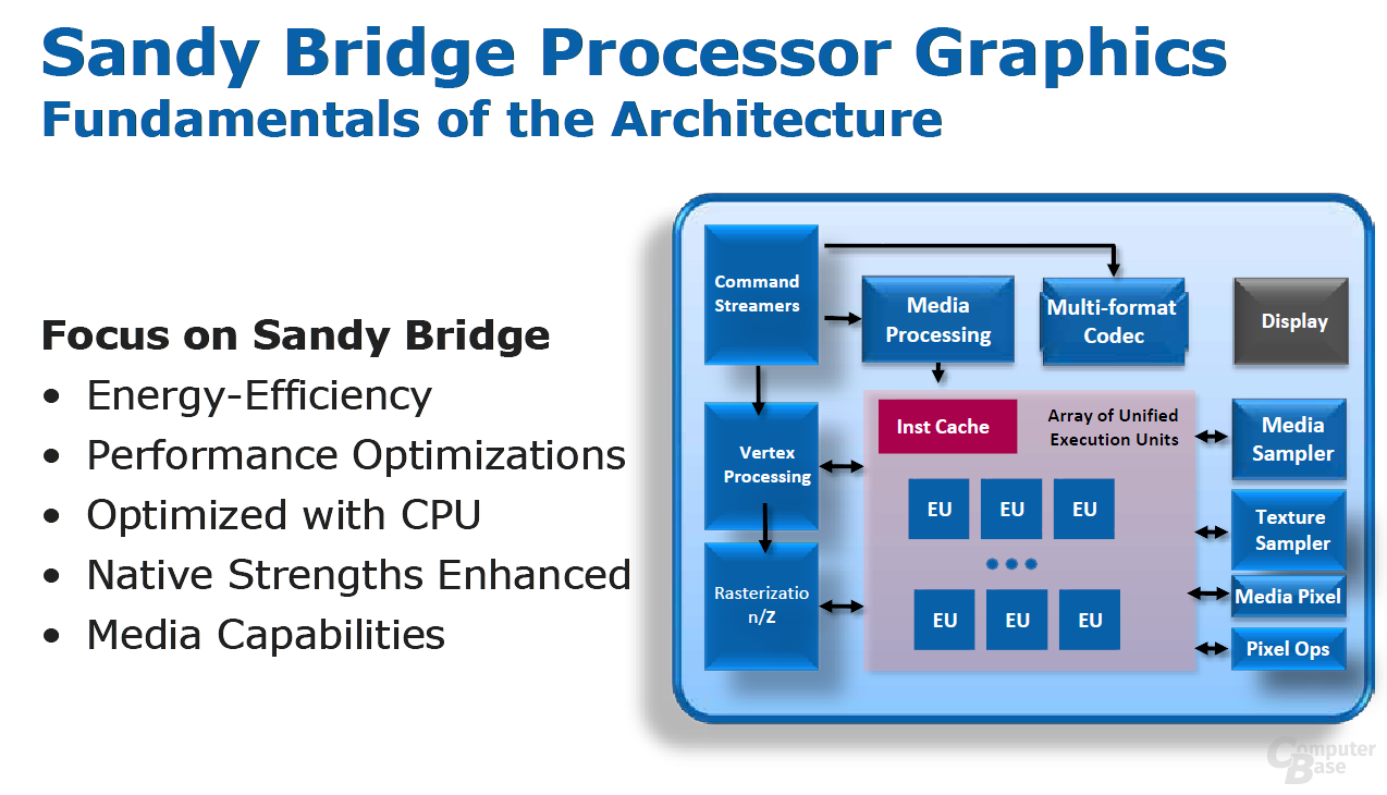
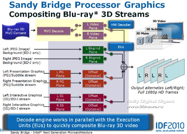
An on-die Sandy Bridge GPU allows it to share high-speed cache memory and improve power efficiency. Intel Better parallelization and better execution units (EU) means better performance for media applications and games. Intel
But can Intel’s Sandy Bridge graphics now handle games? «Historically, Intel has focused their integrated graphics on media capabilities and neglected gaming. With Sandy Bridge, Intel is finally making gaming performance a priority. While the number of shaders (processing units) in Sandy Bridge only increased by 50 percent, they are much more efficient and run at higher frequency so the performance gain is three times or more—putting popular games into reach for many more customers,» said David Kanter, an editor and analyst at Real World Technologies, which covers chip technology in depth.
And Intel addressed this question directly at IDF. «For the games that are designed for the highest-end, extreme edition graphics, the answer is probably no. Unless you run it on a smaller (resolution) screen. For most of the mainstream games, I would expect that the answer is yes,» said Thomas A. Piazza, Intel fellow and director for graphics architecture at the Intel Architecture Group, responding to a question at an IDF technical session.
I also had a chance to chat with Piazza briefly on Tuesday about Sandy Bridge.
Q: What are the main differences between the current Core i series of graphics and Sandy Bridge?
Piazza: On the media side, we moved a lot to fixed function to get a significant performance boost in the same thermal envelope. And on the 3D side, the same thing, the same theme. Actually, the best way to put it is: put a fixed function everywhere that there is no reason to have a soft function. And that’s what gave us the throughput at the power budget.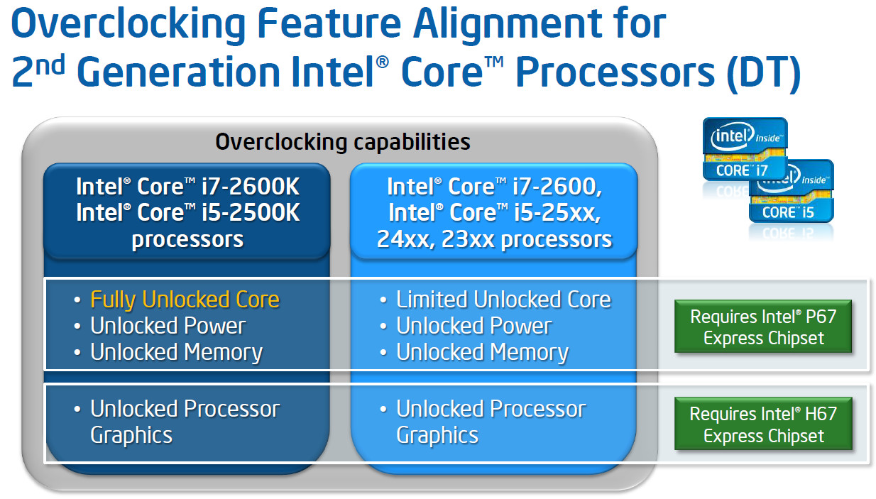 (Note: Fixed function processing is done on the graphics chip, not in «software» on the CPU, increasing performance.)
Q: What is your design constraint versus standalone graphics from Nvidia and AMD? Is it transistors?
Piazza: I don’t think it’s a transistor count thing at all. We’re trying to hit mobile-socketed devices. We’re not going to build a 300-watt graphics device on an integrated CPU. There is no cooling solution for that. We’re talking about the 17-watt socket, the 35-watt socket, the 45-watt socket, and maybe the 55-watt socket. So the cutoff is in the power numbers, it’s not a transistor thing. (Note: 17-watt and 35-watt socket chips typically go into ultrathin and mainstream laptops, respectively. Higher wattage sockets are for bigger system designs.)
Q: Nvidia and ATI boast dozens, if not hundreds of «processing cores.» What is the core count on Sandy Bridge currently?
Piazza: «Twelve (what is also referred to as «shaders»). But I don’t want to say that our twelve is equivalent to their (Nvidia, AMD) twelve. It’s the way we happen to lump things together. If I go out a year, I may have twice as much throughput on one shader.»
Reviews of commercial Sandy Bridge-based laptops will be the final arbiters of performance. And introduction of those systems should peak in the first quarter of 2011.
Intel’s Gen 6 Graphics — The Sandy Bridge Review: Intel Core i7-2600K, i5-2500K and Core i3-2100 Tested
by Anand Lal Shimpion January 3, 2011 12:01 AM EST
- Posted in
- CPUs
- Intel
- Core i5
- Core i7
- Core i3
- Sandy Bridge
283 Comments
|
283 Comments
IntroductionThe LineupOverclocking: Effortless 4.4GHz+ on AirThe 6-series Platform & 6Gbps SATA PerformanceUEFI Support: 3TB Drives & Mouse Support Pre-BootThe Future: Z68 Chipset in Q2, LGA-2011 in Q4A Near-Perfect HTPCIntel’s Quick Sync TechnologyQuick Sync: The Best Way to TranscodeIntel’s Gen 6 GraphicsIntel HD Graphics 2000/3000 PerformanceResolution Scaling with Intel HD Graphics 3000Overclocking Intel’s HD GraphicsThe TestSYSMark 2007 & Photoshop PerformanceVideo Encoding Performance3D Rendering PerformanceFile Compression/Decompression PerformanceVisual Studio 2008, Flash Video Creation, & Excel PerformanceGaming PerformancePower ConsumptionFinal Words
Intel’s Gen 6 Graphics
All 2nd generation Core series processors that fit into an LGA-1155 motherboard will have one of two GPUs integrated on-die: Intel’s HD Graphics 3000 or HD Graphics 2000. Intel’s upcoming Sandy Bridge E for LGA-2011 will not have an on-die GPU. All mobile 2nd generation Core series processors feature HD Graphics 3000.
The 3000 vs. 2000 comparison is pretty simple. The former has 12 cores or EUs as Intel likes to call them, while the latter only has 6. Clock speeds are the same although the higher end parts can turbo up to higher frequencies. Each EU is 128-bits wide, which makes a single EU sound a lot like a single Cayman SP.
Unlike Clarkdale, all versions of HD Graphics on Sandy Bridge support Turbo. Any TDP that is freed up by the CPU running at a lower frequency or having some of its cores shut off can be used by the GPU to turbo up. The default clock speed for both HD 2000 and 3000 on the desktop is 850MHz; however, the GPU can turbo up to 1100MHz in everything but the Core i7-2600/2600K. The top-end Sandy Bridge can run its GPU at up to 1350MHz.
| Processor | Intel HD Graphics | EUs | Quick Sync | Graphics Clock | Graphics Max Turbo |
| Intel Core i7-2600K | 3000 | 12 | Y | 850MHz | 1350MHz |
| Intel Core i7-2600 | 2000 | 6 | Y | 850MHz | 1350MHz |
| Intel Core i5-2500K | 3000 | 12 | Y | 850MHz | 1100MHz |
| Intel Core i5-2500 | 2000 | 6 | Y | 850MHz | 1100MHz |
| Intel Core i5-2400 | 2000 | 6 | Y | 850MHz | 1100MHz |
| Intel Core i5-2300 | 2000 | 6 | Y | 850MHz | 1100MHz |
| Intel Core i3-2120 | 2000 | 6 | Y | 850MHz | 1100MHz |
| Intel Core i3-2100 | 2000 | 6 | Y | 850MHz | 1100MHz |
| Intel Pentium G850 | Intel HD Graphics | 6 | N | 850MHz | 1100MHz |
| Intel Pentium G840 | Intel HD Graphics | 6 | N | 850MHz | 1100MHz |
| Intel Pentium G620 | Intel HD Graphics | 6 | N | 850MHz | 1100MHz |
Mobile is a bit different. The base GPU clock in all mobile SNB chips is 650MHz but the max turbo is higher at 1300MHz. The LV/ULV parts also have different max clocks, which we cover in the mobile article.
As I mentioned before, all mobile 2nd gen Core processors get the 12 EU version—Intel HD Graphics 3000. The desktop side is a bit more confusing. In desktop, the unlocked K-series SKUs get the 3000 GPU while everything else gets the 2000 GPU. That’s right: the SKUs most likely to be paired with discrete graphics are given the most powerful integrated graphics. Of course those users don’t pay any penalty for the beefier on-die GPU; when not in use the GPU is fully power gated.
Despite the odd perk for the K-series SKUs, Intel’s reasoning behind the GPU split does makes sense. The HD Graphics 2000 GPU is faster than any desktop integrated GPU on the market today, and it’s easy to add discrete graphics to a desktop system if the integrated GPU is insufficient. The 3000 is simply another feature to justify the small price adder for K-series buyers.
On the mobile side going entirely with 3000 is simply because of the quality of integrated or low-end graphics in mobile. You can’t easily add in a discrete card so Intel has to put its best foot forward to appease OEMs like Apple. I suspect the top-to-bottom use of HD Graphics 3000 in mobile is directly responsible for Apple using Sandy Bridge without a discrete GPU in its entry level notebooks in early 2011.
I’ve been careful to mention the use of HD Graphics 2000/3000 in 2nd generation Core series CPUs, as Intel will eventually bring Sandy Bridge down to the Pentium brand with the G800 and G600 series processors. These chips will feature a version of HD Graphics 2000 that Intel will simply call HD Graphics. Performance will be similar to the HD Graphics 2000 GPU, however it won’t feature Quick Sync.
Image Quality and Experience
Perhaps the best way to start this section is with a list. Between Jarred and I, these are the games we’ve tested with Intel’s on-die HD 3000 GPU:
Assassin’s Creed
Batman: Arkham Asylum
Borderlands
Battlefield: Bad Company 2
BioShock 2
Call of Duty: Black Ops
Call of Duty: Modern Warfare 2
Chronicles of Riddick: Dark Athena
Civilization V
Crysis: Warhead
Dawn of War II
DiRT 2
Dragon Age Origins
Elder Scrolls IV: Oblivion
Empire: Total War
Far Cry 2
Fallout 3
Fallout: New Vegas
FEAR 2: Project Origin
HAWX
HAWX 2
Left 4 Dead 2
Mafia II
Mass Effect 2
Metro 2033
STALKER: Call of Pripyat
Starcraft II
World of Warcraft
This is over two dozen titles, both old and new, that for the most part worked on Intel’s integrated graphics.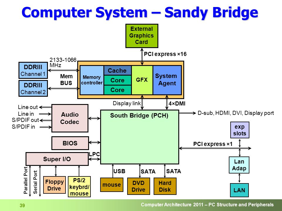 Now for a GPU maker, this is nothing to be proud of, but given Intel’s track record with game compatibility this is a huge step forward.
We did of course run into some issues. Fallout 3 (but not New Vegas) requires a DLL hack to even run on Intel integrated graphics, and we saw some shadow rendering issues in Mafia II, but for the most part the titles—both old and new—worked.
Modern Warfare 2 in High Quality
Now the bad news. Despite huge performance gains and much improved compatibility, even the Intel HD Graphics 3000 requires that you run at fairly low detail settings to get playable frame rates in most of these games. There are a couple of exceptions but for the most part the rule of integrated graphics hasn’t changed: turn everything down before you start playing.
Modern Warfare 2 the way you have to run it on Intel HD Graphics 3000
This reality has been true for more than just Intel integrated graphics however.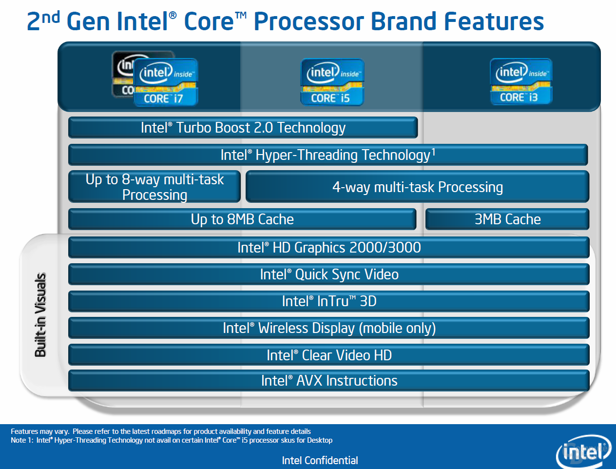 Even IGPs from AMD and NVIDIA had the same limitations, as well as the lowest end discrete cards on the market. The only advantage those solutions had over Intel in the past was performance.
Realistically we need at least another doubling of graphics performance before we can even begin to talk about playing games smoothly at higher quality settings. Interestingly enough, I’ve heard the performance of Intel’s HD Graphics 3000 is roughly equal to the GPU in the Xbox 360 at this point. It only took six years for Intel to get there. If Intel wants to contribute positively to PC gaming, we need to see continued doubling of processor graphics performance for at least the next couple generations. Unfortunately I’m worried that Ivy Bridge won’t bring another doubling as it only adds 4 EUs to the array.
Quick Sync: The Best Way to Transcode
Intel HD Graphics 2000/3000 Performance
IntroductionThe LineupOverclocking: Effortless 4.4GHz+ on AirThe 6-series Platform & 6Gbps SATA PerformanceUEFI Support: 3TB Drives & Mouse Support Pre-BootThe Future: Z68 Chipset in Q2, LGA-2011 in Q4A Near-Perfect HTPCIntel’s Quick Sync TechnologyQuick Sync: The Best Way to TranscodeIntel’s Gen 6 GraphicsIntel HD Graphics 2000/3000 PerformanceResolution Scaling with Intel HD Graphics 3000Overclocking Intel’s HD GraphicsThe TestSYSMark 2007 & Photoshop PerformanceVideo Encoding Performance3D Rendering PerformanceFile Compression/Decompression PerformanceVisual Studio 2008, Flash Video Creation, & Excel PerformanceGaming PerformancePower ConsumptionFinal Words
PRINT THIS ARTICLE
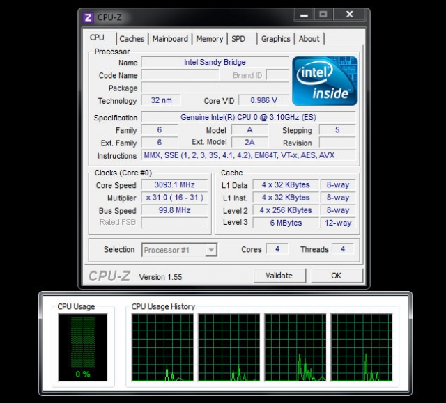
New Intel Sandy Bridge architecture processors
Processors of the new
Sandy architecture
Bridge
(«sand bridge») replaced the current
Nehalem
(45 nm) and Westmere
(32 nm). Under the release rule
tick-tock, Sandy
Bridge
is «such» — a new microarchitecture,
released on an already developed technical process
(32 nm). However, at the end of 2011
another tick is expected — a little
updated 22nm version of Sandy
Bridge
called Ivy
Bridge
(ivy bridge).
Short list
real advantages compared to
current generation of Intel CPU:
-
Into the chip now
chipset northbridge integrated together
with video core. -
Self graphic
core (GPU) updated but kept
Possibility to connect external
graphics. -
The core of the common
destinations support expansion
AVX (Advanced)
Vector
extensions).
Being an evolutionary development of a set
SSE commands, this innovation will allow
improve processor performance
at the same clock frequency. Besides,
new processors will inherit the mechanism
support for AES encryption, for the first time
implemented in Westmere.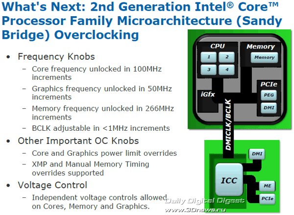
-
L3 cache increased
throughput through
high-speed connection to cores
(including to the GPU). -
Technology
auto-acceleration TurboBoost
improved and now allows automatically
raise/lower x86 core frequencies and
graphics, and even higher level
nominal heat pack (TDP), if
general temperature conditions are
allow. There was also an additional
technology within Turbo
boost,
which for maximum responsiveness
systems in interactive tasks can
for a short time, but very aggressively
increase the frequency of the processor.
Here on these and more
small points and go through.
TO
large-block
the CPU core has not changed. It’s all about the details.
IN
O
front, the main innovation is the cache on
1536 uops buffering results
decoder work. Also redesigned
branch predictor storing
now twice as many target addresses and
a longer history of command behavior.
Connected to it is a block that defines
hits in the mop-cache, and in these cases
L1I cache, length predecoder and decoders
turn off to save energy. Also
performance increases for
by improving the response to incorrect
predicted transition (correct branch
may end up in the mop cache) and release
from having to decode long
commands for several cycles at each
their performance.
Rear of the conveyor
changed more. First obvious change:
transition from the full ROB buffer (storing
mops and the values of the registers they change)
to a combination of abbreviated ROB (storing
only mops in original order) and
two physical register files
(PRFs that store the contents of the renamed
registers that uops refer to)
– integer and vector-real.
The meaning of the transition is that instead of forwarding
mops are sent along with the data
only links to registers, and mops themselves
and the data stays in place until
resignations — as a result of the removal
unnecessary transfers saves energy.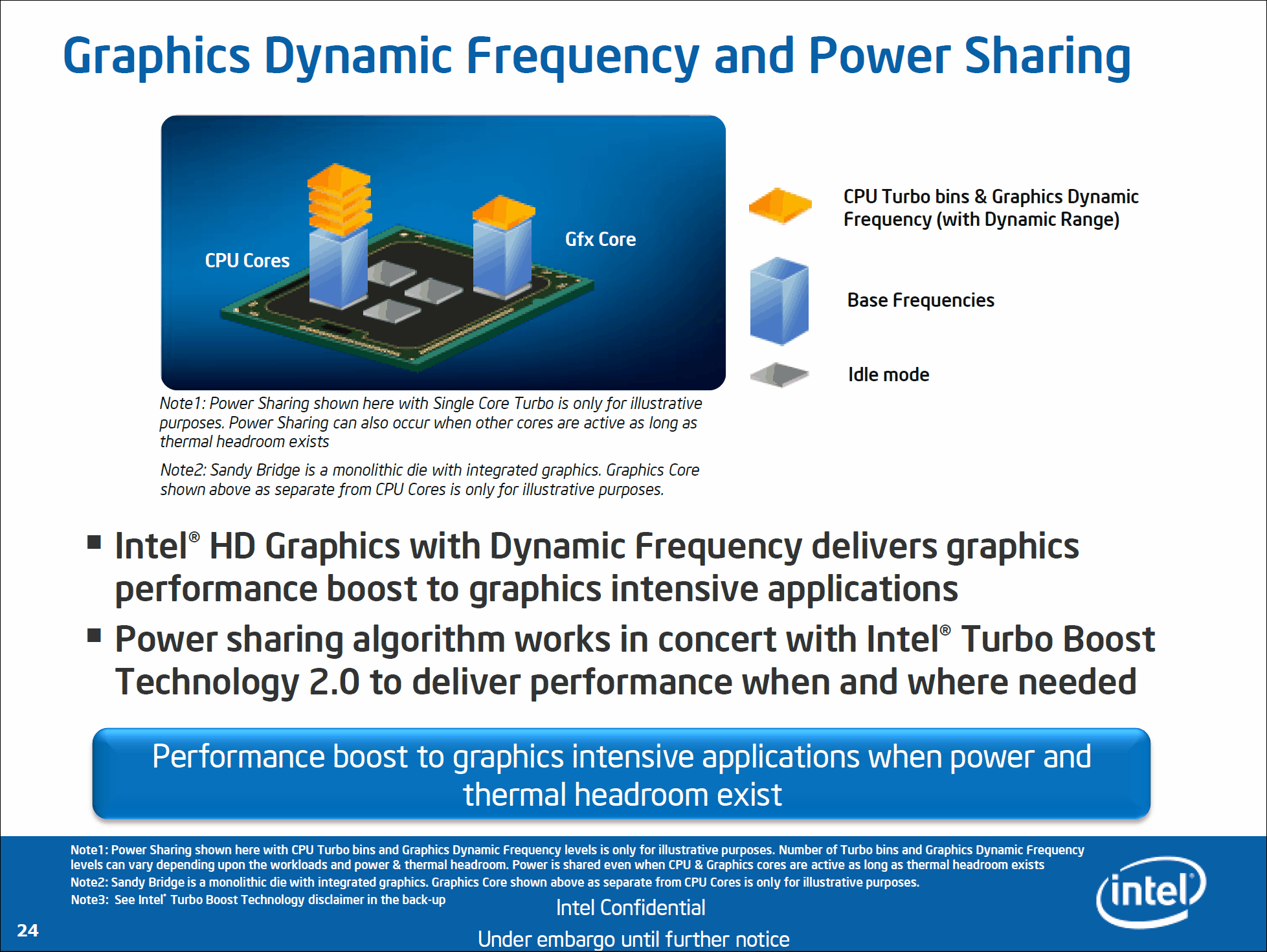
Responsible for performance
duty increase in the size of everything
variety of buffers and queues.
H
A
functional unit level main
news — support for AVX, a new addition
x86-64 command systems. Unlike the next
SSE just adding new commands,
AVX allows:
-
refers to
256-bit ymm vector registers,
extending the usual xmm for SSE; -
use during
all vector commands 3-4 operands in
non-destructive form when the result
operation does not destroy the original
arguments; -
save on
size of vector instructions due to
code compaction (especially for SSSE3 and
Further).
R
of course
there are also new instructions — for the distribution
elements in vector and masked
memory operations.
To good
beginnings did not remain only at the level
AVX command recognition, FU block redesigned
to handle ymm registers with the same
speed, like xmm.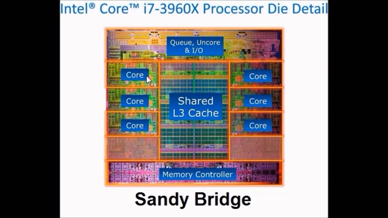 For this 128-bit
adder, multiplier, ALU and shufflers
doubled the bit depth, respectively
boosting peak performance
kernels.
L1D cache increased by 50%
full bandwidth — now
that’s 32 bytes of read + 16 bytes of write per
tact. To do this, in LSU (L1D controller)
a second 16-byte read port is supplied.
This will allow you to saturate at the right pace.
FU data when executing AVX code.
Out of the core (so
Intel
names the rest of the CPU not included
in general purpose kernels) list of changes
opens, as it were, a new (appeared yet
in March 2010 in 8-core server chips
Nehalem EX)
32-byte ring bus linking
L3 cache, compute and graphics
nuclei and «system agent» (former northern
bridge with ICP for DDR3 memory). L3 Cache,
designated as LLC (last
level
cache,
last level cache), consists of
several banks (according to the number of cores of the total
destination) with an access port in each.
The ring bus that connects it all
operates at a frequency comparable to the frequency
cores, and ideally transmits
the amount of data equal to the product
32 for the number of banks.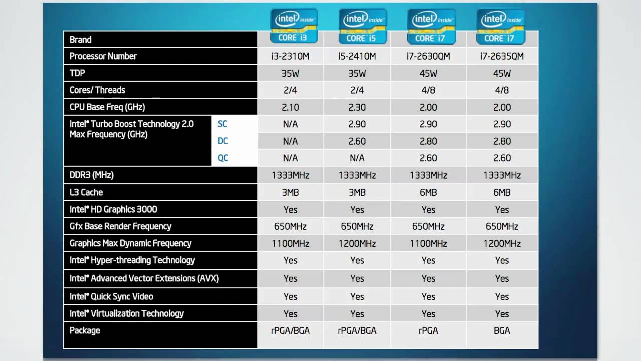 In this manner
shared L3 performance
Cache
increases in proportion to the number
cores, but the promised reduction in latency
(at least in cycles) doubtful
compared to centralized
controller L3.
Sandy
Bridge
is the first architecture
integrates on a single chip as a CPU,
as well as the GPU. chips
with Sandy architecture
Bridge
will be produced according to the standards of 32 nm
technology, however, unlike
existing analogues, integrated
the graphics core will be created in them
according to the same 32 nm standards and will be located on
one chip with computing
cores.
These two components
can share a common Cache
— memory integrated on a chip,
which improves overall work efficiency
systems thanks to the superiority of Cache
over RAM (Intel
speaks of a fourfold increase
throughput efficiency).
Since the GPU is now located on
processor chip, and not on a separate one,
as in current Core i3/i5, L3 Cache
can be used incl. and for
graphics, which alleviates the disadvantage
system memory bandwidth
compared to specialized
video memory, rarely available for
built-in GPU.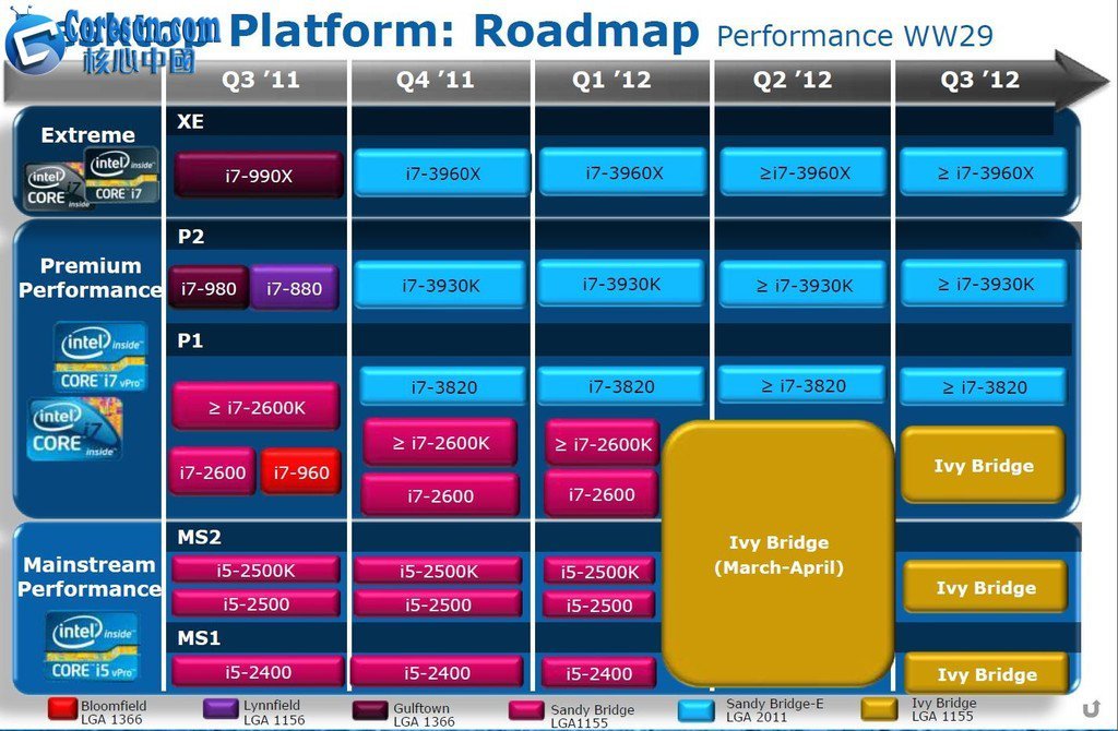
The video core is promised
double performance, and
only due to the fast L3 Cache,
but also from doubling the number of executive
blocks up to 12 — however, not in all models.
Support for DirectX 10 has also been introduced (and on
yard is already the 11th…) and new HD-video formats
for energy efficient hardware
speed up (de)coding.
The CPU will receive
triple power — for common cores
destination and L3, for the GPU, as well as for
system agent with controllers
all kinds of tires.
Controller
thermal mode and power implements
updated version of TurboBoost technology,
taking into account transient processes. She
allow in a short time
(20–60 sec) overclock cores (including GPU) to
frequencies at which heat generation even
above the nominal peak (TDP), if before
The CPU has been idle for a while. This
will provide more responsiveness to short
in run time, but computationally
intensive tasks.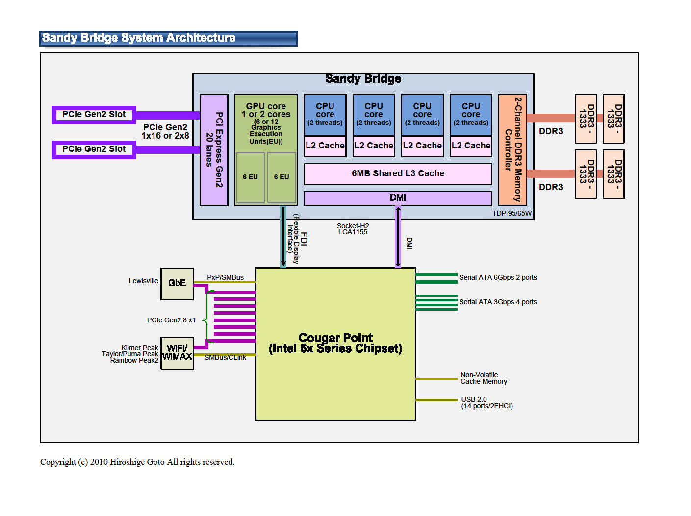
Structurally,
processor generation change
associated with the replacement of the processor socket.
The LGA 1156 connector will be replaced by the LGA connector
1155. With external resemblance and identical
sizes, these connectors are completely
incompatible with each other. Processors
will be supplied with a wide range
TDP values and frequencies in different (not
compatible with modern) cases
for new motherboards — LGA1155
(frequencies 2.3-3.4 GHz). At the same time, all produced
now motherboards will become morally
obsolete.
List of chipsets
for motherboards with LGA 1155 socket
includes models P67, H67, H61 and Q67. Remarkably,
that support for SATA 6 Gb/s will be implemented
in the southbridge, but USB 3.0 is not. Won’t be there
and the system clock generator,
also migrated to the CPU chip is
means the impossibility of overclocking through
base frequency, because it’s fixed
at 100 MHz. However, Intel leaves
the possibility of overclocking due to the multiplier,
which will be unlocked in models
with the letter K and can reach the value
57. Speaking of models — their names are the same
remain as Core i3/i5/i7, but the model number
now 4 digits. In addition to the letter K, it
can complement S (low TDP), T (even more
economical) or M (mobile). A little bit later
server and budget options will be released.
successor
processor socket LGA 1366 will become LGA
2011. Significant increase in the number
contacts is explained by the presence of
processor 256-bit memory bus
(four DDR3 channels) and integration into
northbridge function processor.
PCI-Express 2.0 interface root block
will provide system developers
boards 32 lines (the LGA-1155 will have 16 of them).
What is the result? Intel
seriously updated Nehalem — without revolutionary
breakthroughs, but simply consistently
updating microarchitecture details and
introducing all the latest innovations
two years. As a result, we got more
faster, but remaining in the same
thermal framework, processors.
Sandy
bridge,
like the old Nehalem chips
and Westmere
still have integrated
crystal pci controllers
express,
2-channel DDR3, and now also
displayport.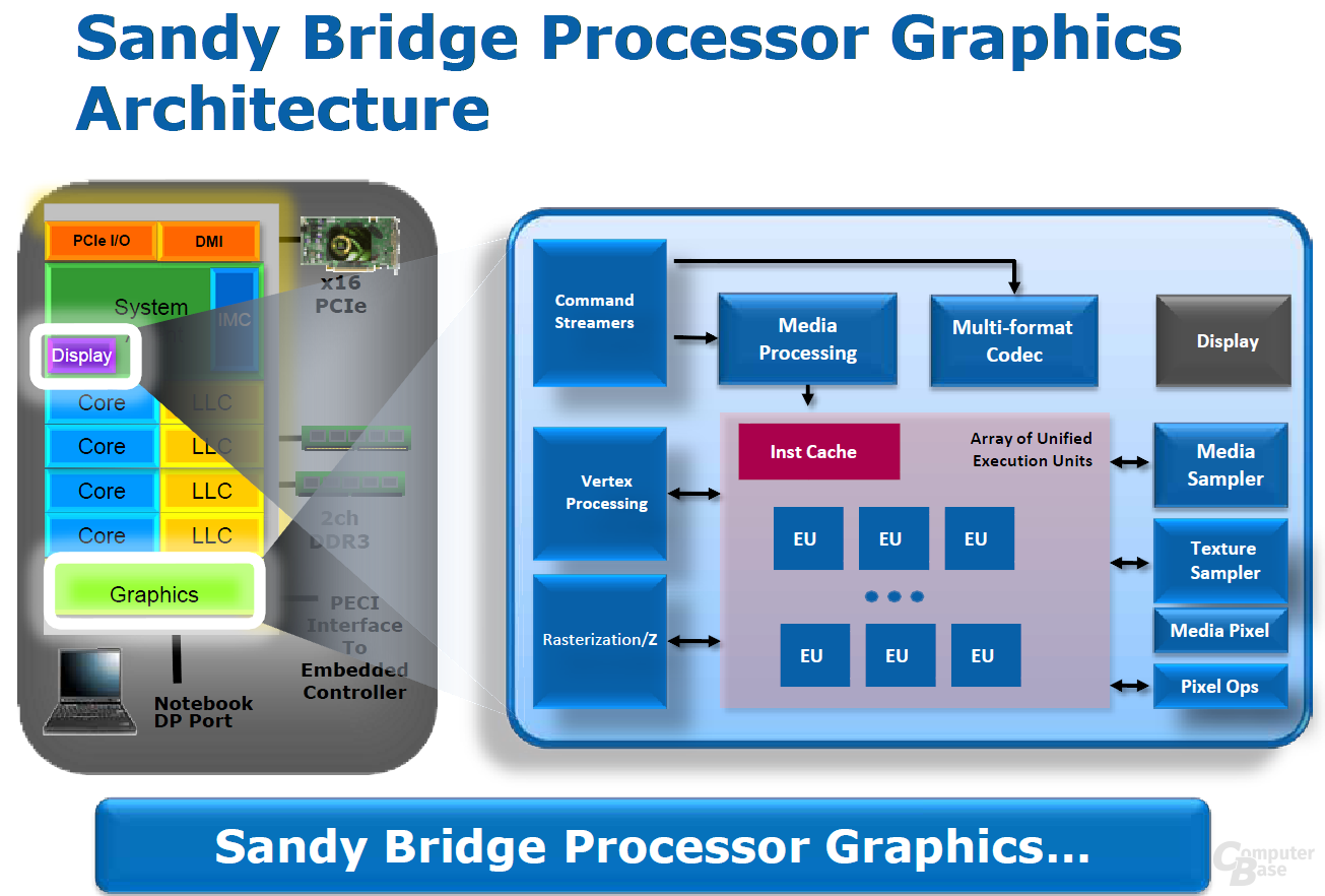
Decision to use 2-channel
memory controller taken on volume
based on the fact that the majority of clients
Intel
3 memory channels are not needed, and the LGA market
1366 is too small.
Sandy
Bridge
are the first Intel processors
with AVX instruction set support
(advanced vector extensions),
improving performance in a number of
highly parallel simple operations,
commonly used in multimedia applications.
roundabout concept
tires also greatly simplifies the creation
based on Sandy
Bridge
various crystals. For example, despite
that the prototypes of new processors
have 4 x86 processing cores, technically
very easy to make a 2-core option
or add/remove any blocks in
the future.
Server Chips
Sandy
Bridge
will be based on the same roundabout design
tires and will be able to have in the foreseeable future
many cores (chips with 10
nuclei).
Every Sandy Core
Bridge
has 256 KB of second data cache
level. To access the cache
the third level you need 25 full
machine cycles. The processor is equipped
integrated PCI Express controller
2.0 and Dual Channel Memory Controller
with support for DDR3-1600 memory. Calculated
for production according to 32 nm standards,
quad-core microprocessor will take
on a silicon crystal with an area of 225 sq. mm.
Power consumption will be 85 watts.
These
design features are believed to
will improve performance
and efficiency of Sandy processors
Bridge.
Expected that
new processors along with the transition to
new architecture will get another
nomenclature: instead of three-digit
model marking after series indication
(Core i3, Core i5, or Core i7), a four-digit
type 2XX0. So Intel
will try to avoid confusion with names
processor models of Westmere architectures
and Sandy
Bridge.
As it was said
higher, initially a new generation of processors
Intel
will be represented by five models:
-
Core i7-2600: quad-core
technology-enabled processor
Hyper-Threading, clock speed — 3.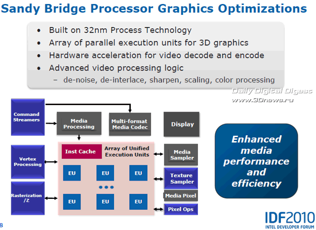 2 GHz,
third level cache — 8
MB; -
Core i5-2400: quad-core
processor without technology support
Hyper-Threading, clock speed — 3.1 GHz,
third level cache — 6
MB; -
Core i5-2500: quad-core
processor without technology support
Hyper-Threading, clock speed — 3.3 GHz,
third level cache — 6
MB; -
Core i3-2100: dual core
technology-enabled processor
Hyper-Threading, clock speed — 3.1 GHz,
third level cache — 3
MB; -
Core i3-2120: dual core
technology-enabled processor
Hyper-Threading, clock speed — 3.3 GHz,
third level cache — 3
MB.
Thus,
first models on Sandy architecture
Bridge
will be represented by dual and quad-core
technology-enabled processors
Multithreading Hyper-Threading
(or without it), operating at a frequency
over 3 GHz. Then to them, obviously,
more powerful six- and
octa-core models with 16 and 24 MB cache
third level.
System logic sets for Intel processors Oleg Nechay.
 Computerra digital magazine No. 74 [06/20/2011 — 06/26/2011]
Chipsets for Intel
processors
Oleg Nechay
Posted on June 23, 2011
The new architecture also required new logic, besides, Sandy Bridge chips are designed for installation in their own LGA1155 socket and are not compatible with sockets for the previous generation Core based on the Nehalem microarchitecture.
There are currently seven chipsets for the Sandy Bridge line on the market: Intel B65 Express, H61 Express, H67 Express, P67 Express, Q65 Express, Q67 Express and Z68 Express. The first to appear on the market were motherboards based on the H67 and P67 chipsets, a little later other modifications were released, and the flagship Z68 became the “youngest”.
Cougar Point chipsets of the first releases (revision B2) have an unpleasant story: due to a defect found in them, Intel was forced to suspend deliveries literally a month after they began.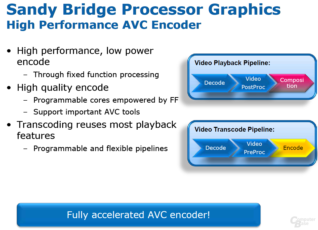 The fact is that, due to a design flaw, over time, in such chipsets, all SATA-II ports to which hard drives, solid-state and optical drives are connected could fail. At the same time, the operability of SATA-III ports was preserved, of which there are no more than two in the chipsets of the sixth series. To Intel’s credit, the company quickly recognized the problem and released upgraded chipsets (revision B3) that are free of this defect. Nevertheless, quite large batches of boards based on the defective H67 and P67 Express managed to hit the market, which affected, first of all, enthusiasts who paid a lot of money for a «hot» new product.
As in the case of the fiftieth series, the sixtieth is not a chipset, but a single chip that performs the function of the “south bridge”, that is, it serves to connect various peripherals and bears the official name PCH — Platform Controller Hub (“controller switch platforms»). The need for a «north bridge» has disappeared, since the RAM and PCI Express bus controllers, as well as the graphics core, are now built directly into the processor.
Most of the new «desktop» chipsets are capable of working with graphics integrated into the processor. They, like today’s, belong to the H series — these are the H61 and H67 sets. The only set of logic that ignores the video core built into the chip is P67, which is designed exclusively for discrete graphics: one PCI Express x16 card or two PCI Express x8 video cards.
An important difference between the new chipsets and previous generation chipsets is the doubling of PCI Express 2.0 bus bandwidth from 2.5 GT/s (gigatransfers, that is, billions of transfers per second) to 5.0 GT/s. Now the maximum speed of a single line (PCI Express x1 slot) can reach the initially provided by the standard 500 Mb/s in each direction, for a total of 1 Gb/s. This eliminates the bottleneck when connecting, for example, high-speed USB 3.0 and SATA-III controllers through PCI Express x1 slots, which is noticeable when the line speed in each direction is limited to 250 Mb / s.
Intel Z68 Express
The flagship chipset of the family, presented later than all the others — on May 11, 2011.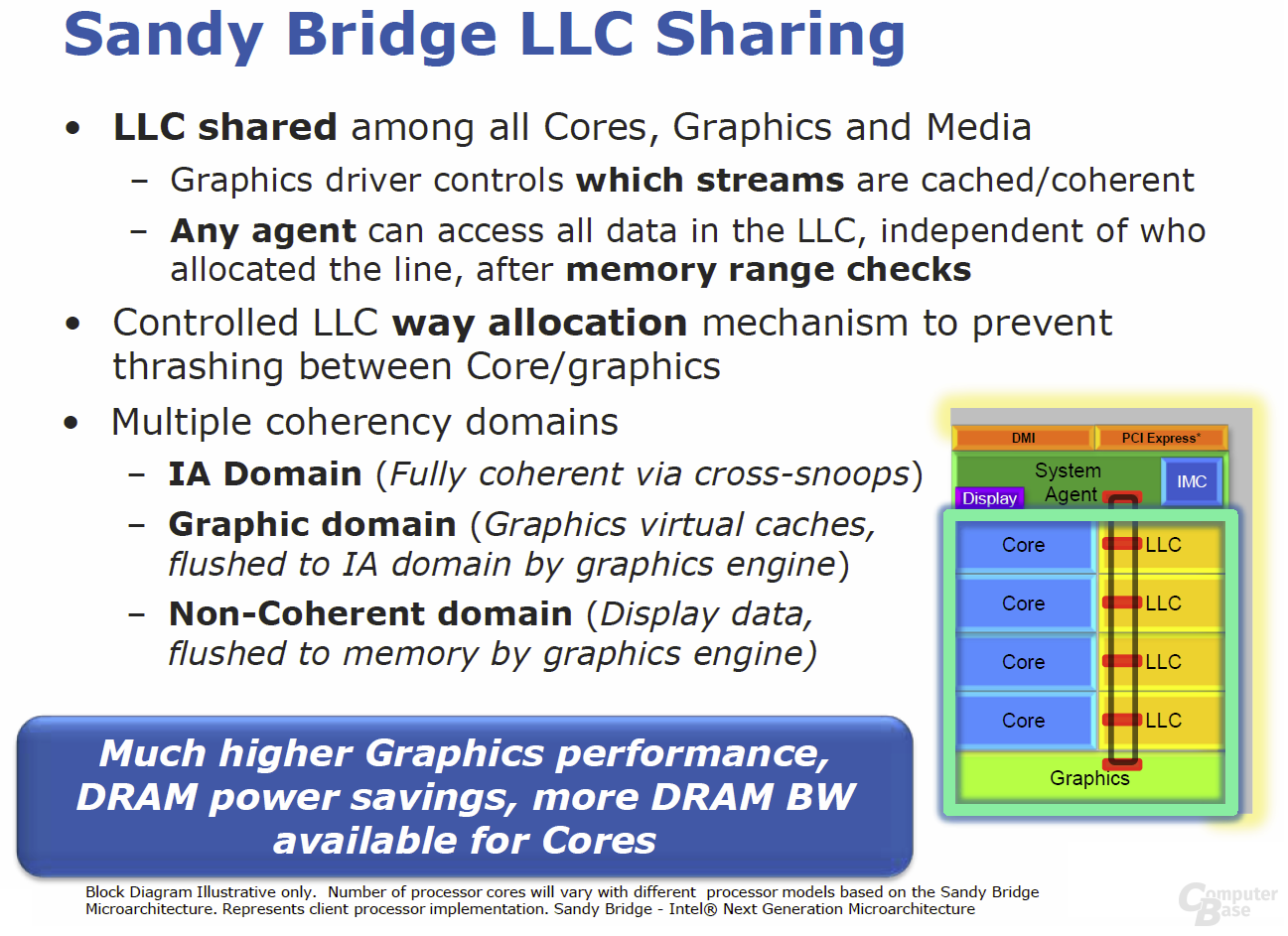 The chip combines the capabilities of all models of the line and has two features unique to the sixtieth series — Intel Smart Response Technology and Lucid Virtu. The chipset is designed for use with mid-range and high-end Core i5 and Core i7 processors for the LGA1155 socket. At the same time, according to Intel, nothing prevents installing inexpensive Core i3 chips in motherboards based on the Z68 Express, but, given the high price of such motherboards, this is unlikely to be a reasonable solution.
Intel Z68 Express Chipset Schematic
Like all Cougar Point chipsets, the Z68 is connected to the processor via a DMI 2.0 bus with a bandwidth of 20 Gb/s, or about 4 GB/s. The FDI bus is used to transmit the video signal from the integrated processor graphics. Many video interfaces are supported, including HDMI, DVI and DisplayPort. Supports eight full-speed PCI Express 2.0 x1 ports. It is possible to install both one (PCI Express x16) and two graphics accelerators (PCI Express x8 + x8) in SLI and CrossFire modes.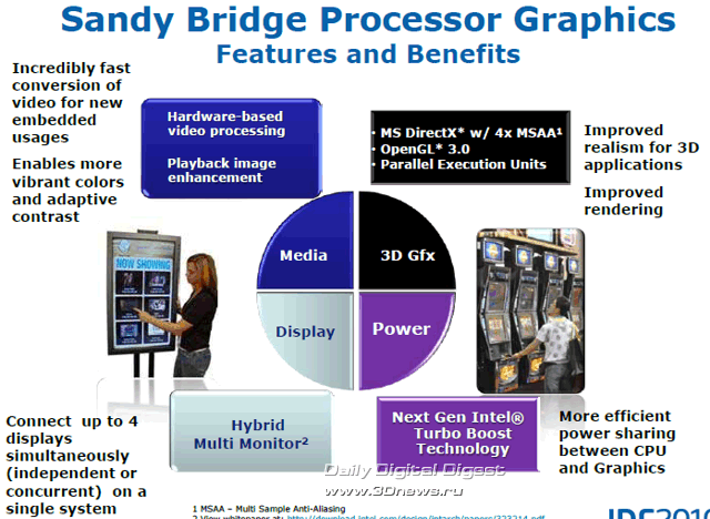
The chip implements a Serial ATA controller for 2 SATA III (6 Gb/s) ports and four SATA II (3 Gb/s) ports, supports RAID levels 0, 1, 0+1 (10), and 5 and technology Matrix RAID (hybrid mode, when different parts of the same set of disks are used as arrays of different levels). There is a multi-channel (7.1) High Definition Audio sound controller, a USB 2.0 controller for fourteen ports, a gigabit network MAC controller, as well as interfaces for connecting various low-speed peripherals.
Characteristically, the Z68 Express, like almost all chips of the family, lacks a PCI controller; it also lacks the expected USB 3.0. The rejection of obsolete PCI is quite understandable, but Intel’s stubborn reluctance to integrate USB 3.0 into the chipset can only be explained by its intention to promote an alternative Thunderbolt interface. However, motherboard manufacturers install PCI and USB 3.0 controllers on their products, so this will not create a problem.
The Intel Z68 Express chipset provides the widest overclocking options in the line: if desired, you can increase the value of the core and RAM multiplier, increase the voltage and allowable temperature, as well as the frequency of the integrated graphics core.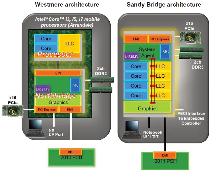
Only this sixtieth series logic model features Intel Smart Response Technology and Lucid Virtu. The first of them allows you to use a small SSD (from 20 GB) for caching various data, thereby increasing the speed of the system, and the second makes it possible to switch between integrated and discrete graphics — a system similar to the NVIDIA Optimus laptop.
According to the first reviews, the use of Intel Smart Response on average allows you to speed up the work with applications in Windows 7 and Vista (it is only compatible with these operating systems) by about half, but, of course, it does not give such a significant increase as when installing the entire system on an SSD. The usefulness of Lucid Virtu raises serious doubts: if switching to integrated graphics in a laptop can save battery power, then it is meaningless for a stationary desktop. I can personally see the point in periodically switching to integrated graphics only if you have a couple of powerful video cards and you don’t want to hear the hum of their cooling system when surfing the Internet or when working with documents.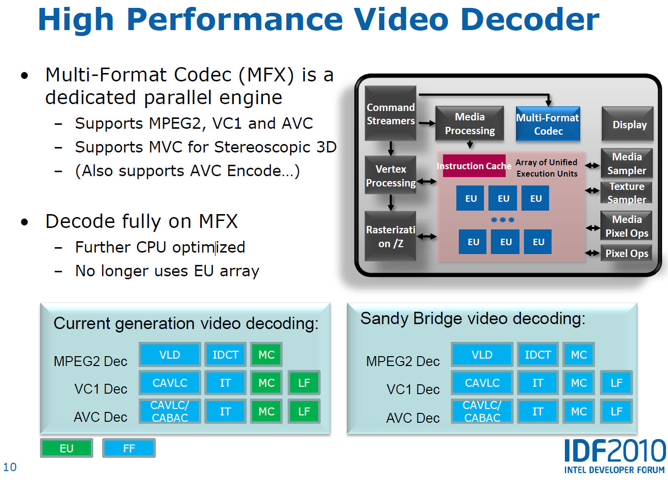 As for the support of Intel Quick Sync video transcoding technology even when working with discrete video, it is generally rather strange to present it as an advantage.
The stated thermal package for the Intel Z68 Express chip is 6.1 W, as, indeed, for all other representatives of the sixtieth series.
Intel P67 Express
This chipset was introduced simultaneously with the presentation of the Sandy Bridge platform on January 9, 2011 and, along with H67, became one of the two most controversial in the family. The fact is that this is the only chipset of the sixtieth series that does not support the graphics core built into the processor — it simply does not have an FDI bus. Considering that the graphics are integrated into all Sandy Bridge CPUs without exception, this looks more than strange.
Intel P67 Express Chipset Schematic
Otherwise, this is a powerful «south bridge», which is not much inferior in capabilities to the flagship Z68 Express, which appeared much later. Prior to the release of Z68, this chipset was the only one in the family that allowed installing two discrete PCI Express 2.0 x8 + x8 video cards, as well as freely overclocking the processor and RAM. Supports eight full-speed PCI Express 2.0 x1 ports.
The
P67 Express connects to the processor via a DMI 2.0 bus with a bandwidth of 20 Gbps. The chip has a Serial ATA controller with 2 SATA III ports (6 Gb / s) and four SATA II ports (3 Gb / s), support for RAID levels 0, 1, 0 + 1 (10) and 5 and Matrix RAID technology . A multi-channel (7.1) High Definition Audio controller, a fourteen-port USB 2.0 controller, a gigabit network MAC controller, as well as interfaces for connecting various low-speed peripherals are provided.
Intel H67 Express
The H67 Express system logic set, released on January 9, 2011, practically does not differ from the P67 Express, except for the ability to work with video integrated into processors (that is, the presence of the FDI bus) and the lack of support for two discrete video cards.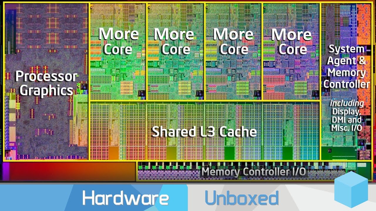 Despite the fact that the PCI Express 2.0 controller itself is built into the processors, Intel considered it necessary to introduce such a restriction for some reason. One way or another, H67 Express provides for the installation of only one discrete graphics accelerator PCI Express 2.0 x16. Eight full-speed PCI Express 2.0 x1 ports are also provided.
Intel H67 Express chipset diagram
Another little-explained feature of this chipset is the impossibility of overclocking the processor and RAM. But here you can increase the frequency of the graphics core built into the processors. Simply put, this chipset is definitely aimed at those who intend to use only embedded video.
As you can see, the functionality of the P67 Express and the H67 Express was combined in the flagship Z68 Express, released five months later. Those who rushed to buy a motherboard based on one of the early chipsets have to put up with strange compromises imposed by Intel marketers for some unknown reason.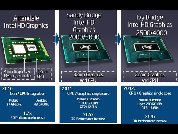
In all other respects, the H67 Express repeats the P67 Express: a DMI 2.0 system bus with a bandwidth of 20 Gb / s, a Serial ATA controller for a pair of SATA III ports (6 Gb / s) and four SATA II ports (3 Gb / s), support for RAID levels 0, 1, 0+1 (10) and 5 and Matrix RAID technology, multi-channel (7.1) High Definition Audio sound controller, fourteen-port USB 2.0 controller, Gigabit network MAC controller, as well as interfaces for connection low speed peripherals.
Intel H61, Q67, Q65 and B65 Express
Intel H61, Q67, Q65 and B65 Express are four chipsets that are simplified compared to those described above and are aimed at use in office and other computers that are part of corporate networks. Three of them, namely Q67, Q65 and B65 Express, are equipped with an integrated PCI 2.3 controller with support for up to four ports.
Intel H61 Express chipset diagram
The simplest modification, H61 Express, boasts support for integrated graphics (FDI bus) and one discrete PCI Express 2.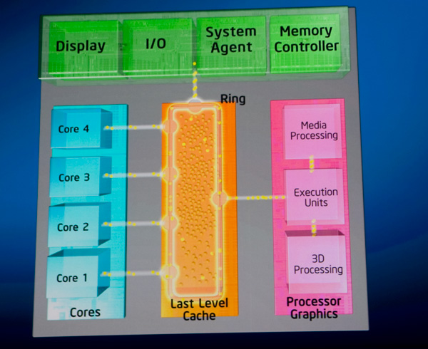 0 x16 card, six PCI Express 2.0 x1 ports, a DMI 2.0 system bus with a bandwidth of 20 Gbps / s, a Serial ATA controller for four SATA II ports (3 Gb / s), a multi-channel (7.1) High Definition Audio controller, a ten-port USB 2.0 controller, a gigabit network MAC controller and interfaces for connecting low-speed peripherals.
Intel H65 Express chipset diagram
B65 Express chipset features eight PCI Express 2.0 x1 ports, Serial ATA controller for two SATA III ports (6 Gb/s) and four SATA II ports (3 Gb/s), RAID support — arrays of levels 0, 1, 0 + 1 (10) and 5 and Matrix RAID technology, a twelve-port USB 2.0 controller and the ability to subscribe to remote services for servicing corporate PCs Intel Level III Manageability Upgrade.
Intel Q65 Express Chipset Schematic
Intel Q67 Express Chipset Diagram
The Q65 Express chipset differs from the B65 Express by already fourteen USB 2.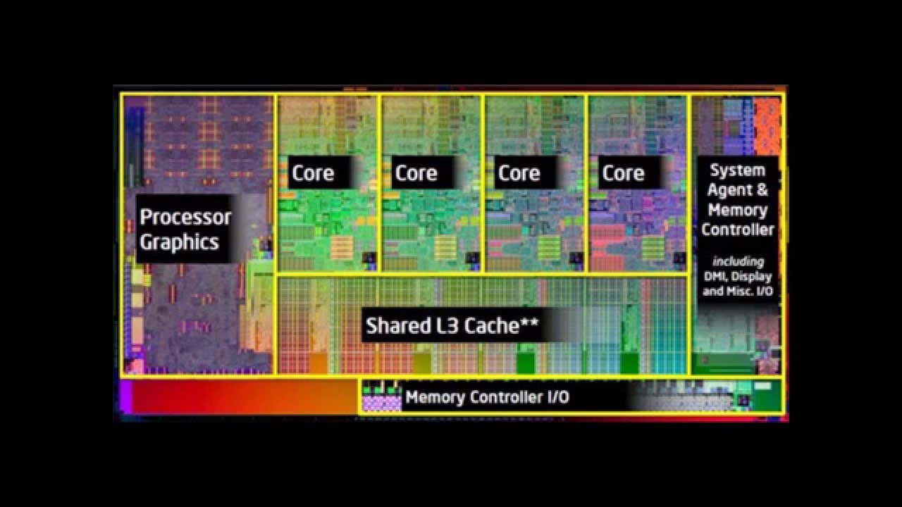 0 ports and the ability to order the Intel Standard Manageability corporate services package. The Q67 Express is further supported by Intel Trusted Execution Technology and Intel Rapid Storage, as well as Intel Active Management Service.
In the next article we will talk about several interesting motherboards based on Intel sixtieth series chipsets.
To the table of contents
Chipsets for AMD desktop processors Oleg Nechay
Chipsets for AMD desktop processors
Oleg Nechay
Posted on June 27, 2011
Presentation of chipsets 990FX, 990X and 970 took place on June 1, 2011, and the first motherboards based on them were demonstrated at the same time, in early June,
A Guide to New Intel Processors (Part 2) Oleg Nechay
A Guide to New Intel Processors (Part 2)
Oleg Nechay
First, we will highlight the most important features of each Intel Core i3/i5/i7 processor family, and then we will talk about which of these chips are of particular interest.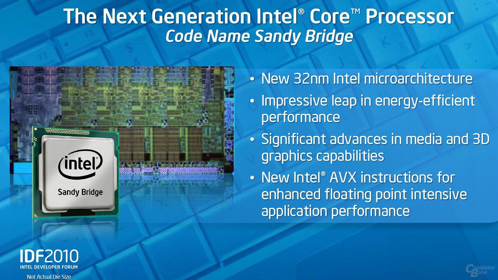 For the convenience of readers, we counted
CES 2012: news from AMD, Intel and Nvidia Oleg Nechay
СES 2012: news from AMD, Intel and Nvidia
Oleg Nechay
Posted on January 20, 2012
Intel
Intel Corporation presented at CES 2012 its new mobile platform for smartphones Medfield and shared information about plans to actively market the new
Intel: from a chip manufacturer to a solution provider Oleg Nechai
Intel: From Chip Manufacturer to Solution Provider
Oleg Nechay
Posted May 17, 2010
On May 11, Intel held another annual conference for investors, at which the new status of the corporation was proclaimed: due to the expansion of areas of activity,
Motherboards for the Intel platform Oleg Nechay
Motherboards for the Intel platform
Oleg Nechay
Posted on June 24, 2010
In the first part of this review, we described the main characteristics of Intel’s «fiftieth series» desktop chipsets, and now let’s talk about specific models of motherboards based on
Motherboards for the Intel Sandy Bridge platform Oleg Nechay
Motherboards for the Intel Sandy Bridge platform
Oleg Nechay
Posted on June 24, 2011
In the first part of this review, we got acquainted with the main characteristics of the sixtieth series of Intel chipsets, code-named Cougar Point, and
Intel hopes to double Moore’s law Oleg Nechay
Intel hopes to double Moore’s law
Oleg Nechay
Posted on May 19, 2011
At the regular meeting with investors and analysts held on May 17, 2011, Intel CEO Paul Otellini announced a revision of plans for the release of
CES 2011: What Intel, AMD and NVIDIA brought to the exhibition Oleg Nechay
CES 2011: What Intel, AMD and NVIDIA brought to the show
Oleg Nechay
Posted on January 11, 2011
AMD
Just before the start of CES 2011, AMD introduced several completely new chips: APU Fusion processors, updated quad and
Probabilistic processor: the triumph of Bayesian logic Oleg Nechai
Probabilistic Processor: The Triumph of Bayesian Logic
Oleg Nechay
Posted August 23, 2010
The engineers of the American company Lyric Semiconductor announced the creation of a technology that can revolutionize the usual logical design
Chipsets for AMD processors Oleg Nechay
Chipsets for AMD processors
Oleg Nechay
Posted on June 28, 2010
The most common AMD 7xx series chipsets for the K10 architecture appeared on the market quite a long time ago: the first chipsets were introduced back in the fall of 2007 —
Sandy Bridge: Next Generation Intel Microarchitecture Oleg Nechay
Sandy Bridge: Next Generation Intel Microarchitecture
Oleg Nechay
Posted byOleg Nechay
In the first quarter of 2011, Intel plans to introduce a new CPU microarchitecture, codenamed Sandy Bridge. This is
Chipsets for new Intel desktop processors Oleg Nechay
Chipsets for new Intel desktop processors
Oleg Nechay
Posted on June 18, 2010
The new line of «desktop» central processors Intel Core i3/i5/i7 required the creation of new sets of system logic. Historically, the top
appeared first
Mobile World Congress: Nvidia, Intel and ST-Ericsson Oleg Nechay
Mobile World Congress: Nvidia, Intel and ST-Ericsson
Oleg Nechay
Posted on February 18, 2011
The most notable innovations include Nvidia Kal-El and Intel Medfield «systems-on-a-chip», ST-Ericsson processors, platforms and modems for mobile devices, as well as Intel XMM 7060, XMM
mobile platforms
Hardware trojans for Intel processors — the first practical implementation Andrey Vasilkov
Hardware trojans for Intel processors — the first practical implementation
Andrey Vasilkov
Published on September 19, 2013
Eight years ago, the U.