ABIT PD5N SiS 5598 Socket-7 Board
by Anand Lal Shimpion December 10, 1997 7:20 PM EST
- Posted in
- Motherboards
0 Comments
|
0 Comments
IndexFeatures
MTech held the high ground for
some time with their Mustang being the only truly successful motherboard based on a
proprietary design concocted by Silicon Integrated Systems, otherwise known as SiS.
MTech based their entire Mustang design around the single chip solution of the SiS Trinity
5571 chipset. However MTech now has some competition for the throne, with ABIT’s
introduction of their next generation SiS 5598 based all-in-one PD5N
motherboard. How well does it compare to the competition? Does MTech finally
have a worthy competitor for the SiS throne? Let’s find out. ..
Motherboard
Specifications
| Socket
Style: |
Socket 7 |
| Chipset: | SiS 5598 |
| Cache: | 512KB |
| Form
Factor: |
AT (w/ AT &
ATX PS Connectors) |
| BUS
Speeds: |
50 / 55 / 60 / 66
/ 68 / 75 / 83 MHz |
| Clock
Multipliers: |
1. 5x / 2.0x / 5x / 2.0x /
2.5x / 3.0x / 3.5x |
| Voltages
Supported: |
2.8 / 2.9 / 3.2 /
3.38 / 3.5 |
| RAM
Slots: |
4 72pin SIMM
Slots (EDO/FPM) |
| PCI/ISA
Slots: |
4 PCI Slots 3 ISA Slots |
| BIOS: | AWARD PnP BIOS |
| PCI
EIDE Controller: |
Super I/O 2 EIDE Channels 1 FDD Channel 2 Serial /1 EPP |
The Good
When ABIT referred to their new PD5N as an all
in one motherboard they weren’t kidding at all. The PD5N integrates the standard, 4
PCI and 3 ISA slots, with the onboard SiS 5598 Busmastering PCI IDE Controller, as well a
speedy SiS True Color PCI VGA Graphics accelerator! This almost completely
eliminates the need for a third party video adapter, however as you will be able to tell
by the Winstone scores in the Test the onboard VGA controller is no match for a genuine
Matrox. Fully configurable via the AWARD PnP BIOS Setup Utility, the VGA controller
is connected to the motherboard via a low profile cable included with the PD5N.
The PD5N seems to break a lot of traditional
ABIT practices found and implemented in their most popular motherboards like the AX5 and
the IT5H. Like ABIT’s newest TX motherboard the TX5N, the PD5N provides users with a
easy to use alternative to the popular SoftMenu Jumperless CPU Configuration ABIT has
graciously spoiled us all with. Instead of being tediously configured via jumpers,
the PD5N can be completely setup using 2 sets of Dip Switches (8 switches in each set)
with one set used to configure the Voltage settings and the other used to set the bus
speed and clock multiplier. The PD5N I received did not have a user’s manual,
however that was because it was one of the first out on the market it wasn’t shipped with
one, any PD5N units you’ll purchase will have the classic ABIT manual which will provide
you with hours of fun filled reading 😉
After setting up the hardware side of the
PD5N, configuring the BIOS isn’t that much of a task although it is a little different
that what most people are used to with the AWARD BIOS. Upon bootup, if using the
onboard VGA controller (which can easily be disabled by plugging in your own video card
and unplugging VGA connector cable) the BIOS not only displays the amount of system memory
but also the amount of RAM shared by the video adapter (by default it is set to 1MB
although it can be changed via the BIOS setup). Using the AWARD Setup utility, you
can also modify the memory clock of the onboard VGA accelerator, however when taken up to
70MHz (the maximum setting) some instability might result so be careful. On a side
note, the onboard VGA Accelerator isn’t fully supported by Linux, however since it is
based on the VESA specification you can simply select the VESA VGA driver or Standard VGA
under X.
The features of any motherboard are made
possible, for the most part, by the chipset it is designed around. The PD5N, as
mentioned earlier, is designed around the new SiS 5598 chipset which is a variant of the
SiS 5597 chipset. Unfortunately, very little is known about the SiS 5598 chipset
other than the obvious. Take a look at the chipset guide for a complete list of
features the 5597/5598 supports. Here is an abridged list of features specific
to the PD5N:
-
onboard VGA controller
-
onboard USB controller
-
Support for the 75MHz bus speed and
Asynchronous PCI Bus -
Support for UltraDMA Hard Drives
The performance and stability of the PD5N is
about average for a motherboard based on a non-Intel chipset (excluding VIA based
motherboards which simply rock), its undocumented support for the 83. 3MHz bus speed (the
83.3MHz setting is: SW6 — ON SW7 — ON SW8 — ON, on the bus speed dip switch) makes it an
even better value for those looking for an all-in-one solution for a low cost
system.
The Bad
Although the SiS 5598 chipset fully supports
SDRAM, actual SDRAM slots are mysteriously missing from the PD5N. This could
indicate problems with the SiS 5598 and SDRAM, or just an attempt to reduce the cost of
the motherboard. Another disappointment is the lack of support for the Cyrix/IBM
Linear Burst Mode as found in other SiS Chipsets. SiS doesn’t even mention future
support for linear burst mode on their homepage, which is sad for the most part because
that was one of the 5571’s trademark features. Of course that isn’t a fault of the
motherboard, rather the chipset, however for all of you 6×86 and 6x86MX users out there,
don’t expect to see bone shattering performance with the PD5N, although it is fairly
competitive with those two processors.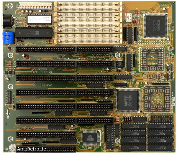
Features
IndexFeatures
Tweet
PRINT THIS ARTICLE
Full Yes SIS 5598 TX/VGA
Full Yes SIS 5598 TX/VGA
DescriptionDownloadsCPUs
Form factor
Baby-AT (max 220 x 330mm)
PSU connector
AT-Style (P8-P9), ATX 1.x (20-pin ATX)
Chipset
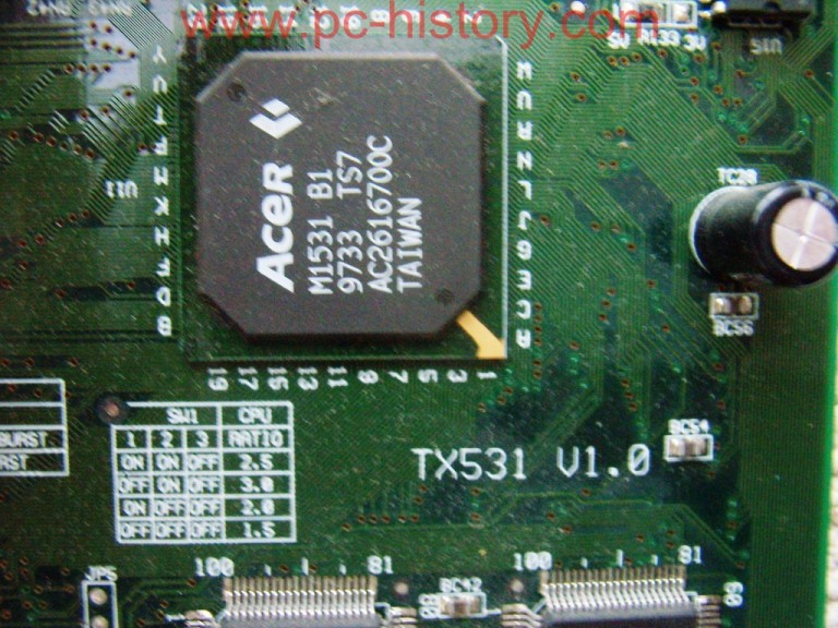
SiS 5597/5598 ((Jedi) Pentium PCI/ISA Chipset)
Chipset parts
SiS 5597
SiS 5598
Dimensions
Unknown
CPU socket
Socket 7 (PGA321)
CPU platforms
Pentium (P54)Pentium MMX (P55)
Supported FSB speed
50MHz
Cache
256 KB
, 512 KB
Supported RAM size
384 MB
Supported RAM types
SDR UDIMM, 168-pin EDO UDIMM
Video chipset
SiS 5598 (SiS 6326)
(4MB max VRAM)
I/O ports
1x
Floppy interface
2x
IDE interface
1x
PS/2 keyboard
1x
Parallel
2x
Serial
2x
USB 1. x
x
1x
VGA
1x
AT Keyboard
Expansion slots
4x
32-bit PCI
3x
16-bit ISA
Last updated 2022-06-19T07:30:05Z
Drivers:
3 entries
Language
Media type
OS Compatibility
Name
Version
1x
Windows 95
Windows 98
Windows ME
Windows NT 3.5
Windows NT 4.0
Windows 2000
SiS 5598 IGP Driver
1.13
1x
Windows 95
Windows 98
Windows ME
Windows 2000
Windows XP
SiS IDE Driver (New Chipsets)
2. 04A
04A
1x
MS-DOS 6.22
OS/2 Warp 3.0 ?
OS/2 Warp 4.0
Windows NT 3.1
Windows NT 3.5
Windows NT 4.0
Windows 95
Windows 98
SiS IDE Driver (Old Chipsets)
2.13
BIOS images:
1 file
Manuf.
POST String
Note
Core Ver.
BIOS Ver.
Award
10/30/97-SiS-5598-SMC37C-2A5IIF3AC-00
1.04A
4.51PG
4.1
Documentation:
2 entries
-
SIS 5598 TX Jumper Settings
(English) -
SIS 5598 TX Jumper Settings
(English)
Model
Speed
FSB
Voltages
L1 Cache
L2 Cache
L3 Cache
Core
Process
TDP
AMD K5 PR75
75MHz
50MHz
3. 5V
5V
24KB
—
—
SSA/5
350nm
—
Intel Pentium 75
75MHz
50MHz
3.3V
16KB
—
—
P54C
600nm
—
No NPUs listed.
Image 1 of 1
Disclaimer
The info found in this page might not be entirely correct. Feel free to amend this page by logging in, contacting us on Discord or via email.
New SiS chipsets
Silicon Integrated Systems Corporation, the former leading manufacturer of chipsets for boards based on the 486 processor, quickly lost its rights with the release of the Pentium processor. But this does not mean that now no one takes into account its products. Quickly refocusing on the production of cheap chipsets, SiS occupied its niche in the market. The company has now announced the SiS5581, SiS5591, SiS5597 chipsets for Pentium systems and SiS5602 for Pentium II systems.
SiS5581
Designed for systems based on Pentium processors, this chipset is made as a single BGA chip (5581 or 5582, differing in pin arrangement) and contains keyboard, USB and RTC controllers.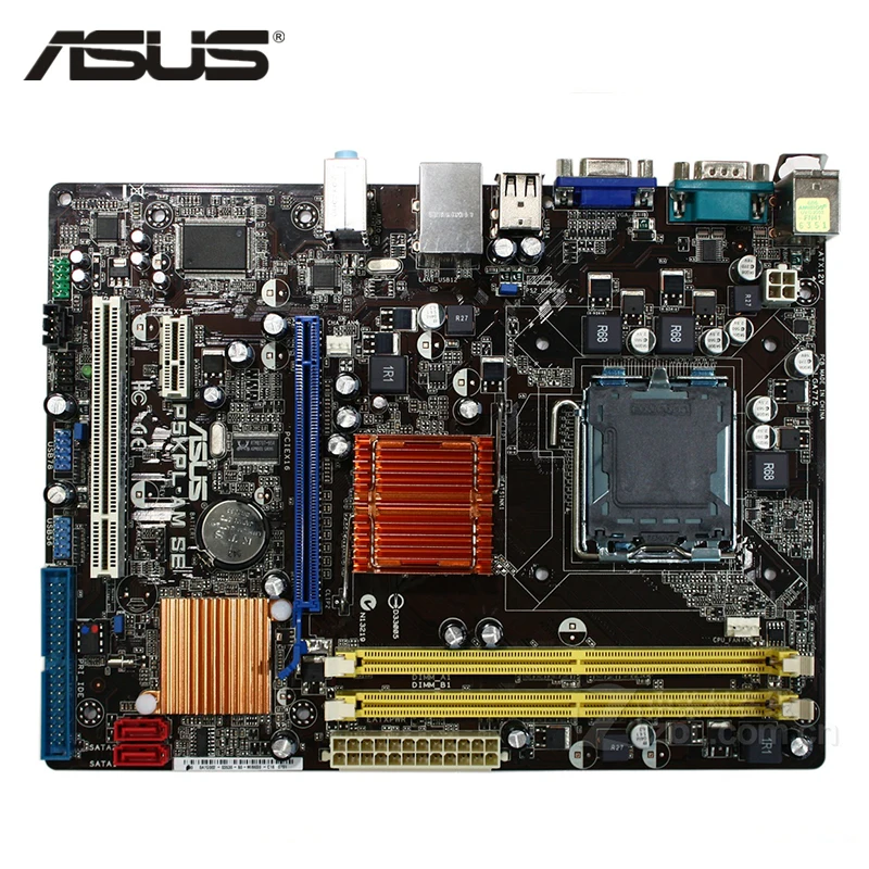 With low cost, it supports external bus frequency up to 75 MHz and ACPI (Advanced Configuration and Power Interface) power saving standard. Also supported are the Ultra DMA-33 specifications for the embedded IDE controller and Common Architecture, which is designed to port ISA functions to PCI, which is required by the PC9 specification.8.
SiS5581 Highlights
- Supports bus speeds up to 75MHz
- Integrated DRAM Controller supporting FPM/EDO/SDRAM DRAM
- Integrated L2 Cache Controller
- Integrated Host-to-PCI and PCI Bridges ISA
- Integrated PCI dual-channel IDE controller
- Integrated Legacy PMU and ACPI controllers
- Integrated write-back and prefetch buffers for increased performance
- Integrated USB controller
- I2C bus support for SDRAM and frequency synthesizer
- Integrated ISA controller
- Integrated keyboard controller
- Integrated real time clock (RTC)
- High-tech chip implemented as 480-pin BGA
- 0.
 35 µm technology
 - Supply voltage 3.3V
SiS5591
The second of the chipsets that appeared after the VIA VP3, designed for Pentium systems, supporting the AGP port. It should be noted that, in particular, due to the internal architecture, this chipset is recommended for use in conjunction with a Cyrix processor.
- Supports 6 RAS lanes for FPM/EDO/SDRAM DIMMs/SIMMs
- Supports 2MB to 768MB main memory
- Supports 256k/512K/1M/2M/4M/8M/16M/32M memory modules
- Support for 3.3V and 5V modules
- Timing chart for FPM DRAM when reading 5/6-3-3-3(-3-3-3-3)
- Timing chart for EDO DRAM when reading 5/6-2 -2-2(-2-2-2-2)
- Timing diagram for SDRAM when reading 5/6/7/8-1-1-1(-2-1-1-1)
- When writing X-1-1-1/X-2-2-2/X-3-3-3 timing
- Support up to 5 PCI Bus Master devices
- Support direct access between CPU/L2 and AGP/Memory
- Direct access support between CPU and Memory, and between two PCI devices
- Synchronous and asynchronous PCI support
- IDE 9 write-back support0014
- Support for pipelined access between CPU and PCI
- Support for advanced PCI Bus Mastering
- Support for pipelined access between CPU and AGP
- Support for advanced access to AGP 9013 memory channels 9013 to 16-piece GRLT(Graphics Remapping Lookaside Table) to increase AGP performance
- Support for PCI-to-PCI memory bridge functions used when accessing AGP
- CPU-to-Memory Write Buffer (CTMFF) size — 8 QWord
- CPU-to-Memory Read Buffer size — 4 QWord
- CPU-to-PCI Write Buffer size (CTPFF) — 8 QWord
- PCI-to-Memory Write Buffer (CTPFF) Size — 8 QWord
- PCI-to-Memory Read Buffer (CTPFF) Size — 8 QWord
- Embedded KBC/RTC/USB
 35µm technology and 9013V 0.35V chip 5595 : 208-pin 0.5µm PQFP 5V
 Competitive Comparison
| SiS5591 | Intel 430TX | VIA VP3 | ||||||
|---|---|---|---|---|---|---|---|---|
| Package | 1 x PQFP, 1 x BGA | 1 x PQFP, 1 x MBGA | 1 x PQFP, 1 x BGA | |||||
| Dual/Multi CPU Support | no | no | no | |||||
| Max. L2 Cache Size | 1024 kB — Pipelined Burst | 512 kB — Pipelined Burst | 2048 kB — Pipelined Burst | FPM, EDO, SDRAM | FPM, EDO, SDRAM | |||
| Max. DRAM | 768 MB — 6 RAS lines | 256 MB — 6 RAS lines | 1024 MB — 8 RAS lines | |||||
| Max. Cacheable DRAM | 768 MB | 64 MB | 1024 MB | |||||
| 5-3-3-3 | 5-3-3-3 | |||||||
| EDO RAM | 5-2-2-2 | 5-2-2-2 | 5-2-2-2-2-2 | |||||
| Bedo RAM | N/A | N/A | N/A | |||||
| SDRAM | 5-1-1-1-1-1-1-1-1-1-1-1-1-1-1-1-1-1-1-1-1-1-1-1-1-1-1-1-1-1EV 1-1 | 5-1-1 | ||||||
| DRAM ECC Support | NO | No. |
YES | |||||
| DRAM REPHIE0173 CAS before RAS | CAS before RAS | CAS before RAS | ||||||
| No. of CPU Write Buffers | 8 QW = 64 Byte | 5 QW = 40 Byte | 32 QW = 256 Byte | |||||
| PCI Specification | 2.1 | 2.1 | 2.1 | |||||
| Asynchronous PCI Timing | yes | n/a | n/a | |||||
| Max. no. of PCI Masters | 5 | 5 | 5 | |||||
| No. of CPU to PCI Buffers | 8 DW = 32 Byte | 5 DW = 20 Byte | 6 DW = 24 Byte | |||||
| of PCI to DRAM Buffers post/prefetch | 8 DW = 32 Byte / 8 DW = 32 Byte | 10 DW = 40 Byte / 18 DW = 72 Byte | 48 DW = 192 Byte / 48 DW = 192 Byte | |||||
| USB Support | yes | yes | yes | |||||
| ATA-33 Extension | yes | yes | yes | |||||
| PIO Master/Slave Independent Drive Timing | yes | yes | yes | |||||
| DMA Bus Master Support | yes | yes | yes | |||||
AGP Support0440
SiS5597 While dominating the Socket 7 chipset market, SiS was able to maintain a market share with the release of chipsets with integrated video. In addition to video, this chipset also integrates a keyboard controller, a real-time clock and a USB controller. In addition, as in most chipsets from this company, the frequency of 75 MHz and the advanced power management standard Advanced Configuration and Power Interface (ACPI) are officially supported. The integrated IDE controller supports the Ultra DMA-33 specification and the integrated I/O controller complies with the Common Architecture. The chipset is available as a single BGA chip, 5597 or 5598, depending on configuration. SiS5581 Highlights
SiS5602The SiS 5602 chipset is designed for systems based on the Pentium II processor. It is made in the form of a single 560-pin chip, made according to 0.35 micron technology, and contains a 64-bit video accelerator, a real-time clock controller with 256-byte CMOS, a keyboard controller, a dual-channel IDE controller, and a USB controller. This chipset fully complies with and supports PC9 specifications.7, Ultra DMA/33 and GTL+ Host Bus. Supported from 2 MB to 512 MB of all types of memory — FP/EDO/SDRAM in DIMM and SIMM modules. Spec:
May 22, 1998 News
News section > TX Pro, VX Pro and more — what are you?Iron Author: AK While working on bringing my retro Pentium II PC back to life, I ran into an interesting problem. There was a strange name BX Pro on the chipset heatsink and at first I thought that we were talking about some kind of Intel BX chipset. Fortunately, at the time of the Pentium II-III it was an excellent and stable chipset. But in the end, the casket opened in a completely different way. A video about this computer can be seen below.
| ||||||||
 SiS5597 continues this line and implements shared memory technology for the video card. This means that not only a motherboard is purchased for a small price, but also a video card that does not need additional video memory due to the use of system memory.
  35 micron technology
  1 compliant with 5V 33MHz interface
  The first comparative tests have appeared