Kaby Lake overclocking tested: the quest for 5GHz
Kaby Lake. (That’s ‘Kaby rhymes with baby’ if you’re wondering, according to my press contact over at Intel, though I’ve heard it called ‘Cabbie’ Lake by more than a few folks.) Intel’s 7th Generation Core processors are now available for everything from 2-in-1 devices to laptops to full blown desktops. And what do you get with the new generation of parts? My Kaby Lake overview covers that, but the main story for desktop users is that Kaby Lake increases the clock speeds and clock speed range of Skylake. This is thanks to refinements in Intel’s 14nm manufacturing process, and if you’re wondering how much junk is left in the trunk, that’s what I’m here to explore.
Intel has had unlocked ‘enthusiast’ processors for a while now, but users interested in a budget-friendly option have generally been left out. The Pentium G3258 Anniversary Edition is the one exception, a chip that could overclock well but which was hobbled by a pure dual-core configuration and limited L3 cache. Intel is trying something new with Kaby Lake, bringing out a Core i3 K-series part that supports overclocking. The only problem: it’s priced too high to really qualify as a budget option. The Core i3-7350K costs $168 (for 1000 units, so it’ll be a bit more at retail initially), compared to the i5-7600K ($242) and i7-7700K ($339). There are other potential options as well, which I’ll return to in a minute.
Before we get any deeper, anyone new to overclocking needs to understand a few things. First, overclocking results are never ‘guaranteed,’ so even if everyone and their dog is able to run at 5.0GHz, you might get a dud chip that tops out at 4.8GHz. Trust me on this: it happens, and it’s not the end of the world. That goes double now that we’re looking at overclocks that amount to around two percent more performance for every 100MHz. Second, if you screw up your chip via overclocking (which is pretty unlikely these days, unless you shove too much voltage down its throat), it’s on you—the default warranty doesn’t cover overclocking (though you can purchase a protection plan if you want to). Or you can buy a boutique PC that comes factory overclocked.
The third point is where things start to get a bit nebulous. Overclocking depends on many factors, including your particular chip, but also your motherboard, CPU cooling, and even less obvious factors like memory and power supply. Basically, don’t skimp on most areas and you should be fine. I’m not doing anything exotic here, so if you want to see results with liquid nitrogen (LN2), sorry. Instead, I’m looking at the sort of overclocks most people will go after with a good closed-loop cooler. Let’s talk about the test platforms a bit.
Meet the hardware
I have Corsair’s 280mm Hydro 115i closed-loop liquid cooler for the CPU, which should provide ample cooling for most users. For overclocking, I erred on the side of aggressive cooling and set Corsair’s Link software to ‘Performance’ mode rather than ‘Balanced’ or ‘Quiet.’ However, I do have to note that the current version of Link doesn’t detect Kaby Lake processors—it doesn’t show or monitor CPU temperatures, so I had to set fan speed manually.
MSI’s Z270 Gaming M7
Overclocking Hardware
MSI Z270 Gaming M7
Core i7-7700K
Core i5-7600K
Core i3-7350K
Corsair Hydro h215i
Corsair Dominator Platinum 2x8GB DDR4
GeForce GTX 1080 FE
Samsung 960 Pro 512GB
Samsung 850 Pro 2TB
Corsair Carbide Air 740
Corsair RM650X
Asus Z170-A
ASRock Z170 Gaming K6
Core i7-6700K
Corei i5-6600K
Core i5-6400
On the motherboard front, I’m using MSI’s Z270 Gaming M7 for the KBL parts. This is a board that sits near the top of MSI’s ‘mainstream’ Z270 line, with their ‘Godlike’ line of motherboards designed for those who want to take things to the next level (LN2), but pricing makes those an extremely niche product. The M7 features RGB lighting, auto-overclocking support that can try for up to 5.2GHz if you crank the dial to 11 (no, it didn’t work for me), and a nice collection of other features like triple M.2 slots.
I’ve done limited testing with a few other motherboards, including MSI’s Z270 Gaming Pro Carbon and Z270 Tomahawk, and overclocking results were similar.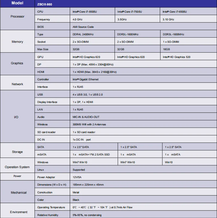 The same goes for testing with Asus’s Strix Z270G Gaming. There are some practical differences in features and even performance, due to differences in the BIOS/firmware, but so far overclocking hasn’t shown any major gaps between modest parts like the Tomahawk and higher end offerings like the Gaming M7.
For Skylake comparisons, I’ve used two different motherboards. First is my standard testbed for Skylake, with Asus’s mainstream Z170-A motherboard. The second board is ASRock’s Z170 Gaming K6 , which supports BCLCK overclocking of non-K processors. This feature was present, then disabled at one point, but now it’s back. That makes Intel’s i5-6400 and i5-6500 potential options for overclocking as well, if you’re willing to go with the ASRock board.
Incidentally, word on the street is that Intel isn’t very happy with ASRock and others for providing this functionality, and some boards that once had non-K overclocking ended up disabling the feature. I definitely wouldn’t count on Z270 boards to support non-K overclocking, but I guess we’ll have to wait and see.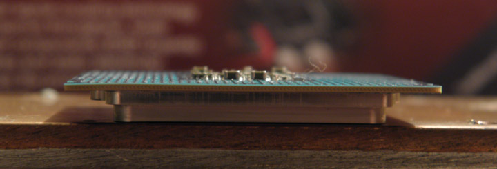 Anyway, the ASRock Gaming K6 using the latest P7.20 BIOS still works with an i5-6400, a $185 true quad-core part , meaning an extra $15 compared to the i3-7350K. That adds a third Skylake comparison point to the overclocking charts.
Overclocking settings
There was a time when overclocking required a certain amount of finesse and skill. These days, you can get 98 percent of the maximum performance with very little thought or effort. Adding faster RAM and manually tweaking timings might be interesting for a small subset of users, but most enthusiasts are content to adjust the CPU multiplier, resulting in 100MHz steps (or 50MHz on some AMD CPUs). This is the approach I took here, tuning the multiplier and voltage and running some stress tests to find a stable result. Here’s the high-level overview, with some additional notes below.
The Skylake chips are pretty straightforward. Both the i7-6700K and i5-6600K managed to run stable at 4.7GHz. 4.8GHz was almost stable, but a few tests would occasionally lock up, even with additional voltage. The i5-6400 is a different beast, where you can’t adjust multiplier but have to tweak the BCLCK, and in the process you need to disable some of the power saving features like SpeedStep and C states. I was able to hit 160MHz BCLCK with a 27X multiplier, yielding a decent 4.3GHz clock speed. There are drawbacks (like idle power, which is about 30W higher than most other Skylake/Kaby Lake CPUs), but it ends up being a very capable chip. It also ends up with the highest overclock, in terms of percent increase over stock—4.3GHz being nearly 40 percent higher than the 2.7-3.3GHz the chip runs at stock.
For the X99 chips, there are more options available, like per-core overclocking on Broadwell-E parts. I decided not to try for the final 1-2 percent performance increase and just apply the same overclock to all cores. I know that in testing, the i7-6950X appears to have three cores that could go higher (they’re typically 5-10C lower during stress testing than the other cores), but that will vary by chip.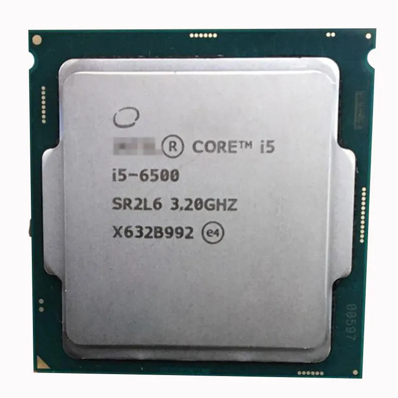
Finally, we have the three Kaby Lake processors. I had hoped to hit 5.0GHz on Kaby Lake, but I only managed that with the i7-7700K. Depending on yields, this could be the result of binning (the best chips become i7-7700K while lesser chips become i7-7700 or i5-7600K for example), or it could just be luck of the draw.
The i3-7350K and i5-7600K both ended up at 4.9GHz, coming up just short of the hallowed 5GHz land of milk and honey. Interestingly, the i3-7350K with an inexpensive cooler (an old Intel boxed air cooler from a Haswell or Ivy Bridge chip, believe it or not) could still run fine at 4.8GHz, which is something to keep in mind. The higher power draw of quad-core parts will require something more, however.
I have to admit to being a bit sad that all three Kaby Lake samples I tested topped out at 4.9 or 5.0GHz. Either I got a bit unlucky, or the 14nm+ process is only good for an extra 200MHz or so with overclocking. With MSI’s board actually shooting for 5.2GHz via auto-overclocking, it got my hopes up. Still, this is the first time I’ve had an Intel chip running at 5.0GHz fully stable. I’ve been stuck in the land of 4.x GHz going back as far as the Pentium 4 days
Intel has added a new feature with Kaby Lake that factors into overclocking—or rather, they brought over a feature from Broadwell-E and Xeon processors. AVX instructions can use more power and create some instability with overclocking, so Intel added an AVX offset multiplier. The values start at 0 and go down (negative), and when the CPU runs AVX instructions the multiplier will drop by the specified amount.
In practice, this didn’t matter on any of the CPUs I benchmarked…except for the i5-7600K, where I set AVX offset to -1 in order to successfully complete y-cruncher without throttling or other errors. Anandtech’s overclocking testing offers a bit more detail on AVX offset, but they weren’t able to surpass a 5.0GHz overclock, either.
Careful, those pins are fragile!
Overall overclocking performance
As with the main Kaby Lake overview, I have limited performance results when it comes to gaming. I’ve done a bit of testing with i7-5930K and confirmed that the increased CPU core counts on Haswell-E and Broadwell-E don’t do much for gaming performance, so I’ll only report gaming performance for the Kaby Lake and Skylake parts, while I’ll show the full suite of CPUs for non-gaming tests.
Here are the non-gaming results—note that this is a gallery of slides, so click the small arrows for the individual results. (If you want to see non-overclocked performance, you’ll have to look at the main Kaby Lake piece, but I’ll discuss the overall performance improvements below.)
Image 1 of 10
What’s the best overclocking chip? If you’re talking about the potential for improved performance, that’s easy: it’s the i5-6400, where performance increases an impressive 35 percent thanks to the 160MHz BCLK. Is it fair to include a non-K CPU in the charts? You can be the judge, but obviously it makes the value proposition for the i3-7350K very questionable. It also explains why Intel doesn’t want to allow BCLCK overclocking on non-K processors, since it eats into the potential market for K-series chips.
For the officially overclockable CPUs, the largest increase in performance is the i5-6600K, improving by nearly 20 percent. The i3-7350K comes next, with a 17 percent improvement. The i5-7600K performance is up 15 percent, followed by the i7-6700K at 11 percent, and finally the i7-7700K at just 8 percent. That’s pretty much what you’d expect from the base clock speeds—the higher the stock clocks, the lower the potential improvement from overclocking.
Looking at the individual performance charts, the three Kaby Lake chips all do great at single-threaded performance, since they have the highest clock speeds and are otherwise the same architecture as Skylake. In other words, if you never want to mess with overclocking, Kaby Lake’s clock speed improvements are a nice little bump, but there’s little new overhead for overclocking, so the year-old Skylake chips can make up for the speed difference.
There are a few tests that clearly favor Intel’s architecture over AMD’s Bulldozer (y-cruncher for example), but AMD’s chips are mostly here as a point of reference—Ryzen will be the real comparison come March. AMD does do pretty well in the VeraCrypt and 7-zip tests, though.
Gaming overclocking performance
Image 1 of 16
I don’t have current gaming results for all of the processors (yet). That allowed me to fit both the stock and OC numbers into a single chart, which gives a nice view of the full range of performance options. And what we learn isn’t too surprising, though the i3-7350K results might raise a few eyebrows. Even at stock, the i3-7350K ends up just 15 percent slower than the fastest overclocked CPU for gaming—in overall performance, at least.
Moving to the individual games, Hitman (DX12) is the best result, followed by Ashes of the Singularity. Both improve performance by 40-50 percent moving from stock i3-7350K to overclocked i7-7700K. Total War Warhammer and Civilization VI also show significant gains, at least compared to the i3-7350K. But if you’re running any decent CPU, including the overclocked i5-6400, the benefits of moving up to a ‘faster’ processor are pretty limited.
There are also plenty of games where your choice of CPU makes virtually no difference, even with a GTX 1080—look at The Division and The Witcher 3, for example, and Deus Ex, Doom (with Vulkan), Far Cry Primal, and Rise of the Tomb Raider aren’t much better. Battlefield 1 single-player also doesn’t need a ton of CPU, though the multiplayer game is a lot more demanding.
Overall, unless you have a relatively slow CPU (like the stock i5-6400 or i3-7350K), overclocking isn’t going to net you a lot of extra performance in games. That’s not too surprising, since even in CPU limited situations we don’t normally see overclocking help by more than 10-15 percent, but if you’re wondering where the bottleneck lies in your gaming PC, look first to the graphics card, second to RAM and storage, and third to your CPU and platform would be my advice—unless you’re running a very old/slow CPU.
Closing thoughts
Kaby Lake is clearly better/faster than Skylake, but while it might be a statistically significant improvement, it’s not generally going to be practically significant—especially for gaming. Overclocking doesn’t really change the story, as the new chips generally get an extra 200-300MHz compared to Skylake, which in practice amounts to 3-4 percent more performance at best—and in games, not even that.
It’s great to see all three chips in the 4.9-5.0GHz range, even without a ton of effort. But will the added performance typically be noticeable? No.
What about the new entry-level K-series chip, the i3-7350K? It’s sort of a cool and novel idea, and it can certainly handle games. However, the price makes it a less attractive option. The i5-6400 with the right motherboard is one obvious alternative, and even if you’re not doing non-K overclocking, I’d generally recommend looking at a Core i5 processor rather than the i3-7350K—the i5-6500 goes for $190 online, and runs about 10-12 percent faster (at stock) than the i5-6400 for example.
The problem with the i3-7350K is that, in pursuit of saving $20 or so (relative to the i5-6500), you’re getting a processor that needs a Z270 motherboard to shine, and in many tasks the additional cores of the i5 will still end up delivering a better overall experience. You could buy an i5-6500 or the new i5-7500, pair that with a less expensive h270/h370 motherboard, and run stock, all for less money than an overclocked i3-7350K plus Z270. In other words, where the Pentium G3258 was interesting primarily thanks to its ultra-budget price, the i3-7350K ends up being far too close to better CPUs to catch my interest.
If you’re not already running Skylake and were thinking about building a new system, short of waiting for AMD’s Ryzen to come out (current ETA is March for retail availability), Kaby Lake gets you another 200-300MHz—stock and overclocked. Don’t forget that the K-series CPUs also need a decent aftermarket heatsink, which can add another $30 to $100 depending on how high-end you want to go.
Overclocking is easier now than it’s ever been, but the potential gains have shrunk to the point where running stock doesn’t mean you give up on a lot of ‘free’ performance.
Jarred’s love of computers dates back to the dark ages when his dad brought home a DOS 2. 3 PC and he left his C-64 behind. He eventually built his first custom PC in 1990 with a 286 12MHz, only to discover it was already woefully outdated when Wing Commander was released a few months later. He holds a BS in Computer Science from Brigham Young University and has been working as a tech journalist since 2004, writing for AnandTech, Maximum PC, and PC Gamer. From the first S3 Virge ‘3D decelerators’ to today’s GPUs, Jarred keeps up with all the latest graphics trends and is the one to ask about game performance.
My ~4000 word long Skylake-X OC Guide
Some time ago I posted a picture of me overclocking my i7-7820X. The post got some resonance and I offered to write down my thoughts on Skylake-X overclocking, as some of you seemed to be interested. Well, here it is! You can download the script in a nice and tidy word file, or you can read this post instead. Feel free to point out mistakes of any kind.
Google Drive link
Skylake-X OC Script by u/aceCrasher
Table of contents:
-
Introduction: What this is and what it isn’t
-
Skylake-X: An architectural deep-dive
-
Basic notes on overclocking
-
Preparation: Before we start
-
Recommended tools
-
Overclocking the cache/mesh
-
Overclocking the memory
-
Overclocking the cores
-
What you can expect: My results
-
My personal Settings
1. Introduction: What this is what it isn’t
First, I am not a professional overclocker or an Intel employee. I overclock for fun in my free time, though I would call myself an enthusiast. I’ve owned a i7-7820X for the last ~4 years and spent much time researching how to overlock it. This includes countless hours of tweaking myself, as well as discussing in forums. My personal experience is limited to LCC dies, but I will include tips for HCC users based on my knowledge from chatting with other overclockers. I don’t take responsibility if you damage your hardware, though I will try to prevent you from doing that to the best of my knowledge. This document includes an overview of the Skylake-X line of processors, their strengths and weaknesses, why I think you should overclock them, what you can expect from overclocking them and finally how to do it. Feel free to disagree on my methods, this is my way of doing it. Let’s get started!
This guide specifically covers the Intel 7th gen Core-X CPUs, meaning 7800X-7980XE. Suggested voltages apply to these chips. The suggested voltages will work on 9th and 10th gen but are possibly unnecessarily high due to their improved manufacturing. All architectural notes and overclocking methods also apply to 9th and 10th gen Core-X CPUs, meaning 9800X-9980XE and 10900X-10980XE.
If you need some motivation, read section 9 first!
2. Skylake-X: An architectural deep-dive
In this part I will cover what Skylake-X series of chips is and what makes the unique in Intel’s lineup, this part is optional, but I highly recommend you read it if you own one of these chips. This section applies to 7th-10th gen Core-X CPUs.
The Core-X family of chips is Intel’s HEDT lineup of CPUs for the desktop, released between 2017 and 2019. It includes 7th, 9th and 10th gen parts. The Core-X family uses the LGA-2066 socket and is exclusive uses the X299 chipset.
All these chips are manufactured on various iterations of the now infamous Intel 14nm node, specifically:
-
14nm+ (7th gen)
-
14nm++ (9th gen)
-
14nm+++ (10th gen)
These chips are not based on the same architecture as the regular Skylake desktop chips, such as the 7700K, 9900K or 10900K. They are derivatives of Intel’s server lineup, repurposed for workstation use. There are 3 different dies in this family, codenamed LCC, HCC and XCC. This stands for low-core-count, high-core-count and extreme-core-count respectively. The X-299 chips only use the LCC and HCC dies. All 6-10 core parts are based on the LCC die (~322mm²), while the 12-18 core parts are based on the HCC die (~484mm²).
The first and major difference between Skylake-X chips and their mainstream counterparts is the core architecture they use. While both are based on Skylake-X, they are not the same. The consumer lineup uses the Skylake-S design, while the HEDT and server lineups use the Skylake-SP design. I will not detail everything that is changed between these designs, only the parts that I think are relevant to consumers.
Skylake-SP cores were first and foremost designed for maximum throughput in compute workloads, which is why Intel added the AVX512 instruction set. These vector instructions offer immense throughput but require high cache bandwidth to not starve the cores. These instructions are almost exclusively used by highly specialized applications and have almost no use to desktop users. If you don’t know what AVX512, you are probably not using it.
A CPUs cache is its fast internal memory, accessed before trying to load Data from DRAM. Skylake-SP has a significantly different cache design compared to Skylake-S:
| Skylake-S | Skylake-SP | |
|---|---|---|
| 32 KB (size), 4-cycle (latency) | L1-D (Data) | 32 KB (size), 4-cycle (latency) |
| 32 KB | L1- (Instruction) | 32 KB |
| 256 KB, 11-cycle | L2 | 1 MB, 11-13-cycle |
| 2 MB/core, 44-cycle, Inclusive | L3 | 1.375 MB/core, 77-cycle, Non-inclusive |
As you can see, the difference lies in the L2 and L3 caches. Intel widened the L2, giving it more capacity and bandwidth. This was done to feed the individual cores in AVX2/AVX512 compute workloads. The L3 was downgraded in return, both in size and latency. It was also changed from being inclusive to being non-inclusive. An inclusive cache necessarily contains everything in the cache underneath it, the benefit being that if something gets removed from the L2, it will still be present in the L3. This was not an option for Skylake-SP because the L2 is so large that the L3 would have to be humungous to store all the L2 data as well. Skylake-SPs L3 is a victim-cache, meaning that stuff evicted from the L1 and L2 gets stored here.
What does this mean for you? If you game on your Skylake-X CPU: quite a bit. The L2 cache is private to each core, so even though an 8-core 7820X has 8 MB of total L2 cache, each individual core can only access 1 MB of it. The L3 however is connected to the mesh and therefore shared between cores. A 7820X has 11 MB total L3 cache, and each core can access the entirety of that. This is relevant because games are a type of workload that has datasets much larger than 1MB, meaning L3 size and latency matters a lot for gaming performance – the upcoming Zen3D chip featuring a larger L3 cache specifically for gaming is good example of this.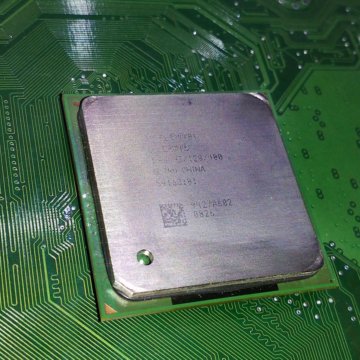
Skylake-X’s comparatively small L3 cache is the reason for its weaker gaming performance at ISO frequency, compared to Skylake-S based chips. Its small L3 cache sized leads to them accessing the DRAM more often, making DRAM latency crucial for increasing Skylake-X gaming performance. More on this later.
The second significant difference between Skylake-S and Skylake-SP based chips are the type of interconnects they use. An interconnect is the part of a chip that connects the cores, L3 cache and the rest of the chip to one another.
Ringbus, Mesh
In a ringbus all the parts are connected to one bi-directional link, this leads to limited power consumption and low latencies, if there are few ring stops. For low core-count CPUs, this is the optimal design. Skylake-S designs like the 7700K or 10900K use a ringbus. The increased number of stops on the 10900K is the reason why a 10900K has inherently higher memory latency than a 7700K at the same DRAM settings.
The mesh connects each core to all its respective neighbors, this leads to higher power draw compared to a ringbus because there are more active links within the chip needing to be powered. This increase in density and power draw leads to Intel’s mesh being clocked lower compared to their ringbus, which results in higher baseline latency within small chips. The mesh’s strength is its scalability. Data can take the shortest route within the chip, meaning that at it beats the ringbus in latency in high core-count chips. The mesh shares a clock domain with the L3 cache, so overclocking the mesh means overclocking the L3 cache too.
A feature unique to Skylake-X is the so called FIVR, the Fully Integrated Voltage Regulator. This is another VRM stage built into the chip itself. You are likely aware of some voltages used in overclocking Intel chips like Vcore (Core), VCCSA (System Agent) or VCCIO (Input-Output). Skylake-X adds another important one to this list: VCCIN. VCCIN is the voltage provided to the chip by the motherboard VRM. The CPU than converts VCCIN to its internal voltages, like Vcore or VCCSA.
All Skylake-X chips come with a Quad-Channel DDR4 memory interface, in contrast to the regular Dual-Channel DDR4 interface found on Intel’s mainstream platforms.
Finally, lets talk about thermal interface materials. All 7th gen Core-X parts are not soldered, instead they use a thermal compound between the die and the IHS. This thermal compound used by Intel is notorious for being terrible. As a response to the widespread criticism regarding this, all 9th gen and 10th gen parts are soldered.
3. Basic Notes on overclocking
In this section I will quickly detail some very basic overclocking information and methods, aimed at absolute beginners. Feel free to skip this part.
When overclocking and testing for stability, don’t change multiple settings at the same time. For example, only increase or decrease one voltage at a time, otherwise you won’t know which change lead to instability afterwards.
Take notes! This is important, document what you are doing, write down temps during testing, what voltage the chip is running at, benchmark scores you are getting, etc. This allows you to spot problems effectively.
Regularly check if performance is increasing between runs, sometimes you achieve higher frequencies, but performance still degrades for some reason. You want to spot this immediately. This is especially important for Skylake-X CPUs, more details later.
4. Preparation: Before we start
Check what kind of motherboard you have. This is important. Skylake-X chips are known for their extreme power draw, especially when overclocked. Your motherboard must be able to handle this amount of power. There are two parts of your mainboard relevant here, the VRM and the CPU power connectors.
Check how many ATX CPU Power connectors your motherboard has. If it only has a single 8-pin connector, you probably shouldn’t overclock at all, or at most a little. You should be fine if it has an 8+4 or 8+8 pin setup.
Next up is the VRM (Voltage Regulator Module), this part of your motherboard controls the voltage fed to your CPU, it converts the 12V coming from your mainboard to VCCIN. The problem here is that it creates heat while doing so, a lot if it when overclocking. A lot of early X299 motherboards from the 7th gen era had terrible VRM heatsinks and are known to overheat when overclocking. I highly recommend watching der8auers video on this topic before you continue. Make sure your motherboards VRM and its cooling is adequate for overclocking.
The next topic is cooling which is immediately brings us to the topic of delidding. Delidding is the process of removing the IHS (Internal Heatspreader) of your CPU and removing the underlying thermal compound with a superior one. This part is relevant to 7th gen chip only. Do not attempt to delid 9th or 10th gen chips, as these are soldered.
If you have a 7th gen chip, I strongly recommend you to delid it. The stock thermal compound used by Intel on these chips is terrible.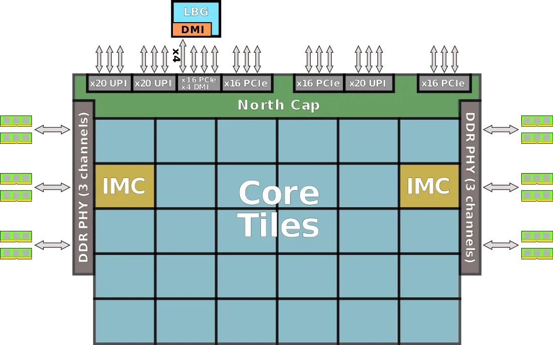 I recommend using der8auers Delid Die Mate X. You can watch his tutorial on using it here. This is worth it if you are serious about overclocking these chips. Only delid if you know what you are doing, or are confident in taking the risk, this is not a trivial process. I recommend Thermal grizzly conductonaut liquid metal thermal paste as a replacement between the die and IHS.
Technically, you can overclock using any cooling system. Considering the immense heat output of this platform though, I would recommend you look into water cooling your chip. We are talking about 200-500W of heat here, use air coolers at your own risk.
Before you start tweaking the chips, make sure that you manually fixate some settings. Leaving them on auto means that you motherboard will change settings without you noticing, this may cause instability without you noticing.
LLC (Load Line calibration) applies additional voltage to the cores when intense load sets in. This counteracts Vdroop (A lowering of voltage when sudden intense load is applied) and prevents the system from crashing on load spikes.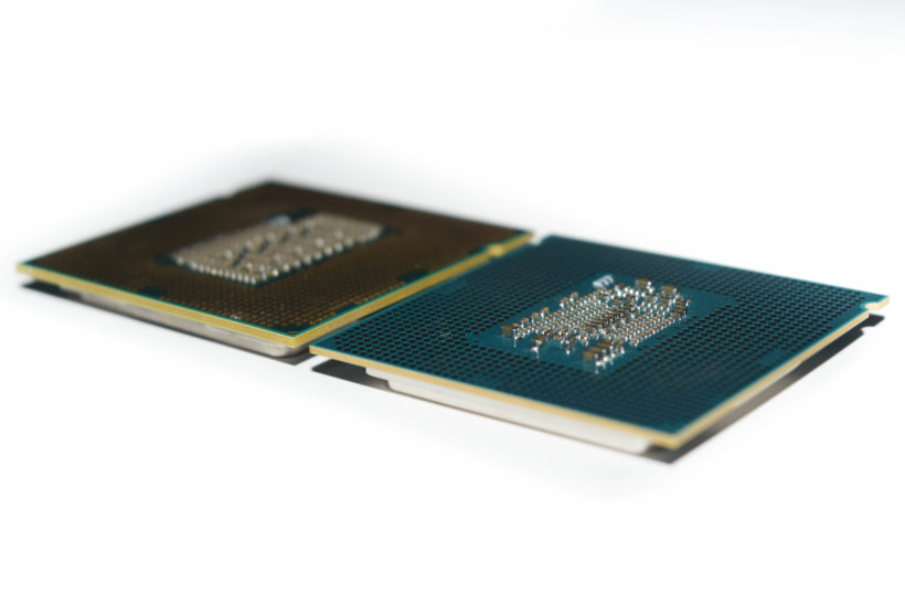 Begin with fixating this at a medium setting, we can modify it later.
Set the CPU Input voltage (VCCIN) to 1.85V for LCC chips and 1.95V for HCC chips, this is a good baseline for overclocking in my experience. This can also be changed later. ASRock X299 boards like to auto-change VCCIN to 2.1V when the users overclocks the CPU, keep an eye on this.
Set VCCSA to 0.900V and VCCIO to 1.100V. This is a good baseline. VCCSA doesn’t need to be increased on Skylake-X in my experience. You might need to raise VCCIO later depending on how aggressively you overclock.
Set uncore-offset to +250mv, this might need to be increased later. If you leave it on auto, your mainboard will raise it by itself when overclocking. Uncore voltage here is analogous to VCCSA in regular Skylake-S chips, which is why we can leave our VCCSA at such a low value.
Set AVX2 offset to -10 and AVX512 offset to -14. I know, these seem extreme, but we will change them later. These settings are only meant to provide a stable baseline.
5. Recommended tools
-
Prime95 for testing stability
-
HCI Memtest for testing RAM/IMC stability
-
HWiNFO64 for monitoring
-
Cinebench for benchmarking performance
-
LinX for testing AVX512 stability
-
Aida64 for measuring DRAM latency
6. Overclocking the cache/mesh
Our first step will be to overclock the L3 cache and mesh of the chip, these share frequency and voltage. I like to start with this because instability in the cache/mesh of the chip can lead to crashes in a wide variety of stress tests. Overclocking this part of the chip brings rich benefits, especially for gaming, as it speeds up the slow L3 as well as reducing memory latency. From here on I will refer to these only as mesh frequency and mesh voltage.
Before you start, measure DRAM latency at stock settings using the Aida64 Cache and Memory Benchmark tool.
You can decide whether you want to use a fixed mesh voltage or adaptive with an offset. I recommend sticking to override when trying to find a stable setting, you can use adaptive later to save energy when idling.
Mesh stock frequency is 2.4GHz on 7th gen, every chip should be able to achieve 3.0GHz, most chips are able to run 3.2GHz, the maximum I consider realistic is 3.5GHz. Aim for at least 3.2GHz if possible.
I recommend a maximum mesh voltage of 1.25V. Scaling falls off above 1.2V in my experience. HCC chips (12-core and above) tend to require ~50mv more mesh voltage compared to LCC chips at the same frequency. Our starting point will be 3GHz at 1.0V. This is a failsafe and should be stable on almost all chips. Test for stability with Prime95 (AVX512+FMA3+AVX2 disabled, Small FTT). Measure DRAM latency, it should have improved compared to stock settings. If Prime95 crashes, increase mesh voltage in 25mV steps. If it is stable, increase mesh frequency by 100MHz.
Some chips require an increase in VCCIO voltage to stabilize high mesh frequencies.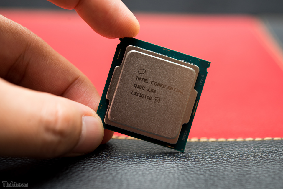 If you run into a brick wall, try raising VCCIO to 1.15V or 1.2V. Try this after increasing mesh voltage. If it doesn’t help, revert to 1.1V.
Another thing you can try to stabilize high mesh frequencies is upping the uncore offset in 100mv steps, though you shouldn’t go higher than 450mv. Try this after increasing mesh voltage. If it doesn’t help, revert.
Do some extended stress testing when you think you have found your final settings. Try Prime95 Small FTTs with and without AVX2/FMA3 enabled. After that run Prime95 custom with 576K FFT size, this will put maximum stress on the uncore. You want your mesh OC to be completely stable before proceeding to the next part.
7. Overclocking the memory
Doing DRAM OC is highly valuable on Skylake-X chips because their small and slow L3 makes them reliant on frequent DRAM access, especially in games. This however is not a DDR4 tuning guide. I will provide CPU related tips for stabilizing high DRAM frequencies, but I won’t explain how to tune the memory itself.
If you are committed to getting the maximum out of your chip, I recommend you study this guide on overclocking DDR4. If memory overclocking is black magic to you, I advise you to activate your memories XMP profile and test for stability only.
The IMC (Integrated Memory Controller) voltage is determined by the uncore-offset, not by System Agent. We set this voltage to +250mv earlier, this should be enough for ~3400MHz DRAM frequency. Try +300mv for 3600MHz, +350mv for 3800MHz and +400mv for 4000MHz. Try raising these as needed when increasing DRAM frequency. I advise against setting more than +450mv. Not all boards can monitor the uncore voltage. If yours can, check it – try to not go higher than 1.35V.
VCCIO might need to be raised at higher DRAM frequencies. Try increasing it from our 1.1V baseline as needed. Don’t go above 1.25V.
If you are looking to buy a RAM Kit for your Skylake-X chip, try to buy one with Samsung B-Die memory chips. There are plenty of guides online that explain how to get these guaranteed. I use a Samsung B-Die Kit myself.
8. Overclocking the cores
Now, finally, the cores. Ill remind you one last time, your mesh and memory settings should be stable at this point, otherwise you will get very frustrated finetuning your core overclock that’s crashing because of some bad mesh or memory setting.
The first thing we will ask ourselves is: do you use any AVX512 workload? If not, skip all the AVX512 parts and set the AVX512 offset to something like -14. You will not encounter these instructions in everyday use unless you use specific software that requires them. You can still tune AVX512 for fun if you want though.
With my method, we are going to use adaptive voltage with offsets. This may rub some people the wrong way but hear me out. Skylake-X runs very hot and with AVX it runs extremely hot. If you use override voltage setup for normal instructions, your AVX2/AVX512 voltages will likely be way too high. Therefore, we use adaptive voltage.
Please note that every piece of silicon is different, the voltages I will suggest here are guidelines, they wont necessarily work just because they worked for someone else.
Our stress test of choice for core overclocking is Prime95 Small FTT, with AVX512/FMA3/AVX2 disabled for now. Testing for a few minutes is fine, you don’t need to let it run for an hour every time.
Let Prime95 run with the given settings and note down what frequency and voltage your chip runs at. You should also note maximum temperature for later reference.
Now increase the CPU multiplier in single steps from your stock all core boost. If your default all core boost was 4GHz, try 41 multi first. Check for stability again. Repeat this until the system becomes unstable. If it does, increase the core voltage offset in 20mv steps until it is stable. Stop this process when core temperature prevents you from raising the voltage offset any further. Temps under 100C are fine for stress testing.
Intel 14nm Skylake chips of every kind, including Skylake-X, can take 1.4V Vcore no problem, but you will never hit this voltage limit because you will always be temperature limited first. So don’t worry about high Vcore damaging your chip.
I will now list some sensible Frequency/Vcore settings for LCC chips. The cooler your chip, the less voltage it needs. These settings are just guidelines, don’t blindly follow them, if your chip needs less: fantastic. If your chip is particularly low quality, it might need more. Most chips should fall within the given ranges. HCC chips need a little more voltage on average to reach the same frequencies.
4400MHz @ 1.080V to 1.140V
4500MHz @ 1.100V to 1.170V
4600MHz @ 1.120V to 1.200V
4700MHz @ 1.150V to 1.220V
4800MHz @ 1.170V to 1.250V
4900MHz @ 1.200V to 1.300V
5000MHz @ 1.250V to 1.320V
Don’t change your core voltage offset after you have found your maximum frequency, we will now proceed to testing AVX2 stability.
Stress test using Prime95 Small FTT with only AVX512 disabled. FMA3 and AVX2 stay enabled this time around. If it is stable, decrease your negative AVX2 offset by 1, meaning that if it was 10 before, set it 9. Stress test with Prime95 again. Repeat this process until you have found the minimum AVX2 offset for the core voltage offset you configured earlier. Don’t change the core voltage offset at this point, you might mess up your overclock for regular instructions.
If you care about AVX512, you can repeat the exact same process with the negative AVX512 offset and Prime95 with AVX512 enabled. You can use LinX as an additional AVX512 stress test that is more burst oriented.
The input voltages we set at the beginning should be sufficient, I have not experienced any gain from increasing them further, even at 5GHz. You can try increasing them my 50mv to see if it helps your chip though.
9. What you can expect: My results
In this section I will provide some benchmarking results from my testing. Each test has been run 3 times and the results have been averaged afterwards. I will compare 4 different profiles.
I would have loved to include some gaming related CPU benchmarks, but since my beloved GTX1080 has recently committed suicide, this is near impossible.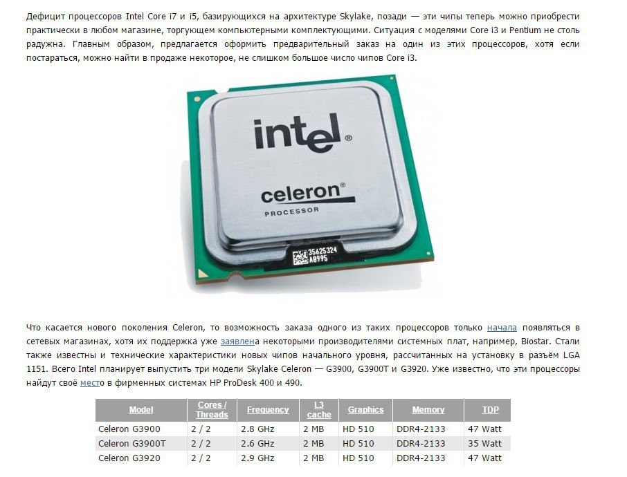 The API Overhead test should be representative of gaming performance.
Components used:
-
i7 7820X
-
Asus X299 Prime-A II
-
4x8GB G.Skill Trident Z Neo 3200CL14
-
Radeon RX560 4GB
-
Custom loop watercooling
-
Super Leadex Platinum 650W PSU
| Profile 1 | Profile 2 | Profile 3 | Profile 4 | |
|---|---|---|---|---|
| CPU-Settings | Stock | Stock | Manual OC | Manual OC |
| RAM-Settings | Stock | XMP | XMP | Manual OC |
| All-core frequency | 4000MHz | 4000MHz | 4900MHz | 4900MHz |
| Mesh/Cache Frequency | 2400MHz | 2400MHz | 3400MHz | 3400MHz |
| DRAM | 2666MHz, 16-18-18-38, CR=2, tRFC=467 | 3200MHz, 14-14-14-34, CR=2, tRFC=561 | 3200MHz, 14-14-14-34, CR=2, tRFC=561 | 4000MHz, 15-16-16-28, CR=1, tRFC=281 |
Graphs:
-
Memory latency
-
Cinebench R15 1T
-
Cinebench R15 nT
-
3DMark API Overhead DX11 1T
-
Geekbench 5 Multi Core
-
Prime95 Large FTT Power Consumption
10. My personal Settings:
WARNING: This section is for reference only, don’t try to just copy and paste these settings!
-
Core ratio: 49
-
Minimum/Maximum Cache ratio: 34
-
Negative AVX2 offset: 5
-
Negative AVX512 offset: 10
-
Load Vcore: 1.199V-1.230V
-
Load Vcore AVX2: 1.050V-1.070V
-
Load Vcore AVX512: 1.045V-1.066V
-
PL1/PL2 Power Limit: 4096W
-
VCCIN: 1.850V
-
VTT: 1.150V
-
VCCSA: 0.900V
-
VCCIO: 1.150V
-
VDIMM: 1.550V
-
Uncore offset: +0.450V
Intel: We ‘Forgot’ to Mention 28-Core, 5-GHz CPU Demo Was Overclocked
Intel’s recent demonstration of a 28-core processor running at 5GHz has certainly stirred the pot here at Computex, particularly because the presentation appeared to imply this would be a shipping chip with a 5.0GHz stock speed. Unfortunately, it turns out that Intel overclocked the 28-core processor to such an extreme that it required a one-horsepower industrial water chiller. That means it took an incredibly expensive (not to mention extreme) setup to pull off the demo. You definitely won’t find this type of setup on a normal desktop PC.
We met with the company last night, and while Intel didn’t provide many details, a company representative explained to us that «in the excitement of the moment,» the company merely «forgot» to tell the crowd that it had overclocked the system. Intel also said it isn’t targeting the gaming crowd with the new chip.
The presentation did take place in front of a crowd of roughly a hundred journalists and a few thousand others, not to mention a global livestream with untold numbers watching live, so perhaps nerves came into play. In the end, Intel claims the whole fiasco is merely the result of a flubbed recitation of pre-scripted lines, with the accidental omission of a single word: «Overclocked.» Maybe that’s the truth, but there’s a lot of room for debate considering how convenient an omission this is.
Intel’s Gregory Bryant began the demo by explaining that the company is working to bring the new chip to market in Q4 of this year, saying, «Without further ado, I would like to present to you a new 28-core processor. «
«
At the end of the demo, which focused heavily on the performance benefits of the 5GHz clock speed, Bryant said, «What’s amazing is that trade-off, this actually being a 5GHz in single-threaded performance frequency and not…having to sacrifice that for this kind of multi-threaded performance, so you’ve got kind of the best of both worlds. So, you guys want to see us productize that thing? Tell you what, we’ll bring that product to market in Q4 this year, and you’ll be able to get it.»
It’s easy to see how some journalists, especially the less tech-savvy ones, could assume that Intel had designed a new 28-core CPU that defies the laws of physics. Given our experience with Intel’s other high core count models, we immediately suspected that the processor was not running at out-of-the-box settings. We know that Intel’s new 10nm process is delayed until possibly late 2019, and pushing a 28-core CPU based on the existing 14nm++ process to 5GHz at stock settings (not to mention on all cores) is simply not feasible.
We were in the crowd live blogging the presentation, but unfortunately, we weren’t close enough to the stage to analyze the test system closely. We reported our suspicions that the company had overclocked the processor, and after the event, we scrutinized the YouTube video and noticed several large insulated tubes coming from the rear of the system (circled in the image above). This is a telltale sign of some type of sub-ambient cooling, such as an expensive liquid chiller or a phase change unit. These units are used to cool the processor to extremely low temperatures, thus allowing it to reach higher clock speeds.
Image 1 of 14
We tracked down the test system the next day and did the full deep dive analysis in our Intel’s 28-Core 5GHz Processor And Test System Breaks Cover article. We learned that Intel had in fact used a water chiller to push the processor to 5GHz, which confirmed our suspicions.
It certainly wasn’t a garden-variety chiller, though. The industrial one-horsepower Hailea HC-1000B can pull a peak of 1000W alone, which is a shocking amount of cooling power for a processor that Intel positioned (by omission) as a chip coming to market at 5GHz. We also learned that the test system required a 1300W power supply, so total system power draw for the demo could stretch up to 2300W. In fact, the hideous amount of juice required to power the demo system prevented our contacts from showing us the performance demo privately: The area we were in simply didn’t have enough dedicated circuits for the task.
We also asked Intel for clarification of the target market for the processor. This 28-core design is likely a variant of Intel’s $10,000 28-core Xeon Platinum Scalable 8180, so it’s certainly a stretch to market it to gamers and enthusiasts. However, Intel’s graphic showed a young person wearing a gaming headset, which implies the processor is for gamers.
However, that isn’t the case. Intel told us the 14nm chip would target the professional workstation market, so it certainly won’t be an X-Series part. Instead, the company hasn’t decided what series the processor will fall into, and might even create another tier for it. We weren’t given a price range for the processor, but it will obviously be far above a normal gamer’s budget.
From Our Core i9-7900X Review
In either case, if you’ve ever used a beefy water chiller or phase-change unit like we regularly do, you’re accustomed to a lot of noise. These units can be extremely loud, so we often use long tubes to run our unit in another room while we test. In its specifications document, Hailea doesn’t list the decibel rating for the industrial water chiller Intel used for the demo, but we learned from our contacts that it easily generates more than 50dBA. According to decibel charts, this is roughly the noise level of a large outdoor air conditioner. Naturally, we would expect some of this noise to bleed over to the presenters’ microphones, thus amplifying it to the crowd, but we couldn’t hear the chiller running during the demo.
We assume Intel placed the chiller in the case underneath the system, so it’s possible the company had to add at least some sound-reducing material inside the box. It’s also possible that the presenters’ unidirectional microphones were good enough to keep the sound of the chiller from coming out over the speaker system, but we think there was probably some form of soundproofing involved.
Companies always try to game demonstrations to some extent. Overall, Intel’s demo setup isn’t too far out of bounds for what we expect from tech demonstrations. There’s always some detail or information left out, or some type of system gaming to squeeze out the best performance under unrealistic scenarios. That applies to many companies the world over, and not «just» Intel.
According to Intel, the accidental omission of a single word skewed the entire demo. For now, the popular sentiment is that Intel is pushing the boundaries of the demo game a bit too far as it competes fiercely with the resurgent AMD. In this case, we think Intel’s demo disaster was a bit of both.
Paul Alcorn is the Deputy Managing Editor for Tom’s Hardware US. He writes news and reviews on CPUs, storage and enterprise hardware.
Topics
Computex
CPUs
Intel Core Socket LGA2066 Processor List-Table
Category: Intel Processor List-Table
Tags: #2066, #Intel_LGA2066, #LGA2066
Description
The LGA 2066 platform was introduced by Intel in 2017. It replaced LGA 2011-3 and was designed primarily for the server segment and high-performance computing systems for home and work. Models are ranked in order of performance from highest to lowest.
List-table of LGA2066 socket processors by performance rating:
| Model | Process family | Cores/Threads | Frequency Turbo | Cache_L2/3 CPUMark | Memory | Video core | TDW Price |
| Core_i9 10980XE | Cascade Lake (14nm) | 18/36 | 3. 0/4.8GHz 0/4.8GHz |
18/25Mb — | DDR4 2933 | — | 165W |
| Core_i9 9980XE | Skylake (14nm) | 18/36 | 3.0/4.4GHz | 18/25Mb — | DDR4 2666 | — | 165W |
| Xeon W_2295 | Cascade Lake (14nm) | 18/36 | 3.0/4.6GHz | 18/25Mb — | DDR4 2933 | — | 165W |
| Core_i9 9960X | Skylake (14nm) | 16/32 | 3.1/4.4GHz | 16/22Mb — | DDR4 2666 | — | 165W |
| Core_i9 9990XE | Skylake (14nm) | 14/28 | 4.0/5.0GHz | 14/19Mb — | DDR4 2666 | — | 255W |
| Core_i9 7980XE | Skylake (14nm) | 18/36 | 2.6/4.4GHz | 18/25Mb — | DDR4 2666 | — | 165W |
| Core_i9 10940X | Cascade Lake (14nm) | 14/28 | 3. 3/4.8GHz 3/4.8GHz |
14/19Mb — | DDR4 2933 | — | 165W |
| Xeon W_2191B | Skylake (14nm) | 18/36 | 2.3/4.3GHz | 18/25Mb — | DDR4 2666 | — | 140W |
| Core_i9 9940X | Skylake (14nm) | 14/28 | 3.3/4.5GHz | 14/19Mb — | DDR4 2666 | — | 165W |
| Xeon W_2275 | Cascade Lake (14nm) | 14/28 | 3.3/4.6GHz | 18/25Mb — | DDR4 2933 | — | 165W |
| Xeon W_2195 | Skylake (14nm) | 18/36 | 2.3/4.3GHz | 18/25Mb — | DDR4 2666 | — | 140W |
| Core_i9 7960X | Skylake (14nm) | 16/32 | 2.8/4.4GHz | 16/22Mb — | DDR4 2666 | — | 165W |
| Core_i9 7940X | Skylake (14nm) | 14/28 | 3. 1/4.4GHz 1/4.4GHz |
14/19Mb — | DDR4 2666 | — | 165W |
| Core_i9 10920X | Cascade Lake (14nm) | 12/24 | 3.5/4.8GHz | 12/19Mb — | DDR4 2933 | — | 165W |
| Xeon W_2265 | Cascade Lake (14nm) | 12/24 | 3.5/4.6GHz | 12/19Mb — | DDR4 2933 | — | 165W |
| Core_i9 9920X | Skylake (14nm) | 12/24 | 3.5/4.5GHz | 12/19Mb — | DDR4 2666 | — | 165W |
| Core_i9 7920X | Skylake (14nm) | 12/24 | 2.9/4.4GHz | 12/17Mb — | DDR4 2666 | — | 165W |
| Xeon W_2170B | Skylake (14nm) | 14/28 | 2.5/4.3GHz | 14/19Mb — | DDR4 2666 | — | 140W |
| Xeon W_2175 | Skylake (14nm) | 14/28 | 2. 5/4.3GHz 5/4.3GHz |
14/19Mb — | DDR4 2666 | — | 140W |
| Core_i9 10900X | Cascade Lake (14nm) | 10/20 | 3.7/4.7GHz | 10/19Mb — | DDR4 2933 | — | 165W |
| Xeon W_2255 | Cascade Lake (14nm) | 10/20 | 3.7/4.7GHz | 10/19Mb — | DDR4 2933 | — | 165W |
| Core_i9 9900X | Skylake (14nm) | 10/20 | 3.5/4.5GHz | 10/19Mb — | DDR4 2666 | — | 165W |
| Core_i9 7900X | Skylake (14nm) | 10/20 | 3.3/4.5GHz | 10/14Mb — | DDR4 2666 | — | 140W |
| Xeon W_2155 | Skylake (14nm) | 10/20 | 3.3/4.5GHz | 14/19Mb — | DDR4 2666 | — | 140W |
| Core_i9 9820X | Skylake (14nm) | 10/20 | 3. 3/4.1GHz 3/4.1GHz |
10/16.5Mb — | DDR4 2666 | — | 165W |
| Xeon W_2155B | Skylake (14nm) | 10/20 | 3.0/4.5GHz | 10/14Mb — | DDR4 2666 | — | 140W |
| Xeon W_2150B | Skylake (14nm) | 10/20 | 3.0/4.5GHz | 10/14Mb — | DDR4 2666 | — | 140W |
| Xeon W_2245 | Cascade Lake (14nm) | 8/16 | 3.9/4.7GHz | 8/16.5Mb — | DDR4 2933 | — | 155W |
| Core_i7 9800X | Skylake (14nm) | 8/16 | 3.8/4.4GHz | 8/16.5Mb — | DDR4 2666 | — | 165W |
| Xeon W_2145 | Skylake (14nm) | 8/16 | 3.7/4.5GHz | 8/11Mb — | DDR4 2666 | — | 140W |
| Core_i7 7820X | Skylake (14nm) | 8/16 | 3. 6/4.5GHz 6/4.5GHz |
8/11Mb — | DDR4 2666 | — | 140W |
| Xeon W_2140B | Skylake (14nm) | 8/16 | 3.2/4.2GHz | 8/11Mb — | DDR4 2666 | — | 140W |
| Xeon W_2235 | Cascade Lake (14nm) | 6/12 | 3.8/4.6GHz | 4/8Mb — | DDR4 2933 | — | 130W |
| Xeon W_2135 | Skylake (14nm) | 6/12 | 3.7/4.5GHz | 6/8Mb — | DDR4 2666 | — | 140W |
| Core_i7 7800X | Skylake (14nm) | 6/12 | 3.5/4.0GHz | 6/8Mb — | DDR4 2400 | — | 140W |
| Xeon W_2133 | Skylake (14nm) | 6/12 | 3.6/3.9GHz | 6/8Mb — | DDR4 2666 | — | 140W |
| Xeon W_2225 | Cascade Lake (14nm) | 4/8 | 4. 1/4.6GHz 1/4.6GHz |
4/8Mb — | DDR4 2933 | — | 105W |
| Xeon W_2125 | Skylake (14nm) | 4/8 | 4.0/4.5GHz | 6/8Mb — | DDR4 2666 | — | 120W |
| Core_i7 7740X | Kaby Lake (14nm) | 4/8 | 4.3/4.5GHz | 1/8Mb — | DDR4 2666 | — | 112W |
| Xeon W_2223 | Cascade Lake (14nm) | 4/8 | 3.6/3.9GHz | 4/8Mb — | DDR4 2666 | — | 120W |
| Xeon W_2123 | Skylake (14nm) | 4/8 | 3.6/3.9GHz | 4/8Mb — | DDR4 2666 | — | 120W |
| Core_i5 7640X | Kaby Lake (14nm) | 4/4 | 4.0/4.2GHz | 1/6Mb — | DDR4 2666 | — | 112W |
| Xeon W_2104 | Skylake (14nm) | 4/4 | 3. 2/-GHz 2/-GHz |
4/8Mb — | DDR4 2400 | — | 120W |
| Xeon W_2102 | Skylake (14nm) | 4/4 | 2.9/-GHz | 4/8Mb — | DDR4 2400 | — | 120W |
Kaby Lake VS Skylake
Content
- 1 4K video
- 2 Thunderbolt 3.0 and USB 3.1
- 3 Higher clock speeds
- 4 Speed comparison
- 5 Optan Support
- 6 PCIe lanes
- 7 Final verdict
Intel introduced Kaby Lake in the second half of 2016 as a direct successor to the popular Skylake processor.
With Kaby Lake, Intel broke the tick-tock cycle of six generations. On the tick, Intel will launch a processor with a new design, and on the «tock» its optimized and improved version will be presented. However, Kaby Lake was an improvement on Skylake, which in turn improved the 5th Gen Broadwell processor.
Let’s see how they fit together. Let the Skylake vs Cuby Lake match begin!
4K video
One of the main differences between Skylake 6th Gen and Kaby Lake 7th Gen is that Kaby Lake processors come with built-in HEVC codec support for 4K video. These processors also delegate most of the 4K video tasks to the graphics cards, which means your laptop will use significantly less battery when playing 4K video.
Kaby Lake processors support VP9, a 4K video codec developed by Google in response to HEVC. In addition, they support the HDCP 2.2 standard. HDCP (High-bandwidth Digital Content Protection) is designed to prevent unauthorized copying of digital content.
Finally, Kaby Lake processors offer much better performance in the 3D graphics department. This means higher frame rates, better resolution, and a better gaming experience across the board. In testing, Intel ran Overwatch on a Dell XPS 13 laptop running a Kaby Lake processor. He managed to achieve a rather impressive (considering the characteristics of the laptop) resolution of 1280 x 720 at 30 frames per second and at medium graphics settings.
Thunderbolt 3.0 and USB 3.1
Kaby Lake processors also offer improvements in this area. With second-generation USB 3.1 support, Kaby Lake processors offer transfer speeds of up to 10 GB/s (5 GB/s was the limit for Skylake processors). In addition, Kaby Lake processors have built-in third-generation support for Intel’s own Thunderbolt.
Computers equipped with Kaby Lake processors can have up to 14 USB ports (2.0 and 3.0) and a trio of PCIe 3.0 storage ports. Of course, in order to take full advantage of Kaby Lake processors, appropriate motherboards are needed.
Higher clock speeds
Considering the fact that Kaby Lake is just an optimized version of Skylake, Intel relies solely on tweaks and improvements to increase performance and speed up the processor. The results are not that impressive, although they are noticeable. However, Kaby Lake processors offer superior performance in the 3D graphics department, especially on mobile devices.
Intel offers Kaby Lake processors in two main designations, Y and U. The Y models now replace the m-designated Skylake models, but only in the i5 and i7 sections. The M designation remains for i3 processors. This makes it impossible to know if you bought an m/Y or i5 class U5 processor without reading its full name.
Speed Comparison
The m3-6Y30 Skylake processor has a base frequency of 900 MHz and a turbo of 2.2 GHz. The M3-7Y30 Kaby Lake typically runs at 1GHz and the turbo at 2.6GHz. Skylake m5-6Y74 operates at 1.2GHz and reaches turbo speed at 2.7GHz. The Kaby Lake i5-6Y74 runs at 1.2GHz while the turbo runs at 3.2GHz. The Skylake M7-6Y75 typically runs at 1.2GHz, turbo at 3.1GHz. On the other hand, the Kaby Lake i7-7Y75 starts at 1.3GHz and goes up to 3.6GHz.
Skylake i5-6200U base speed is 2.3GHz and turbo is 2.8GHz. Its Kaby Lake counterpart (i5-7200U) operates at 2.5 GHz, and Turbo at 3.1 GHz. The base speed of the Skylake i7-6500U is 2.5GHz, with a turbo speed of 3.1GHz. On the other hand, the Kaby Lake i7-7500U has a base speed of 2. 7GHz and a turbocharger of 3.5GHz.
Optane Support
Another major difference between 6th Gen Skylake processors and 7th Gen Kaby Lake processors is that the latter support the innovative Optane memory. Intel is adopting the concept of an SSD that plugs directly into the motherboard. It uses M.2 slots and is not compatible with Sunrise Point 100 series chipsets. Likewise, if you install a Skylake chip on a Union Point 200 series chipset, you still won’t be able to use Optane.
PCIe lanes
The number of PCIe lanes also improved from Skylake to Kaby Lake. While both processors can have up to 16 PCIe 3.0 from the processor, the seventh generation Kaby Lake models can support up to 24 lanes from the Platform Controller Hub (PCH). This brings the total number of PCIe lanes supported by Kaby Lake chips to 40.
Final Verdict
Despite a significant improvement over the sixth generation, the seventh generation Kaby Lake processors are simply not convincing enough to sway casual users already running machines based on skylake.
Native 4K video support, improved 3D graphics, and higher clock speeds may be attractive enough for gamers and media enthusiasts, but they mean little to the general public. The same goes for Optane support and a slightly increased number of PCIe lanes.
Skylake — frwiki.wiki
Skylake i7-6700K processor, top view
Skylake i7-6700K processor in perspective
Skylake is a microarchitecture of x86 processors from Intel , which follows the Haswell20 microarchitecture starting from August 20, .
With this new microarchitecture, Intel is abandoning its traditional ticking strategy. Indeed, the firm had some difficulty in moving to 14nm engraving and is still lagging behind in 10nm engraving. Thus, this architecture is available in many more families than usual.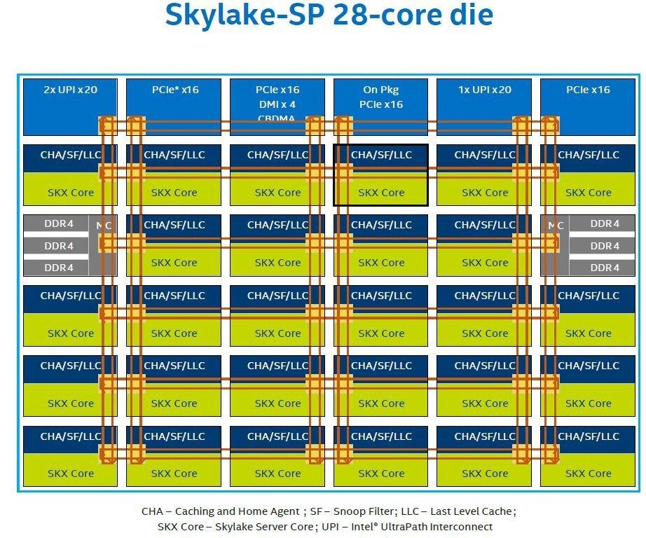
The 10 nm engraved Cannon Lake microprocessor family is scheduled for 2018 and will always be based on the Skylake microarchitecture.
Intel, 10 nm, discovers extreme ultraviolet lithography replacing the traditional argon fluoride immersion laser lithography process at 193 nm .
Thus, the chronology of the listed families of microprocessors is as follows:
- Haswell micro-architecture :
- Haswell processor family engraved in 22 nm since
- Broadwell engraved family 14 nm since
- Skylake microarchitecture:
- Skylake family engraved 14 nm since
- Kaby Lake engraved family 14 nm since
- Coffee Lake or «Kaby Lake Refresh» family engraved 14 nm since
- Cannon Lake family engraved 10 nm since but abandoned late 2019
Summary
- 1 Key features
- 2 changes announced
-
3 Family Skylake — 6 — e generation — 14 nm
- 3.
 1 Notebook processors
 - 3.2 Desktop Processors
- 3.3 X-series processors (Skylake-X)
- 3.
-
4 Family Kabi lake — 7 — e generation — 14 nm
- 4.1 Notebook processors
- 4.2 Desktop Processors
- 4.3 X-series processors (Kaby Lake-X)
-
5 Family Coffee Lake — 8- e generation — 14 nm
- 5.1 Notebook processors
- 5.2 Desktop Processors
- 6 Graphics support
- 7 family Cannon Lake
- 8 links
Main characteristics
- Skylake microprocessor family requires LGA 1151 socket.
- The graphics part evolves with this microarchitecture: The Skylake microprocessor family includes a ninth generation graphics core that supports DirectX 12, OpenGL 4.4 and OpenCL 2.0.
Announced Changes
Intel changes its so-called tick-tock evolution model, alternating engraving changes with a fixed architecture, and then architectural changes with unchanged engraving accuracy. This shows that difficulties appear with engravings around 15 nm , currently requires a three-phase approach: P rocess (fine engraving) rchitecture (new nanocircuits), which mainly aims at new functions, and a third and new stage: O ptimization, which seeks to improve performance, hence the name PAO (not related to the acronym for desktop publishing).
Skylake family — 6 —
e generation — 14 nm
Notebook Processors
When the first 6th generation processors were released, Intel announced a 10% to 15% % performance increase over the previous generation.
| Family | Surname | Number of cores / threads | Normal frequency | Turbo frequency | GPU | TDP | TDP up | TDP down | Presentation | Relative performance |
|---|---|---|---|---|---|---|---|---|---|---|
| Celeron | 3855U | 2/2 | 1. 6 GHz 6 GHz
|
N/A | HD 510 | 15 W | 10 W | Q4 2015 | 0.45 | |
| 3955U | 2.0 GHz | |||||||||
| G3900E | 2.4 GHz | 35 W | Q1 2016 | 0.70 | ||||||
| G3902E | 1.6 GHz | 25 W | ||||||||
| Pentium | 4405Y | 2/4 | 1.5 GHz | HD 515 | 6 W | 4.5 W | Q3 2015 | 0.53 | ||
| 4405U | 2.1 GHz | HD 510 | 15 W | 10 W | 0.78 | |||||
| Intel Core M3 | 6Y30 | 2/4 | 0.9 GHz | 2.2 GHz | HD 515 | 4. 5 W 5 W
|
7W | 3.8 W | ||
| Intel Core M5 | 6Y54 | 1.1 GHz | 2.7 GHz | 3.5 W | 0.85 | |||||
| 6Y57 | 2.8 GHz | |||||||||
| Intel Core M7 | 6Y75 | 1.2 GHz | 3.1 GHz | 0.91 | ||||||
| Intel Core i3 | 6100U | 2.3 GHz | N/A | HD 520 | 15 W | 7.5 W | 1 | |||
| 6157U | 2.4 GHz | Iris 550 | 28 W | 23 W | Q3 2016 | |||||
| 6167U | 2.7 GHz | Q3 2015 | ||||||||
| 6100H | HD 530 | 35 W | 1.08 | |||||||
| Intel Core i5 | 6200U | 2. 3 GHz 3 GHz
|
2.8 GHz | HD 520 | 15 W | 7.5 W | 1.03 | |||
| 6300U | 2.4 GHz | 3.0 GHz | 1.13 | |||||||
| 6260U | 1.8 GHz | 2.9 GHz | Iris 540 | 9.5 W | ||||||
| 6360U | 2.0 GHz | 3.1 GHz | 1.30 | |||||||
| 6267U | 2.9 GHz | 3.3 GHz | Iris 550 | 28 W | 23 W | |||||
| 6287U | 3.1 GHz | 3.5 GHz | ||||||||
| 6300HQ | 4/4 | 2.3 GHz | 3.2 GHz | HD 530 | 45 W | 35 W | 1.56 | |||
| 6350HQ | Iris Pro 580 | Q1 2016 | ||||||||
| 6440HQ | 2. 6 GHz 6 GHz
|
3.5 GHz | HD 530 | Q3 2015 | 1.74 | |||||
| Intel Core i7 | 6500U | 2/4 | 2.5 GHz | 3.1 GHz | HD 520 | 15 W | 7.5 W | 1.14 | ||
| 6600U | 2.6 GHz | 3.4 GHz | 25 W | 1.26 | ||||||
| 6560U | 2.2 GHz | 3.2 GHz | Iris 540 | 9.5 W | ||||||
| 6650U | 2.2 GHz | 3.4 GHz | ||||||||
| 6660U | 2.4 GHz | 3.4 GHz | Q1 2016 | |||||||
| 6567U | 3.3 GHz | 3.6 GHz | Iris 550 | 28 W | 23 W | Q3 2015 | 1.45 | |||
| 6700HQ | 4/8 | 2. 6 GHz 6 GHz
|
3.5 GHz | HD 530 | 45 W | 35 W | Q3 2015 | 2.10 | ||
| 6820HK | 2.7 GHz | 3.6 GHz | 2.35 | |||||||
| 6820HQ | 2.28 | |||||||||
| 6920HQ | 2.9 GHz | 3.8 GHz | 2.50 | |||||||
| 6770HQ | 2.6 GHz | 3.5 GHz | Iris Pro 580 | Q1 2016 | ||||||
| 6870HQ | 2.7 GHz | 3.6 GHz | ||||||||
| 6970HQ | 2.8 GHz | 3.7 GHz |
Desktop processors
| Family | Surname | Number of cores / threads | Normal frequency | Turbo frequency | GPU | TDP | Presentation |
|---|---|---|---|---|---|---|---|
| Intel Celeron | G3900 | 2/2 | 2. 8 GHz 8 GHz
|
N/A | HD 510 | 51 W | Q3 2015 |
| G3920 | 2.9 GHz | ||||||
| Intel Pentium | G4400 | 3.3 GHz | 47 W | ||||
| G4500 | 3.5 GHz | HD 530 | |||||
| G4520 | 3.6 GHz | ||||||
| Intel Core i3 | 6100 | 2/4 | 3.7 GHz | 51 W | |||
| 6100T | 3.2 GHz | 35 W | |||||
| 6300 t | 3.3 GHz | ||||||
| 6300 | 3.8 GHz | 51 W | |||||
| 6320 | 3.9 GHz | ||||||
| Intel Core i5 | 6400 | 4/4 | 2.7 GHz | 3.3 GHz | 65 W | ||
| 6400 t | 2. 2 GHz 2 GHz
|
2.8 GHz | 35 W | ||||
| 6500 | 3.2 GHz | 3.6 GHz | 65 W | ||||
| 6500 t | 2.5 GHz | 3.1 GHz | 35 W | ||||
| 6600 | 3.3 GHz | 3.6 GHz | 65 W | ||||
| 6600 t | 2.7 GHz | 3.5 GHz | 35 W | ||||
| 6600 K | 3.5 GHz | 3.9 GHz | 91 W | ||||
| Intel Core i7 | 6700 | 4/8 | 3.4 GHz | 4.0 GHz | 65 W | ||
| 6700 t | 2.8 GHz | 3.6 GHz | 35 W | ||||
| 6700 K | 4.0 GHz | 4.2 GHz | 91 W | ||||
| 6785R | 3.3 GHz | 3.6 GHz | 65 W |
X-series processors (Skylake-X)
The X-series processors are the most powerful processors on the market, designed for professional use where significant processing power is required. These processors do not have an integrated GPU.
| Family | Surname | Number of cores / threads | Normal frequency | Turbo frequency | GPU | TDP | Issue date |
|---|---|---|---|---|---|---|---|
| Intel Core i7 | 7800X | 6/12 | 3.50 GHz | 4.00 GHz | No integrated graphics processor | 140 W | Q3 2017 |
| 7820X | August 16 | 3.60 GHz | 4.30 GHz | ||||
| Intel Core i9 | 7900X | 10/20 | 3.30 GHz | 4.30 GHz | |||
| 7920X | December 24 | 2.90 GHz | 4.30 GHz | ||||
| 7940X | 14/28 | 3.10 GHz | 4.30 GHz | 165 W | |||
| 7960X | 16/32 | 2. 80 GHz 80 GHz
|
4.20 GHz | ||||
| 7980XE | 18/36 | 2.60 GHz | 4.20 GHz |
Kabi lake family — 7 —
e generation — 14 nm
Please note that these processors are only supported by Microsoft under Windows 10. In Windows 7 and 8.1, they will not be subject to the security update.
Notebook processors
When the first processors were released 7-th generation , Intel announced a performance increase of at least 15 % over the previous generation.
| Family | Surname | Number of cores / threads | Normal frequency | Turbo frequency | GPU | TDP | TDP up | TDP down | Presentation | Relative performance |
|---|---|---|---|---|---|---|---|---|---|---|
| Celeron | 3865U | 2/2 | 1. 8 GHz 8 GHz
|
N/A | HD 610 | 15 W | 10 W | Q1 2017 | ? | |
| 3965U | 2.2 GHz | |||||||||
| Pentium | 4415U | 2/4 | 2.3 GHz | 0.82 | ||||||
| 4410Y | 1.5 GHz | HD 615 | 6 W | 4.5W | ? | |||||
| Intel Core i3 | 7Y30 | 2/4 | 1.0 GHz | 2.6 GHz | 4.5 W | 7W | 3.5 W | Q3 2016 | 0.92 | |
| 7Y32 | 1.1 GHz | 3.0 GHz | 3.75 W | Q2 2017 | ||||||
| 7100U | 2.4 GHz | N/A | HD 620 | 15 W | 7.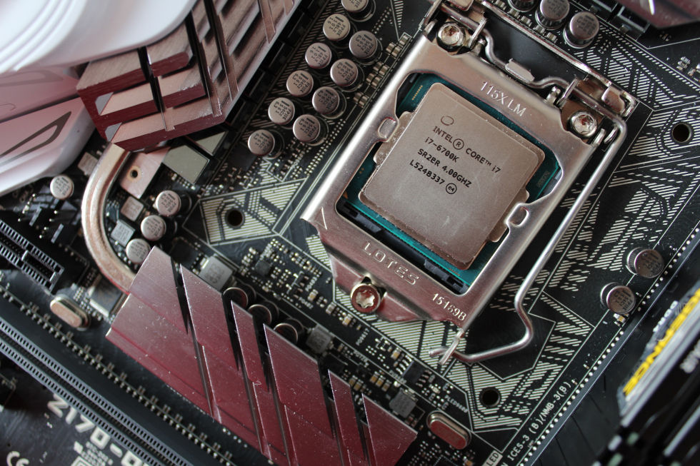 5 W 5 W
|
Q3 2016 | one | |||
| 7130U | 2.7 GHz | Q2 2017 | ||||||||
| 7167U | 2.8 GHz | Iris Plus 650 | 28 W | 23 W | Q1 2017 | |||||
| 7100H | 3.0 GHz | HD 630 | 35 W | 1.22 | ||||||
| Intel Core i5 | 7Y54 | 1.2 GHz | 3.2 GHz | HD 615 | 4.5 W | 7W | 3.5W | Q3 2016 | 1 | |
| 7Y57 | 3.3 GHz | Q1 2017 | ||||||||
| 7200U | 2.5 GHz | 3.1 GHz | HD 620 | 15 W | 25 W | 7.5 W | Q3 2016 | 1.21 | ||
| 7300U | 2.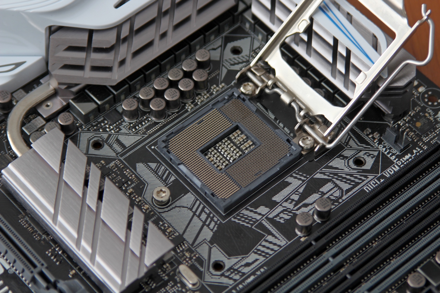 6 GHz 6 GHz
|
3.1 GHz | Q1 2017 | 1.31 | ||||||
| 7260U | 2.2 GHz | 3.4 GHz | Iris Plus 640 | 9.5 W | 1.49 | |||||
| 7360U | 2.3 GHz | 3.6 GHz | 1.56 | |||||||
| 7267U | 3.1 GHz | 3.5 GHz | Iris Plus 650 | 28 W | 23 W | 1.37 | ||||
| 7287U | 3.3 GHz | 3.7 GHz | ||||||||
| 7300HQ | 4/4 | 2.5 GHz | 3.5 GHz | HD 630 | 45 W | 35 W | 1.75 | |||
| 7440HQ | 2.8 GHz | 3.8 GHz | 2 | |||||||
| Intel Core i7 | 7Y75 | 2/4 | 1. 3 GHz 3 GHz
|
3.6 GHz | HD 615 | 4.5 W | 7W | 3.5 W | Q3 2016 | 1 |
| 7500U | 2.7 GHz | 3.5 GHz | HD 620 | 15 W | 25 W | 7.5 W | 1.35 | |||
| 7600U | 2.8 GHz | 3.9GHz | Q1 2017 | 1.45 | ||||||
| 7560U | 2.4 GHz | 3.8 GHz | Iris Plus 640 | 9.5 W | 1.53 | |||||
| 7660U | 2.5 GHz | 4.0 GHz | 1.58 | |||||||
| 7567U | 3.5 GHz | Iris Plus 650 | 28 W | 23 W | 1.68 | |||||
| 7700HQ | 4/8 | 2.8 GHz | 3.8 GHz | HD 630 | 45 W | 35 W | 2.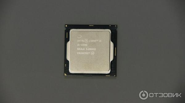 31 31
|
|||
| 7820HK | 2.9 GHz | 3.9 GHz | 2.60 | |||||||
| 7820HQ | ||||||||||
| 7920HQ | 3.1 GHz | 4.1 GHz |
Desktop processors
| Family | Surname | Number of cores / threads | Normal frequency | Turbo frequency | GPU | TDP | Presentation |
|---|---|---|---|---|---|---|---|
| Intel Pentium | G4560T | 2/4 | 2.9 GHz | N/A | HD 610 | 35 W | Q4 2016 |
| G4620 | 3.7 GHz | HD 630 | 51 W | ||||
| G4600 | 3.6 GHz | ||||||
| G4600T | 3.0 GHz | 35 W | |||||
| Intel Core i3 | 7101E | 2/4 | 3.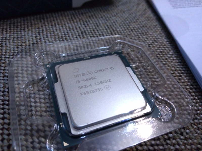 9 GHz 9 GHz
|
54 W | |||
| 7100T | 3.4 GHz | 35 W | |||||
| 7100 | 3.9 GHz | 51 W | |||||
| 7350 thousand | 4.2 GHz | 60 W | |||||
| 7320 | 4.1 GHz | 51 W | |||||
| 7300 | 4.0 GHz | ||||||
| 7300 t | 3.5 GHz | 35 W | |||||
| Intel Core i5 | 7400 t | 4/4 | 2.4 GHz | 3.0 GHz | |||
| 7400 | 3.0 GHz | 3.5 GHz | 65 W | ||||
| 7500 | 3.4 GHz | 3.8 GHz | |||||
| 7500 t | 2.7 GHz | 3.3 GHz | 35 W | ||||
| 7600 t | 2.8 GHz | 3.7 GHz | |||||
| 7600 K | 3.8 GHz | 4. 2 GHz 2 GHz
|
91 W | ||||
| 7600 | 3.5 GHz | 4.1 GHz | 65 W | ||||
| Intel Core i7 | 7700 | 4/8 | 3.6 GHz | 4.2 GHz | |||
| 7700 t | 2.9 GHz | 3.8 GHz | 35 W | ||||
| 7700 KB | 4.2 GHz | 4.5 GHz | 91 W |
X-series processors (Kaby Lake-X)
This is a series of high performance desktop processors. Not to be confused with Skylake-X
| Family | Surname | Number of cores / threads | Normal frequency | Turbo frequency | GPU | TDP | Presentation |
|---|---|---|---|---|---|---|---|
| Intel Core i5 | 7640X | 4/4 | 4.0 GHz | 4.2 GHz | No integrated graphics processor | 112 W | Q3 2017 |
| Intel Core i7 | 7740X | 4/8 | 4. 3 GHz 3 GHz
|
4.5 GHz |
Family Coffee lake — 8th —
th th generation — 14nm
In Intel announced that the release of the 8-th generation will be implemented in stages, with the first mobile processors demonstrating the architecture in the Kaby Lake Refresh version, and office processors appearing in early 2018 with the new Coffee Lake architecture.
Notebook processors
The main novelty of the new mobile processors 8th th generation — gateway to all these 4 cores instead of two hearts. This allows, after several optimizations, to increase performance by almost 40%. When moving to 4 cores, Intel was forced to reduce the operating frequencies in order to provide power consumption of 15 watts.
| Family | Surname | Number of cores / threads | Normal frequency | Turbo frequency | GPU | TDP | TDP up | TDP down | Presentation | Relative performance |
|---|---|---|---|---|---|---|---|---|---|---|
| Intel Core i3 | 8121U | 2/4 | 2. 2 GHz 2 GHz
|
N/A | UHD 610 | 15 W | N/A | 10 W | Q1 2018 | 1 |
| 8130U | 2.2 GHz | 3.4 GHz | ||||||||
| Intel Core i5 | 8250U | 4/8 | 1.6 GHz | 3.4 GHz | UHD 620 | 15 W | 25 W | 10 W | Q3 2017 | 1.75 |
| 8350U | 1.7 GHz | 3.6 GHz | 1.98 | |||||||
| Intel Core i7 | 8550U | 4/8 | 1.8 GHz | 4.0 GHz | UHD 620 | 15 W | 25 W | 10 W | Q3 2017 | 1.86 |
| 8650U | 1. 9 GHz 9 GHz
|
4.2 GHz | 2.08 |
Desktop processors
The main improvement of Coffee Lake processors compared to Kabylake is the increase in the number of cores, as in mobile versions. I3s go from 2c/4t to 4c/4t, i5s from 4c/4t to 6c/6t, and i7s from 4c/8t to 6c/12t (c=core, t=thread).
| Family | Surname | Number of cores / threads | Normal frequency | Turbo frequency | L3 cache | GPU | TDP | connector | Presentation | Relative performance |
|---|---|---|---|---|---|---|---|---|---|---|
| Intel Core i3 | 8100 | 4/4 | 3.6 GHz | N/A | 6 MB | UHD 630 | 65 W | LGA 1151 | Q4 2017 | 1 |
| 8350 thousand | 4. 0 GHz 0 GHz
|
8 MB | 91 W | 1.13 | ||||||
| Intel Core i5 | 8400 | 6/6 | 2.8 GHz | 4.0 GHz | 9 MB | 65 W | 1.45 | |||
| 8600 K | 3.6 GHz | 4.3 GHz | 9 MB | 95 W | 1. 58 58
|
|||||
| Intel Core i7 | 8700 | 6/12 | 3.2 GHz | 4.6 GHz | 12 MB | 65 W | 1.88 | |||
| 8700 K | 3.7 GHz | 4.7 GHz | 12 MB | 95 W | 2 |
Graphics support
To use the Skylake graphics on Linux, at least:
- Linux 4.3
- Mesa 11.0.4
- Intel xf86 video driver 2.