[Beginner Guide] What Is PCIe? What Is It Used for?
PAGE CONTENT:
- 1. What Is PCIe
- 2. What Is PCIe Used for
- 3. Different Types of PCIe
What Is PCIe
PCIe stands for Peripheral Component Interconnect Express, often abbreviated as PCI-e, PCIe, or PCI Express; all are the same. PCI Express is a popular high-speed serial computer expansion bus standard that supersedes other legacy standards such as PCI, PCI-X, and AGP.
Compared to PCI, which applies parallel communication, PCIe uses a serial link connection architecture that utilizes a point-to-point topology, which makes PCIe more reliable, faster overall, and less expensive to produce than the PCI bus. Therefore, most motherboards and computers today are configured with PCI-e slots for expandability capabilities.
What Is PCIe Used for
The purpose of using PCIe is to achieve significantly improved system throughput, scalability, and flexibility at a lower cost.
Due to its robust scalability, PCIe supports devices including graphics cards, solid-state drives (PCIe interface), wireless network cards, wired network cards, sound cards, video capture cards, PCIe to M.2 interface, PCIe to USB interface, PCIe Transfer Type-C interface, etc.
PCIe not only has a high transfer rate but is also good in compatibility. It is compatible with PCI at the software level, version upgrade, backward compatible with PCI software, and supports hot plug.
Different Types of PCIe
The PCIe standard is future-proof and continues to evolve to provide systems with higher throughput. Currently, the PCIe standard has developed from the first generation to the sixth generation, and connection speeds double with each new generation.
The throughput of the PCIe 1.0is 2.5Gbps, the PCIe 2.0 reaches 5.0Gbps, and the latest PCIe3.0 standard supports a rate of 8.0Gbps. Most current processors, computers, and motherboards support PCIe Gen 3 architecture, while newer applications require PCIe 4.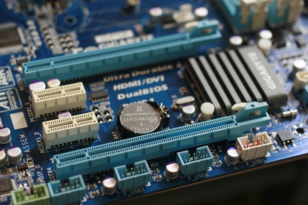 0 performance speeds.
Now the PCI-E slot has become the main expansion slot on the motherboard. And it basically focuses on PCI-E x16/x8/x4/x1 four types.
- PCI-E x16: The x16 slot is 89mm in length, has 164 pins, and has a bayonet outside the motherboard. The slot has excellent compatibility and can be backward compatible with x1/x4/x8 level devices, which is the universal slot of PCI-E.
- PCI-E x8: The x8 slot is 56mm long and has 98 pins. For compatibility, some PCI-E x8 slots are processed into the form of PCI-E x16 slots, but only half of the data pins are valid. That is to say; the actual bandwidth is only half that of a real PCI-E x16 slot.
- PCI-E x4: The length of the PCI-E x4 slot is 39mm, which is also realized by reducing the data pins based on the PCI-E x16 slot. However, like the PCI-E x8 slot, most PCI-E x4 slots are now in the form of PCI-E x16 or x8 slots or expanded to M.
 2 interfaces for compatibility.
 - PCI-E x1: The length of the slot is the shortest, only 25mm. The motherboard chip usually provides the bandwidth of the PCI-E x1 slot. It is mainly used for independent network cards, independent sound cards, USB 3.0/3.1 expansion cards, etc. to the PCI-E x1 slot.
What is PCIe? | TI.com Video
- TI Training home
- PCIe
- What is PCIe?
PCIe
Hello and welcome to TI Precision Labs. In this series, we’re going to discuss Peripheral Component Internet Connect Express, more commonly known as PCIe. PCIe is a motherboard expansion bus standard introduced in 2003 to enable high speed serial communication between the CPU and its peripheral components.
Today, it has become the primary motherboard expansion bus standard and a popular communication method for many other on board applications. Let’s explore how this high speed interface developed and how it works.
The predecessor to PCIe is PCI. The PCI bus existed on many motherboards in the 90s, along with a few other expansion bus technologies. Motherboard expansion bus standards are designed for communication between the CPU and devices plugged into the motherboard’s expansion slots.
Initially, all expansion bus standard used a parallel bus, which means that data is sent and received over multiple channels. Initially, all expansion bus standards used the parallel bus, which means that data is sent and received over multiple channels.
At the time of its introduction in 2003, the PCIe serial bus standard was meant to replace these older parallel buses to enable a higher data rate and to simplify system design. In 2003, the PCIe standard was defined by the PCI Sig organization. Since then, the PCIe standard has iteratively improved over time to accommodate the latest bandwidth needs of modern computers.
This year, in 2021, the PCIe 6.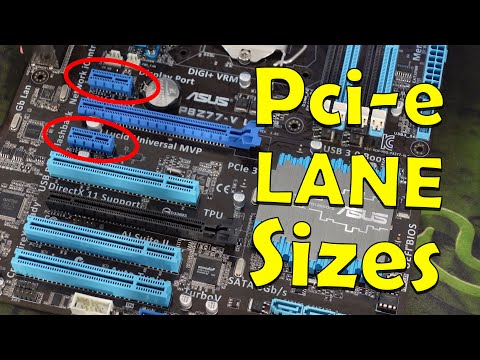 0 specification will be introduced, enabling 64 giga transfers per second, or 64 gigabits per second per link. One unique feature of the PCIe standard is the ability to increase the number of lanes from 1 to up to 32 lanes to increase its throughput, a feature inspired by its parallel bus predecessor.
A PCIe 6.0 link that is 16 lanes wide would have a data rate of 128 gigabytes per second, which is extremely fast by today’s standards. PCIe communication is hierarchical, meaning there is a single source through which all the data passes, which is the root complex. The information passes to the root complex from multiple PCIe endpoints.
Let’s examine in detail how PCIe initializes and communicates over a typical link such as the one highlighted here. Here we have a diagram containing devices that are common in a PCIe link. A root complex is the interface between the system CPU and memory and the rest of the PCIe structure. The root complex is either integrated into the CPU directly, or is external to the CPU as a discrete component.
A repeater is a signal conditioning device. For more information regarding signal conditioners, please refer to the «What is a signal conditioner?» video. Repeaters can fall into two categories. Retimers and redrivers. Both are common PCIe components used to maintain signal quality of high speed links.
In our example, we’ll be using a PCIe 4.0 compliant retimer. An endpoint is a general term for a PCIe end component. This could represent many different types of PCIe devices. In our case, let’s assume that the endpoint is a graphics processing unit, or GPU.
Before we examine how a PCIe link is established and data is transferred through the PCIe protocol, let’s go over the function of some common PCIe control signals. PERST is referred to as a fundamental reset. It should be held low until all the power rails in the system are stable. A transition from low to high in this signal usually indicates the beginning of link initialization.
WAKE and CLKREQ signals are both used for transitioning to and from low power states that are beyond the scope of this video. Please refer to the upcoming link training and of state machine video for more information.
A REFCLK is a prerequisite for a PCIe device to begin data transmission. This 100 megahertz reference clock signal is used by the PCIe device to generate the high speed PCIe data within the link.
After all devices in a PCIe link are powered, and have a reference clock provided, a PCIe device will have a receiver detect circuit on each lane that will allow it to determine if it has a link partner to pair with. Assuming that the PCIe Rx detect circuit sees the other device, each individual lane will then begin to transmit serial data at 2.5 gigabits per second.
This is the lowest and most fundamental PCIe data rate, which was specified in the original PCIe 1.0 specification. PCIe 1.0, also called PCIe Gen 1, is compatible with any PCIe device. So every PCIe link will begin with the same link initialization process.
In this example, the root complex, the retimer and the endpoint will all begin transmitting ordered sets of data called training sequences at PCIe Gen 1 speeds in order to establish bit and symbol lock. This stage of PCIe link initialization is referred to as the polling state.
At the end of this process, each device will be able to interpret received data and respond accordingly. This allows the PCIe connection to begin to link training process and proceed into the configuration stage.
In the configuration state, a lane to lane [INAUDIBLE] process takes place in which any misalignment in the data due to varying channel length is compensated for. The PCIe link width is also determined at this stage. At the end of this process, each lane will be associated with a specific link number, and a lane number within that link. If there are multiple links, the PCIe connection as referred to as bifurcated.
However, in our example, we have a single non bifurcated connection, and all lanes will be assigned to link number 0. Keep in mind that the link is split in two parts due to the PCIe retimer. The link on both sides of the retimer undergo link initialization separately. After determining link and lane numbers, the PCIe link can move into a number of states.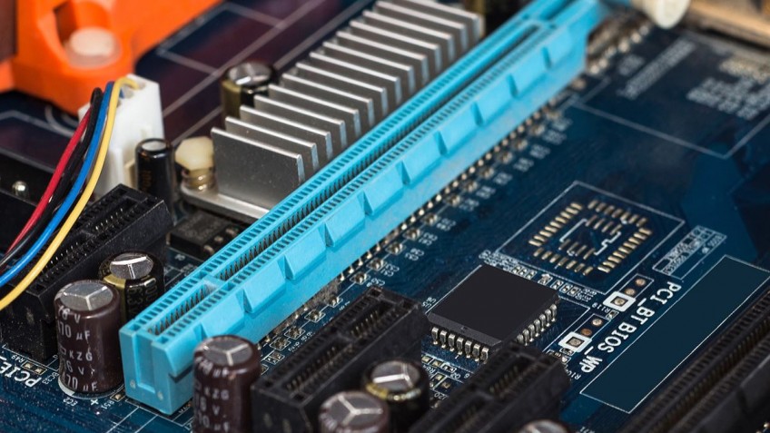
But for the example, it will move into what is called the L0 state, which is the normal operational state where data and packets are sent and received. Once we’ve reached L0, the root complex and endpoint can successfully communicate between each other.
Alternatively, the PCIe link could transition into a number of low power states, or into another link training state called recovery. However, these states are beyond the scope of this video. Please stay tuned for the next video, which will cover the link training and status state machine in more detail.
If all the devices in the PCIe link support PCIe Gen2 or higher data rates, that the link speed may also be increased up to the highest data rate supported. If the new data rate is to be PCIe Gen 3 or higher, the PCIe link will need to go through an additional link optimization process called link equalization.
In link equalization, or Link Eq, the goal is to modify the characteristics of the transmitted data wave form for each part in a way that results in the most stable PCIe link. The PCIe specification defines the ways in which the signal can be modified by providing preset transmitter configurations.
These configurations are aptly called presets. For PCIe Gen 3 and Gen 4, there are 11 presets numbered from 0 to 10 that may be used, each with its own unique signal characteristics. The preset values for each port are negotiated through Link Eq until the ideal preset is chosen.
The downstream port begins this Link Eq process by sending its desired transmitter preset values for each lane to the upstream device. This is referred to as Phase 0 of Link Eq. Shortly after receiving the downstream port’s request, the upstream port increases the data rate of the link to Gen3 and begins transmitting training sequences back to the downstream port using the desired presets.
After the link has been increased to Gen 3 speeds, the Link Eq process continues to optimize the link by sending preset values back and forth to negotiate the preset configuration for each port. The goal of Phase 1 of the Link Eq process is to allow the link to be optimized enough to be able to exchange training sequences and complete the remaining Link Eq phases for fine tuning.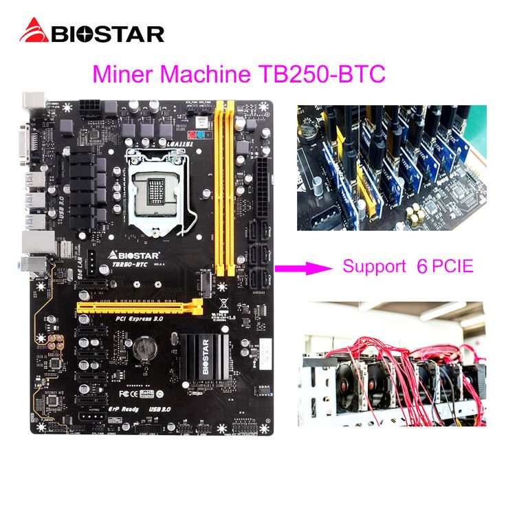
During this phase, identical training sequences will be sent repeatedly to ensure the correct presets are received, despite the possibility of poor link quality.
After Phase 1 has achieved a link with a bit error rate of less than 10 to the negative 4, the link is ready for fine tuning. The negotiation continues with Phase 2, further optimizing the preset values for the upstream port, while Phase 3 performs the same negotiation for the downstream port.
After completing Phase 3 of the Link Eq process, Link Eq is completed, and the Gen3 PCIe link should have a bit error rate less than 10 to the negative 12. In some motherboard designs, particularly those with long channel links, this level of signal quality is not possible. Additional signal conditioning may be required. Fortunately for us, we have a retimer in the link and should have no issues accommodating most any channel length.
The link now moves into a Gen 3 L0 state, and can communicate reliably at Gen 3 speeds.
If you have any questions about PCIe or PCI, please visit our engineer supported forums at e2e.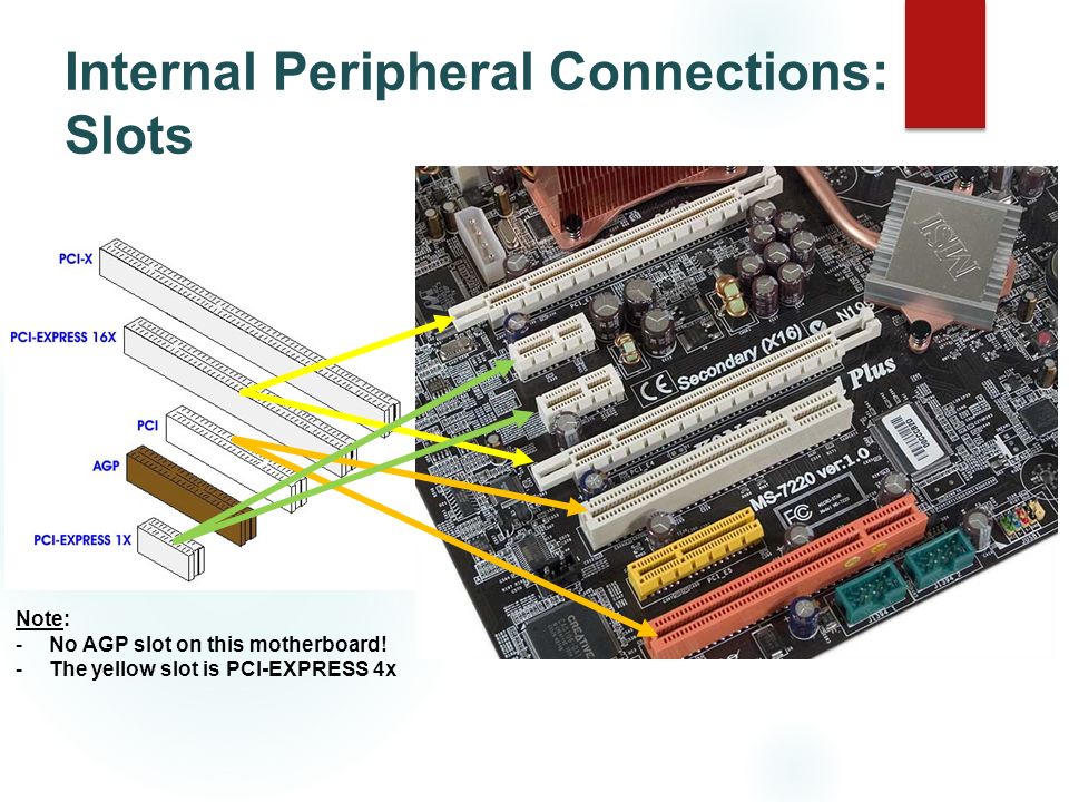 ti.com, and look for us in the Interface section. If you want more information on signal conditioning, please check out our other presentations and our TIPL series. 大家好,欢迎观看 TI 高精度实验室视频。 在本系列中, 我们将讨论外设组件 Internet Connect Express, 通常称为 PCIe。 PCIe 是 2003 年推出的 主板扩展总线标准, 用于在 CPU 及其 外围组件之间实现 高速串行通信。 如今,它已成为 主板扩展总线的 主要标准,并成为 许多其他板载 应用的常用 通信方法。 让我们来探索一下这个 高速接口的发展历史 以及它的工作原理。 PCIe 的前身是 PCI。 在 90 年代, PCI 总线与其他一些 扩展总线技术一起 出现在许多主板上。 主板扩展总线标准 设计用于 CPU 和插入主板 扩展插槽的 设备之间的通信。 最初,所有 扩展总线标准 都使用并行总线,这 意味着数据通过多个通道 发送和接收。 最初,所有 扩展总线标准 都使用并行 总线,这意味着 数据通过多个 通道发送和接收。 在 2003 年 推出时, PCIe 串行 总线标准旨在 取代这些 较旧的并行总线, 以实现更高的数据速率 并简化系统设计。 2003 年,PCI Sig 组织定义了 PCIe 标准。 此后,PCIe 标准随着时间的 推移不断改进, 以适应现代计算机的 最新带宽需求。 今年,即 2021年, 将引入 PCIe 6.0 规范,支持每秒 64 千兆的传输, 或每个链路每秒 64 千兆位的速率。 PCIe 标准的 一个独特功能是 能够将通道数 从 1 个增加到 最多 32 个,以 提高其吞吐量, 这一功能受其并行 总线前身的启发。 16 通道宽的 PCIe 6.0 链路的 数据速率为 每秒 128GB, 按照当今的标准, 这是非常快的。 PCIe 通信 是分层的, 这意味着所有 数据都通过一个 单一的源进行传输, 即,根复合体。 信息从多个 PCIe 端点传递到 根复合体。 让我们详细了解一下 PCIe 如何通过此处 突出显示的典型链路 进行初始化和通信。 我们这里有一个图表, 其中包含 PCIe 链路中 常见的设备。 根复合体是系统 CPU 和内存以及 PCIe 结构其余 部分之间的接口。 根复合体要么 直接集成到 CPU 中, 要么作为一个离散 组件位于 CPU 外部。 中继器是一种 信号调节装置。 有关信号调节器的 更多信息, 请参阅“什么是 信号调节器?”视频。 中继器可分为两类: 重定时器和转接驱动器。 两者都是 常用的 PCIe 组件, 用于保持高速 链路的信号质量。 在我们的示例中,我们将使用 与 PCIe 4.
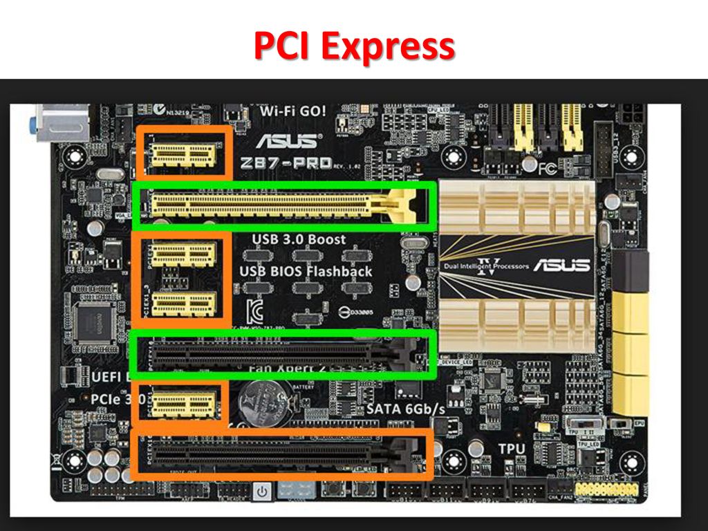 0 兼容的重定时器。 端点是 PCIe 终端 组件的通用术语。 这可能代表 许多不同类型的 PCIe 设备。 在我们的示例中,假设 端点是一个图形处理 单元或 GPU。 在了解 PCIe 链路 是如何建立的, 以及数据是如何通过 PCIe 协议传输的之前, 让我们先来了解一些 常见 PCIe 控制信号的 功能。 PERST 被 称为基础复位。 应将其保持在低位, 直到系统中的所有电源轨 稳定。 该信号从低 到高的转换 通常表示链路 初始化的开始。 WAKE 和 CLKREQ 信号都用于在本 视频范围 之外的低功率 状态之间转换。 有关更多信息, 请参阅即将发布的 培训链接和 状态机视频链接。 REFCLK 是 PCIe 设备开始数据传输的 先决条件。 PCIe 设备使用该 100MHz 参考时钟 信号在链路内 生成高速 PCIe 数据。 PCIe 链路中的 所有设备通电并 提供参考时钟后, PCIe 设备 将在每个通道上 具有接收器检测 电路,该电路将允许 其确定是否有要配对的 链路伙伴。 假设 PCIe Rx 检测 电路看到另一个设备, 则每个通道将开始 以每秒 2.5 千兆位的 速度传输串行数据。 这是原始 PCIe 1.0 规范中 指定的最低 和最基本的 PCIe 数据速率。 PCIe 1.0,也 称为 PCIe 第 1 代, 与任何 PCIe 设备兼容。 因此,每个 PCIe 链路都 将从相同的链路初始化 过程开始。 在此示例中,根 复合体、重定时器 和端点都将以 PCIe 第 1 代的 速度开始传输称为 训练序列的有序数据集, 以建立位和符号锁定。 PCIe 链路初始化 阶段称为轮询阶段。 之后,每个器件 将能够解释 接收到的数据 并做出相应的响应。 这允许 PCIe 连接开始链路 训练过程 并进入配置 阶段。 在配置阶段,将 发生通道到 通道[听不清]过程, 在该过程中,由于 通道长度变化而 导致的数据中的任何 未对准都得到补偿。 PCIe 链路宽度 也在此阶段确定。 在此过程结束时, 每个通道 将与特定的 链路编号以及 该链路内的 通道编号相关联。 如果存在多条 链路,则 PCIe 连接 称为分叉。 然而,在我们的示例中, 我们有一个非分叉 连接,所有通道都 将分配给链路编号 0。 请记住,由于 PCIe 重定时器, 链路分为两部分。 重定时器两侧的链路 分别进行链路初始化。 确定链路和通道号后, PCIe 链路可以 进入多种状态。 例如,它将进入 所谓的 L0 状态,这是 发送和接收 数据和数据包的 正常操作状态。 到达 L0 后, 根复合体和端点 就可以成功地 彼此之间相互通信。 或者,PCIe 链路也可以 转换为许多 低功耗状态, 或者转换为另一种 链路训练状态,称为恢复。 但是,这些状态 超出了本视频的范围。 请继续收看 下一个视频, 将更详细地 介绍链路训练和 状态机。 如果 PCIe 链路 中的所有设备 都支持 PCIe 第 2 代 或更高的数据速率, 则链路速度也 可以提高到支持的 最高数据速率。 如果新数据速率为 PCIe 第 3 代或更高, PCIe 链路将需要 经历一个称为链路 均衡的额外 链路优化过程。 在链路均衡 或 Link Eq 中, 目标是以产生 稳定 PCIe 链路的方式修改 每个部分的传输 数据波形的特性。 PCIe 规范 定义了通过 提供预设发送器 配置来修改 信号的方式。 这些配置被 恰当地称为预设。 对于 PCIe 第 3 代和 第 4 代,可以使用 编号为 0 到 10 的 11 个预设, 每个预设都有其 独特的信号特征。 每个端口的预设值 通过链路均衡协商, 直到选择理想的预设。 下游端口通过 向上游设备发送 每个通道所需的 发送器预设值来 开始该链路均衡过程。 这被称为第 0 阶段链路均衡。 在接收到下游 端口的请求后不久, 上游端口增加到 第 3 代链路数据速率, 并开始使用 所需预设将 训练序列发送 回下游端口。 链路速度增加 到第 3 代速度后, 链路均衡过程 通过来回发送 预设值来协商每个 端口的预设配置, 从而继续 优化链路。 链路均衡过程 第 1 阶段的目标 是允许链路 进行充分优化, 以便能够交换训练序列 并完成剩余的链路 均衡阶段以进行微调。 在这个阶段, 相同的训练序列 将被重复发送, 以确保接收到 正确的预设,尽管 链路质量可能很差。 质量。 在第 1 阶段 实现到 -4 的 误码率小于 10 的链路后, 链路准备好 进行微调。 协商继续进行 到第 2 阶段, 进一步优化上游 端口的预设值, 而第 3 阶段 对下游端口 执行相同的协商。 完成链路均衡 过程的第 3 阶段后, 链路均衡完成, 第 3 代 PCIe 链路的 误比特率 应小于 10 达到 -12。 在某些主板 设计中,尤其是 那些具有长通道 链路的主板,这种信号 质量水平是不可能的。 可能需要 额外的信号调节。 幸运的是,我们在 链路中有一个重定时器, 在适应大多数 通道长度时应该 没有问题。 该链路现在进入 第 3 代 L0 阶段, 并能以第 3 代 速度可靠通信。 如果您对 PCIe 或 PCI 有任何疑问, 请访问我们的工程师 支持论坛 e2e.
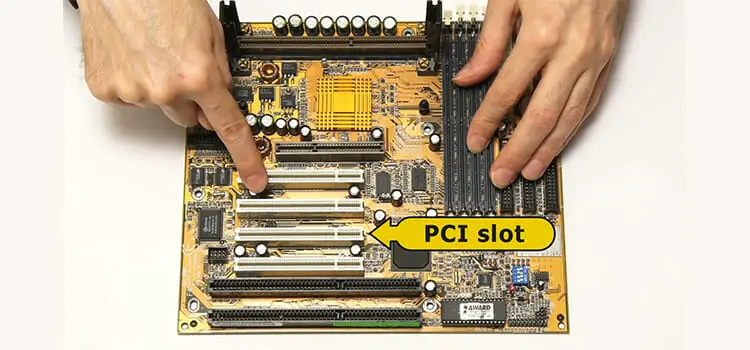 ti.com, 并在界面部分 找到我们的联系信息。 如果您想了解更多 有关信号调节的信息, 请查看我们的 其他演示文稿 和 TIPL 系列。
Next
Description
May 19, 2021
In this video, we discuss the development of the PCIe standard and it’s common applications. It also will give a brief introduction into how a PCIe link is established during link initializing, including the steps involved in link training, and how signal conditioning should be considered in your next PCIe design.
Download webinar slides
Additional information
What is PCIe (PCI Express)?
PCI Express (Peripheral Component Interconnect Express) or as often abbreviated « PCIe » or « PCI-E » is a standard connection type for internal devices in a computer.
Currently, PCI Express refers to modern motherboard expansion slots that accept various PCIe-based expansion cards (sound cards, network cards, etc.).
PCI Express has practically replaced AGP and PCI, which in turn have replaced the old connection type called ISA.
Although computers may have various types of expansion slots, PCI Express is considered a standard internal interface. Many computer motherboards today are made with only PCIe slots.
How does PCI Express work?
Like older standards such as PCI and AGP, PCI Express based devices are physically plugged into a PCI Express slot on the motherboard.
The PCI Express interface provides high bandwidth between devices and the motherboard and other equipment.
There is also an external version of PCI Express, it is called External PCI Express, but often shortened to ePCIe (used more often in mining when you need to connect several video cards to one motherboard).
What are the PCI Express formats?
«PCI Express x1» … «PCI Express 3.0» … «PCI Express x16». What does «x» mean? How do you know what your computer supports? Does a PCI Express x1 card work with a PCI Express x16 slot? If you’re asking the same questions, don’t worry, you’re not alone!
When you buy an expansion card for your computer, such as a new graphics card, it’s often not clear which of the various PCIe technologies is best and which one will work with your PC.
However, as complicated as this may sound, it’s actually quite simple if you understand two important things about PCIe — the first part of the name describes the physical size, the second part of the name describes the version of the technology. More details below.
PCIe sizes: x1, x4, x8, x16
As the subtitle suggests, the number after “
PCIe cards fit any PCIe slot on the motherboard, at least that size. For example, a PCIe x1 card will fit in any PCIe x4, PCIe x8, or PCIe x16 slot. A PCIe x8 card will fit in any PCIe x8 or PCIe x16 slot.
PCIe cards that are larger than the size of the PCIe slot can also fit in the smaller slot, but only if the PCIe slot is open, ie. does not have partitions at the end of the slot.
PCIe versions: 1.0, 2.0, 3.0, 4.0
Any number after PCIe that appears on the product (device) or motherboard indicates the latest supported PCI Express version number.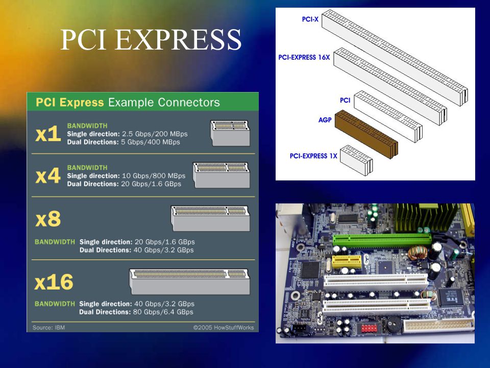
Comparison of versions of PCI Express:
| version | Passing capacity | Passing capacity (PCIe X16) | PCI | GBIT/SA (250 900 MBIT/SA | 32 Gbit/s (4000 MB/s) |
| PCI Express 2.0 | 4 Gbit/S (500 MB/S) | 64 Gbit/S (8000 MB/S) | |||
| PCI Express 3.0 | 7.877 Gbit/S (984.625 MB/S) | 126.032 Gbit/S (15754 MB/S) | |||
| PCI Express 4.0 | 15.752 Gbit/S (1969 MB/S) | 252.032 Gbit/S (31504 MB/S) |
PCI all. Express are both backwards and forwards compatible, which means that no matter what version your PCIe card or your motherboard supports, they should work together.
As you can see from the table, major updates to the PCIe standard each time dramatically increased throughput.
The upgrades have fixed bugs, added features, and improved power management, but the bandwidth increase is the most important change from release to release.
Maximum PCIe Compatibility
For maximum performance (i.e. the highest throughput), select the highest PCIe version your motherboard supports, as well as the largest PCIe size.
For example, a PCIe 3.0 x16 graphics card will only provide maximum performance if the motherboard also supports PCIe 3.0 and has a free PCIe x16 slot. If the motherboard only supports PCIe 2.0, the card will only operate up to the speed supported by PCIe 2.0 i.e. 64 Gb/s in x16 slot.
What will replace PCIe in the future?
Video game developers always strive to create games that are even more realistic, but can only do so if they can transfer large amounts of data, which requires faster interfaces.
PCI Express 5.0, introduced in 2019, supports 31.504 GB/s per lane (3938 MB/s), double that of PCIe 4.0.
The IT world is considering a number of other non-PCIe interface standards, but since these will require major hardware changes, PCIe is likely to remain the leader for a long time to come.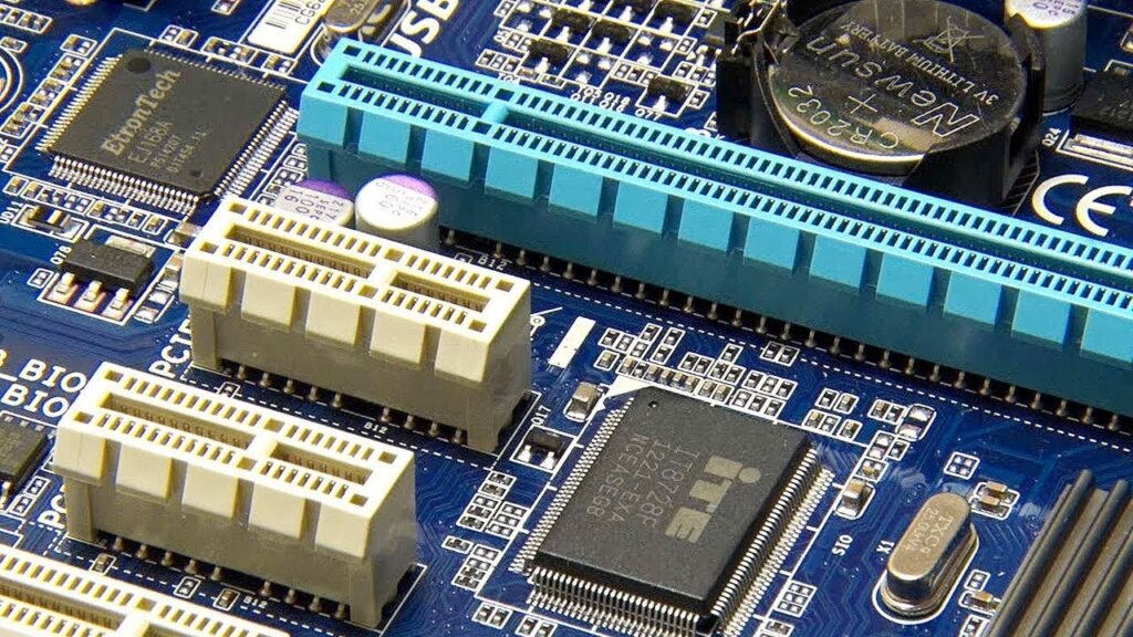
Terminology — PCIe0174 interface based on the PCI software model, but with higher performance and using LVDS and new connectors. Works on high performance serial data protocol. Also known as (3GI0/Arapaho).
Just like the «big brother» PCI, the newer PCIe, with which it has very little in common, is built by the PCI Special Interest Group. PCI Express uses switches to communicate between devices, unlike PCI, which uses a common bus for data transfer. Each new PCI Express bus device is connected directly to the switch via a point-to-point connection.
PCIe appeared in 2002 and was originally aimed only at use as a local bus. At the same time, the user can easily upgrade from PCI to PCIe, without changing the software. PCIe is successfully used instead of the AGP bus (it is also called a special version of AGP), being a successful replacement for the outgoing PCI. In fact, PCIe has successfully replaced all existing buses in PCs (PCI, PCI-X, AGP).
Connectors
- Mini Card,
- ExpressCard,
- AdvancedTCA,
- Mobile PCI Express Module.

The design of the slot prevents the device from working in a slot designed for cards with a lower bandwidth of the PCI Express bus. For example, an x4 card will not fit in a standard x1 slot, even though it could theoretically work in an x4 slot using only one lane. However, some motherboards implement non-standard x1 and x4 slots that do not have an edge baffle, which allows you to install cards longer than the slot itself. This does not provide power and ground to the protruding part of the card.
PCI Express bus supports:
- hot swap cards,
- energy management,
- data integrity control,
- QoS system,
- guaranteed bandwidth.
The PCIe parallel transfer protocol allows the user to scale (1x, 2x, 4x, 8x, 16x and 32x).
The frequency of the PCI Express bus is 2.5 GHz, which provides a bandwidth of 2500 MHz / 10 * 8 = 250 * 8 Mbps = 250 Mbps (due to redundant coding, 10 bits of information are actually transmitted to transfer 8 data bits) for each PCI Express x1 device in one direction.