AMD Radeon HD 7970 3GB Review
Written by
Harry Butler
December 22, 2011 | 08:19
Tags: #28nm #best-graphics-card #directx-11 #radeon #southern-islands #zerocore
Companies: #amd
1 — AMD Radeon HD 7970 3GB Review2 — AMD Radeon HD 7970 3GB — The Card3 — Test Setup4 — AMD Radeon HD 7970 3GB Arma II Performance5 — AMD Radeon HD 7970 3GB Battlefield 3 Performance6 — AMD Radeon HD 7970 3GB Dirt 3 Performance7 — AMD Radeon HD 7970 3GB Skyrim Performance 8 — AMD Radeon HD 7970 3GB Power and Thermals9 — AMD Radeon HD 7970 3GB Overclocking10 — Performance Analysis and Conclusion
Manufacturer: AMD
UK Price (as reviewed): Released 9 January 2012, approx. £440 (inc VAT)
US Price (as reviewed): Released 9 January 2012, $549 (ex tax)
It’s been a quiet year for graphics. With both AMD and Nvidia playing their current generation’s hand by March 2011 with the arrival of the GeForce GTX 590 3GB and the Radeon HD 6990 4GB, the rest of the year has only seen minor or limited-run releases such as the GeForce GTX 560 Ti 448 1.3GB or the Radeon HD 6790 1GB.
However, with Intel’s Ivy Bridge processor rumbling closer, the next round of upgrades beckons, and it’s AMD that’s first out of the traps with the Radeon HD 7970 3GB, the world’s first consumer 28nm GPU. This will be the first of a whole new family of 28nm HD 7000-series GPUs, the rest of which will be released gradually over the first six months of 2012. For now though, the HD 7970 3GB will co-exist with the existing HD 6000-series GPUs, and its £440 price puts it well into the premium graphics bracket.
Ohhhhh, Shiny….
Out with the old, in with the new
Codenamed Tahiti XT, AMD has made some radical changes for its first 28nm GPU. The entire stream processor layout has been altered, with the 24 SIMD Engines of Caymen XT replaced by 32 individual compute units (CUs), which AMD has chosen to dub Graphics Core Nexts (GCNs). Poor English aside, each CU (no, we’re not going to call them GCNs) contains four SIMD Engines, with each of these equipped with 16 stream processors and its own vector units and 64KB vector register. This means each CU therefore includes 64 stream processors and the GPU as a whole wields 2,048 stream processors; 512 more than the previous top-end Caymen XT.
Out of the box the GPU runs at 925MHz — a 5 per cent increase over the HD 6970 2GB’s 880MHz frequency. Each CU is also equipped with four texture units (the same as for each SIMD Engine in Caymen XT), resulting in a total of 128 texture units for the whole GPU.
The Tahiti XT architecture is a big change for AMD
This increasingly parallel design (there are effectively now 128 SIMD Engines with 16 stream processors each, as opposed to 24 SIMD Engines of 64 stream processors each in Caymen XT), combined with a pair of front end units, should make Tahiti XT an effective multi-tasker, particularly when it comes to GPGPU, a field in which AMD’s GPUs have typically languished behind those of Nvidia.
The new CU layout also sees the abandonment of the VLIW (Very Long Instruction Word) design philosophy that has typified AMD GPUs as far back as the Radeon HD 2900 XT. This is a significant change for AMD, and brings it into line with Nvidia’s modular Fermi-based GPUs. AMD claims the move away from VLIW, along with the new CU layout, significantly simplifies the GPU’s render process, making the GPU’s performance more predictable and in need of less optimisation.
As we’ve already said, AMD has once again used a dual front-end engine design for Tahiti XT, although it’s notably different from that of its predecessor. Each front end unit’s geometry assembler, vertex assembler and ninth generation tessellator have been merged into a geometry engine, with the rasteriser in a separate unit. AMD claims this new layout has significantly improved the GPU’s tessellation performance, with up to four times the throughput of the HD 6900 design. Also new to the pair of front end engines is an asynchronous compute engine (ACE) each, further underlining AMD’s focus on GPGPU performance by allowing compute and graphics operations to enter the GPU simultaneously.
The GPU’s memory has also been given a boost. Six 64-bit dual channel memory controllers each connect to two 256MB GDDR5 memory modules, making for a staggering 3GB of video memory in total, which is connected via a fat 384-bit bus. Combined with a memory frequency of 1,375MHz (5.5GHz effective), the HD 7970 3GB boasts a mighty 264GB/sec of memory bandwidth, making it well suited to ultra-high resolutions such as those of Eyefinity setups.
Rounding out the GPU’s vital statistics are eight render back-end units, each with four ROPs for a combined total of 32 ROPs, which has been the standard number for AMD’s high end GPUs for the last few generations. All in all AMD has somehow managed to cram 4.3 billion transistors into the 365mm² GPU die; an increase of 65 per cent compared with the previous high-end Cayman XT GPU, and in a 6 per cent smaller die.
1 — AMD Radeon HD 7970 3GB Review2 — AMD Radeon HD 7970 3GB — The Card3 — Test Setup4 — AMD Radeon HD 7970 3GB Arma II Performance5 — AMD Radeon HD 7970 3GB Battlefield 3 Performance6 — AMD Radeon HD 7970 3GB Dirt 3 Performance7 — AMD Radeon HD 7970 3GB Skyrim Performance 8 — AMD Radeon HD 7970 3GB Power and Thermals9 — AMD Radeon HD 7970 3GB Overclocking10 — Performance Analysis and Conclusion
AMD Radeon HD 7970 GHz Edition review
Skip to main content
When you purchase through links on our site, we may earn an affiliate commission. Here’s how it works.
Recommended
Back to the top of the performance tree
TechRadar Verdict
A great refresh of the HD 7970, but doesn’t warrant the massive price premium over the original.
TODAY’S BEST DEALS
Pros
- +
Lightning fast performance
- +
Great compute performance
- +
Top GPU on the block
Cons
- —
Incredibly expensive
- —
And not great value with it
Why you can trust TechRadar
Our expert reviewers spend hours testing and comparing products and services so you can choose the best for you. Find out more about how we test.
AMD’s Radeon HD 7970 reached its six-month birthday on June 22nd 2012, and to celebrate AMD has released a card that’s just, well, better: the AMD Radeon HD 7970 GHz Edition.
Since it released the original Radeon HD 7970, in December last, the top single-GPU graphics card crown has slipped from its once mighty, and once mightily expensive, head. Nvidia waited, holding its breath until March, when it released its top consumer spin of the new Kepler architecture, the Nvidia GeForce GTX 680.
That came in slightly undercutting the Radeon card and just about pipping it to the benchmark crown in most of our tests. Not just that but the Nvidia GTX 680 managed it with a far smaller and more efficient GPU.
To most of us that came as something of a surprise.
AMD traditionally had the reputation of releasing the more efficient GPUs of a generation with Nvidia usually the ones employing a brute force approach with a big, hot and powerful chip at the heart of its latest architecture.
That switch wasn’t the only one of this latest generation either. AMD’s Graphics Core Next (GCN) architecture — which makes up the Southern Island series of HD 7000 graphics cards — was conceived with a view to creating a much more compute focused card. Previous to this architecture AMD had focused on creating pure gaming cards with only a faint nod towards GPGPU processing.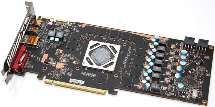
Nvidia, on the other hand, chose performance per Watt for its consumer cards and sacrificed the GPGPU computing power that had been central to the Fermi architecture. This cut-down GPU though was still a great gaming chip, as the Nvidia GeForce GTX 680 showed, leaving the Tesla team, with the GK110 K20, to the pro-graphics compute shizzle.
Still, it managed to best AMD’s top card in most gaming benchmarks leaving it with the runners up prize.
Until now.
Vital stats
GPU
— Tahiti XT
Process
— 28nm
Clockspeed
— 1,050MHz
Memory capacity
— 3GB GDDR5
Memory bus
— 384-bit
The AMD Radeon HD 7970 GHz Edition is the Texan company’s counter-offer to gamers in light of the slight lead Nvidia managed with the GTX 680. And to be fair, it’s come up with quite an interesting proposal.
The salient point here though is that AMD has reclaimed the outright single-GPU performance crown of this generation. Obviously that’s discounting the twin-GPU toting Nvidia GTX 690, which has almost cheated its way to the top of the graphics card pile.
Though AMD had planned an assault on even that position, promising us the card once code-named as New Zealand. You know, the place that has two Southern Islands making up the country.
Get it?
Still, for whatever reason that card is off the table now with AMD focusing its efforts on bolstering the Tahiti GPU-sporting HD 7970 and making it the top single-GPU card around.
So, how has it managed this feat?
Well, the simple answer is overclocking. We told you it was simple.
But this isn’t quite the traditional card speed bump, or manufacturer-supported factory overclocked card you might normally expect. Nothing has actually changed regarding the GPU itself.
AMD is still taking them from the same wafers, with the same designs, but it has taken the six months of learning that went into the subsequent Pitcairn and Cape Verde GPUs and applied it to the flagship chip. Basically the GPU manufacturing process has matured and so has the technology and, most importantly, the software.
This has enabled AMD to get more top-end Tahiti cores out of the wafers and so is offering the AMD Radeon HD 7970 GHz Edition with a clockspeed of, you guessed it, 1GHz.
Though that’s not strictly true.
In reality the clockspeed you’re realistically going to get when gaming is actually 1.05GHz.
That extra 50MHz coming from something AMD is calling PowerTune with Boost. The idea being similar in concept to Nvidia’s GPU Boost, with some new hardware on the PCB monitoring the voltage and offering extra power, up to that 1.05GHz mark, when the thermal headroom allows.
In our testing that was all of the time, even with the standard reference cooler design. Our reference AMD Radeon HD 7970 GHz Edition sat at a stable 1.05GHz for the entire time the GPU was pushed to 100% load.
The only other real addition of note to the card is the 3GB of GDDR5 graphics memory has been given a bit of a speed boost too. The stock card has a 1,375MHz speed for its memory while the AMD Radeon HD 7970 GHz Edition comes with the VRAM running at a healthy 1,500MHz.
That’s not all though as the type of memory used has been changed too. This time it is using the faster 6Gbps VRAM over the 5.5Gbps chips it had been rocking, the same speedy memory the Nvidia GTX 680 is sporting then.
Thanks to AMD’s faster 384-bit memory bus though the Radeon HD 7970 GHz Edition has a massive 288GB/s memory bandwidth compared with the 192GB/s of the top single-GPU Nvidia card. That means at the higher end of the resolution spectrum the AMD card now seriously has the edge.
AMD Radeon HD 7970 GHz Edition: Price Comparison
No price information
Check Amazon
powered by
- 1
Current page:
Introduction and Architecture
Next Page Benchmarks
TechRadar is part of Future US Inc, an international media group and leading digital publisher. Visit our corporate site .
©
Future US, Inc. Full 7th Floor, 130 West 42nd Street,
New York,
NY 10036.
AMD Radeon HD 7970 3 GB GDDR5 GECID.com review and test. Page 1
::>Video cards
>2012
> AMD Radeon HD 7970
01/22/2012
Page 1
Page 2
One page
Presentation of the new generation of AMD GPUs has certainly become one of the most significant events of the last quarter of 2011 in the IT industry. In an arms race with NVIDIA, the Sunnyvale semiconductor giant made a very important strategic move by being the first to introduce the next generation of GPUs based on 28nm chips.
Thus, AMD once again gained some advantage over its main competitor in the discrete graphics market. By the time the first representatives of the 600th line of NVIDIA GeForce GPUs appear on sale, solutions based on the Radeon HD 7970 will already be on the market for at least a couple of months, which will increase their sales level, especially among advanced gamers and enthusiasts who want to get hi-end new products as soon as possible.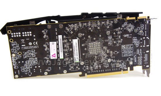 Radeon HD 79 demo70, held in Moscow on December 13, made a very good impression on us, but only a month later we finally managed to get a sample of the AMD Radeon HD 7970 video card to our test lab. However, before proceeding directly to studying the features of the AMD Radeon HD 7970 graphics accelerator itself, it is worth talking about the architectural features of the Tahiti XT graphics core, which underlies it.
Graphics Core Next 9 Architectural Features0012
Recall that starting from the Radeon HD 2000 line, ATI (and later AMD) engineers used the VLIW (very long instruction word) architecture to develop Radeon graphics processors. Of course, since the introduction of the R600 chip to the Northern Island family of graphics adapters, the performance of solutions has increased several times, but there have been no fundamentally new changes during this time.
Nevertheless, the quality of graphics in PC games is constantly improving, and developers are finding new ways to increase the realism of the image on the monitor screen. Of course, the requirements for the speed and memory of video cards are constantly growing, but the nature of the tasks that they face is gradually changing. So, for example, recently discrete graphics adapters are increasingly being used in “non-graphical” applications and often the performance of a certain task by a video card requires less time and resources. This is one of the highest priority development trends for graphics chip manufacturers, and AMD and NVIDIA are well aware of this. Note that the developers from the «green camp» realized the need to create a fundamentally new unified architecture and a general-purpose graphics chip (GPGPU or General Purpose GPU) much earlier. As a result, NVIDIA CUDA technology is now supported by a large number of programs, including professional solutions. However, this technology has received significant distribution relatively recently, so AMD still has every chance to compete in this market segment.
So, the basis of the new Tahiti XT chip based on the Graphics Core Next architecture is super-scalar processors called Compute Units, which include 64 ALUs each. It is important to note that they consist of vector and scalar blocks, and also have a built-in scheduler and 16 kilobytes of L1 cache. The applied scheme of their structure allows to obtain higher performance in comparison with the VLIW-architecture, as well as high efficiency, both for solving graphic tasks and general-purpose tasks.
In total, the Tahiti XT chip includes 32 Compute Units (2048 stream processors), which are divided into groups of 4 pieces. Each such group has at its disposal 32 KB of cache memory for storing data and 16 KB for instructions. In addition, as we have already noted, each CU is equipped with its own 16 KB cache. The total amount of cache in the first level (L1) is 512 KB, and the second — 768 KB, which is twice as much as the previous flagship of the Radeon HD line.
The memory bus width was increased to 384 bits, but the number of ROPs did not increase proportionally to 48, but remained the same — 32. At the same time, the principle of their interaction with the rest of the GPU, according to AMD engineers, was significantly redesigned . Note that the new Tahiti XT chip includes 4.31 billion transistors in an area of 365 mm².
Particular attention in the new architecture, according to AMD representatives, was given to the tessellation block. Since the days of the Radeon HD 5000 line, in tasks with the active use of tessellation, solutions from NVIDIA have looked much more preferable, however, with the introduction of the tessellation unit of the tenth version in the Radeon HD 7000 line, the situation may change significantly.
Based on graphics from AMD’s official presentation, compared to the previous flagship, Radeon HD 7970’s tessellation processing performance has increased by up to 140% in certain applications.
An important innovation in the new Graphics Core Next architecture is the separate Video Codec Engine block. When software appears on the market that allows you to take full advantage of its capabilities, users will be able to use the processing power of video accelerators not only for decoding, but also for encoding video content.
A lot of attention in the new architecture has traditionally been paid to energy consumption. AMD Power Tune technology is designed to dynamically monitor the load on the GPU and, if the maximum TDP level is exceeded (for example, in FurMark, OCCT stress tests), it automatically reduces the GPU clock speed and its voltage. Thus, the manufacturer does not artificially reduce the performance of the video card, looking only at synthetic tests, which practically do not run in real operation.
Another nice feature of the Graphics Core Next is the ZeroCore feature. Now in idle mode, after the monitor screen automatically turns off, the video card can automatically switch to economy mode, even turning off the cooling fan. The power consumption of the graphics adapter in this mode does not exceed 4 watts, according to AMD engineers.
In CrossFireX mode, when switching to 2D mode, all adapters except one will similarly «sleep» and turn off the CO fans.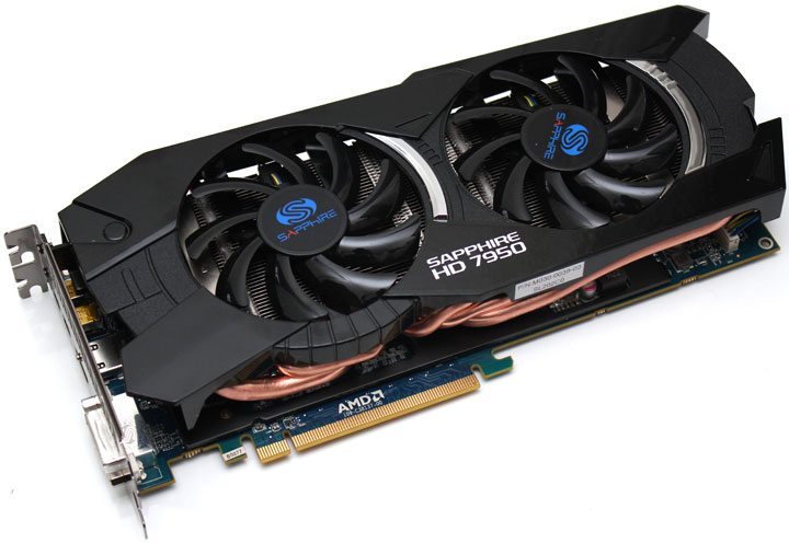
A lot of attention in the new architecture was also paid to Eyefinity technology, which, we recall, allows you to connect multiple displays to one video card in different modes at the same time. With the transition to Graphics Core Next, Eyefinity technology has been updated to the second version and now allows you not only to connect up to 6 monitors to one video card (using active adapters, purchased separately), but also to activate 3D mode when connecting multiple displays. Here again, AMD sets a new standard in the industry, because the similar NVIDIA 3D Vision Surround mode requires at least 2 graphics cards in SLI mode.
In addition, AMD Radeon HD 7970 is announced to support monitors and LCD panels of ultra-high resolution (7680 × 4320 pixels), which at the moment is already a good start for the future. Also, it should be noted that the video cards of the Southern Islands family support the PCI Express 3.0 interface. There is still little practical benefit from this innovation, however, the fact that new standards are being introduced is certainly pleasant. Note that the AMD Radeon HD 7970 is the first video card on the market to support PCI Express 3.0. At the end of the story about the architecture, here is a summary table in which we compared the specifications of the new flagship of the Radeon HD line with its predecessors and current competitors:
|
AMD Radeon HD 7970 |
AMD Radeon HD 6970 |
AMD Radeon HD 5870 |
NVIDIA GeForce GTX 580 |
|
|
Codename |
Tahiti XT |
Cayman XT |
Cypress |
GF 110 |
|
Number of stream processors |
2048 |
1536 |
1600 |
512 |
|
Texture blocks |
128 |
96 |
80 |
64 |
|
ROPs |
32 |
32 |
32 |
48 |
|
GPU frequency, MHz |
925 |
880 |
850 |
772 |
|
Shader frequency, MHz |
925 |
880 |
850 |
1544 |
|
Video memory frequency, MHz |
1375 |
1375 |
1200 |
1002 |
|
GDDR5 memory, MB |
3072 |
2048 |
1024 |
1536 |
|
Video memory interface, bit |
384 |
256 |
256 |
384 |
|
Power connectors |
1 x 6-pin, 1 x 8-pin |
1 x 6-pin, 1 x 8-pin |
1 x 6-pin, 1 x 8-pin |
1 x 6-pin, 1 x 8-pin |
|
Recommended power supply unit W |
500 |
550 |
500 |
600 |
This list of innovations in the Graphics Core Next architecture looks really interesting and promising. Well, we are moving on to practical testing in order to practically study all the features of AMD’s advanced technologies on the example of the «reference» design Radeon HD 7970 video card.
|
Model |
AMD Radeon HD 7970 |
|
|
Graphics core |
AMD Tahiti XT |
|
|
Number of stream processors |
2048 |
|
|
Supported APIs |
DirectX 11.1 (Shader Model 5.0, DirectCompute 11.1), OpenCL 1.2 and OpenGL 4.2 |
|
|
Graphics core frequency, MHz |
925 |
|
|
Memory frequency (effective), MHz |
1375 (5500) |
|
|
Memory size, MB |
3072 |
|
|
Memory type |
GDDR5 |
|
|
Memory bus width, bits |
384 |
1x Single-Link DVI |
|
Support for HDCP and HD video decoding |
Yes |
|
|
Minimum power supply requirement, W |
500 |
|
|
Dimensions, mm |
285 x 111 |
|
|
Drivers |
Fresh drivers can be downloaded: |
|
|
Manufacturer website |
http://www.amd.com/ |
 4
4 It’s worth noting that our test lab did not include a retail version of the Radeon HD 7970, and not even the final revision of this video card. Today we are dealing with an engineering sample that probably has a number of minor differences from those graphics cards based on the Radeon HD 7970, which have already appeared in Ukrainian retail chains. Nevertheless, its main characteristics completely coincide with those declared for the AMD Radeon HD 7970, therefore, the performance level should be similar. Until the time when AMD partners present their versions of the Radeon HD 7970 based on a unique design, all video accelerators based on the Radeon HD 7970 will differ only in a sticker on the cooling system casing, delivery kit, warranty service conditions and, of course, cost.
The appearance of the video card is very similar to the design of the previous flagships of the Radeon line, however, the differences between them are clearly visible, and the Radeon HD 7970 has its own «face». In our opinion, the smoothed edges of the casing of the cooling system and the use of glossy plastic look more attractive in comparison with the strict and somewhat «brick» look of the Radeon HD 6970/6950. The length of the video accelerator is 285 mm, which is typical for hi-end solutions. In most modern gaming cases in the Middle- and Full-Tower format, its location will not cause problems.
The following interfaces are provided for displaying an image on the AMD Radeon HD 7970 video card:
Note that the developer refused the second DVI connector, motivating this by the desire to increase the efficiency of the turbine-type cooling system. It is likely that retail versions of the Radeon HD 7970 will be equipped with additional adapters and the end user should not have any problems connecting a monitor, plasma panel or projector to the video card. Recall that thanks to Eyefinity 2.0 technology to graphics accelerators on AMD Radeon HD 7970, you can connect up to 6 monitors with two additional DisplayPort hubs (sold separately). An HDMI 1.4a port with frame packing support delivers a 3D image at 60Hz to each eye.
The printed circuit board of the AMD Radeon HD 7970 video card that came to our laboratory is made on a red textolite, however, cards on a later revision of the black PCB are supplied to retail channels. Of course, it is worth noting the use of high-quality element base: field-effect transistors in a DirectFET metal case, chokes with ferrite cores and solid-state capacitors.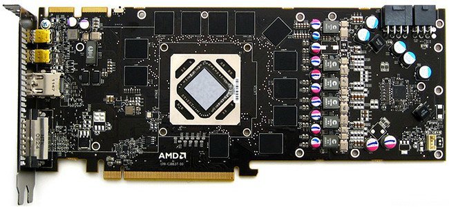 For Radeon HD 79 level solution70 high-quality element base will not only ensure long and stable operation in normal mode, but also allow you to achieve better results during overclocking.
The power stabilization module is made according to a 6 + 1-phase scheme, and the CHiL CHL8228G chip is used as a PWM controller.
To power the video card, in addition to the PCI-E connector, one 6-pin and one 8-pin power connectors are used, which are located on the side at the end of the board.
Two CrossFireX bridge connectors allow multiple AMD GPU-based graphics cards to be connected together to calculate visual effects. Next to them is a small BIOS switch, which first appeared in the Radeon HD 6900 line. Here we found only the mounting cross of the cooling system and a few microcircuits of the VRM module. In addition, on the engineering sample that got to us in the test lab, there were several small switches and connectors for an incomprehensible purpose on the back of the printed circuit board. In the final version, obviously, there is nothing like that.
This is what the Tahiti XT graphics chip looks like, made according to the standards of the 28 nm process, which is the central part of the video card in question. As we already mentioned, it includes 2048 unified processors and 32 ROPs, and data exchange between the graphics core and memory is carried out via a 384-bit bus.
GDDR5 video memory with a total volume of 3 GB is assembled using twelve 256 MB chips manufactured by Hynix. The chips are marked H5GQ2h34MFR T2C and, according to the documentation, can operate at an effective frequency of up to 6 GHz. Considering that the memory in the tested video card initially operates at a frequency of 5500 MHz, it makes sense to try to speed it up a bit during the manual overclocking process.
The cooling system of AMD Radeon HD 7970 «reference» design includes a turbine and a rather massive aluminum radiator at the base of which there is an evaporation chamber, which contributes to an even distribution of heat over the entire heat exchanger area.
For effective air intake, there are special holes in the back of the plastic casing that covers the entire front of the printed circuit board.
The graphics chip is in direct contact with the main heatsink, while the memory chips and power transistors are in contact through a special thermal interface with a metal base plate on which the heatsink and turbine are mounted. On the whole, since the time of the Radeon HD 6970, the standard cooler has not undergone significant changes, and in order to test its effectiveness in practice, we conducted our standard set of tests. Traditionally, tests were carried out in two cooler operating modes: automatic control and maximum turbine speed.
In automatic mode, at maximum load, the temperature of the graphics core did not exceed 74 degrees, which is a good result for an adapter of this level. At the same time, the fan worked at 50% of its power, producing an average noise level that was noticeable against the general background of the system, but not annoying.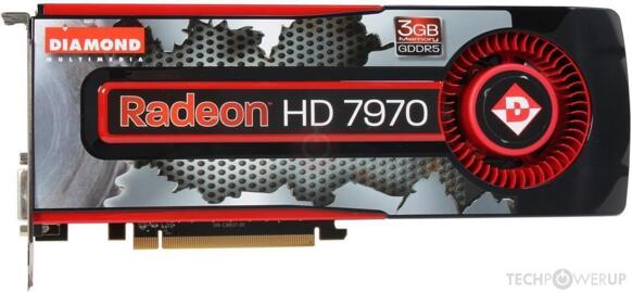
After we set the fan speed to maximum and tested again, we recorded a decrease in the maximum temperature of the GPU by 12 degrees, and the noise level emitted by the cooler, we would describe as very high.
When there is no load, the graphics core and memory frequencies are automatically lowered, resulting in lower power consumption and heat dissipation. The cooler in this mode works really quietly, and the temperature of the graphics core does not exceed 36 degrees.
Overall, the evaporative chamber cooling system used for the AMD Radeon HD 7970, , showed good cooling performance at an average noise level. Against the background of other components of a modern system unit, the noise from the operation of a video card under a typical load stands out insignificantly.
Test & Review: AMD Radeon HD 7970
AMD has decided to start a new battle for dominance in the GPU market. But today, both manufacturers, AMD and Nvidia, have to face new challenges and work in new conditions.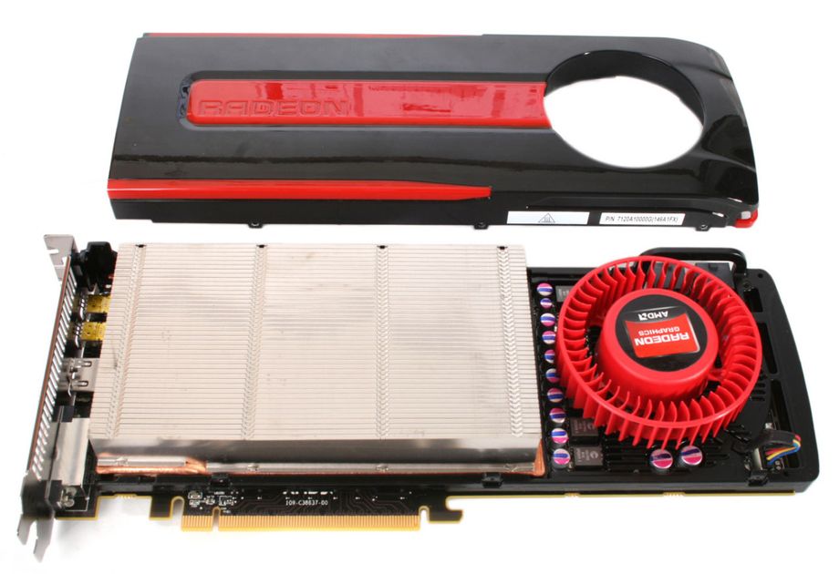 In particular, AMD has to switch to a new 28 nm production technology, and a completely new GPU architecture, as it turned out. NVIDIA also plans to move to 28 nm, but only in a few months, and with a new architecture. But AMD was the first, and in our article we will talk about the new generation of GPUs in the form of AMD Radeon HD 7970.
» Photostrecke
AMD believes that PC gaming is in for a boom, and in the short term — especially given that consoles are updated for quite a long time. And since modern graphics engines benefit from the capabilities of advanced graphics cards, this development will only intensify. The PC games market was worth $15 billion last year and is expected to grow to $20 billion by 2013. And don’t forget that gamers today prefer to play at ever higher resolutions. 1080p resolution has already become the de facto standard, which is supported by rapidly becoming cheaper displays with a large diagonal. In addition, AMD is focusing on higher GPU efficiency and GPU computing capabilities. The latter area is very important for AMD today as the company wants to work around the limitations found in Cayman architecture GPUs.
AMD has only introduced the Radeon HD 7970 so far, as you can see on the slide, but new cards should be coming to the Radeon HD 7900 line soon.
| NVIDIA GeForce GTX 570 |
NVIDIA GeForce GTX 580 |
AMD Radeon HD 6950 | AMD Radeon HD 6970 | AMD Radeon HD 7970 | |
| GPU | GF110 | GF110 | Cayman PRO | Cayman XT | Tahiti XT |
| Process | 40 nm | 40 nm | 40 nm | 40 nm | 28 nm |
| Number of transistors | 3 billion | 3 billion | 2. 6 billion 6 billion |
2.6 billion | 4.3 billion |
| Crystal area | 530 mm² | 530 mm² | 389 mm² | 389 mm² | 365 mm² |
| GPU clock speed | 732 MHz | 772 MHz | 800 MHz | 880 MHz | 925 MHz |
| Memory clock | 950 MHz | 1000 MHz | 1250 MHz | 1375 MHz | 1375 MHz |
| Memory type | GDDR5 | GDDR5 | GDDR5 | GDDR5 | GDDR5 |
| Memory capacity | 1280 MB | 1536 MB | 2048 MB | 2048 MB | 3072 MB |
| Memory bus width | 320 bit | 384 bit | 256 bit | 256 bit | 384 bit |
| Memory bandwidth | 152 GB/s | 192 GB/s | 160 GB/s | 176 GB/s | 264 GB/s |
| Shader model | 5.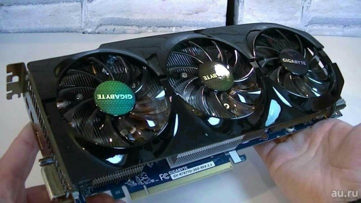 0 0 |
5.0 | 5.0 | 5.0 | 5.0 |
| DirectX | 11 | 11 | 11 | 11 | 11.1 |
| Number of stream processors | 480 (1D) | 512 (1D) | 1408 (352 4D) | 1536 (384 4D) | 2048 (1D) |
| Stream processor clock speed | 1464 MHz | 1544 MHz | 800 MHz | 880 MHz | 925 MHz |
| Number of texture units | 60 | 64 | 88 | 96 | 128 |
| Number ROP | 40 | 48 | 32 | 32 | 32 |
| Maximum power consumption | 219 W | 244 W | 200 W | 250 W | 250W |
| Minimum power consumption | — | 30-32W | 20W | 20W | 2. 6 W 6 W |
| CrossFire/SLI | SLI | SLI | CrossFireX | CrossFireX | CrossFireX |
Radeon HD 79 video card70 is based on the «Tahiti XT» GPU, which is manufactured using a 28nm process. In total, the GPU has 4.3 billion transistors. By comparison, Intel’s Sandy Bridge-E processors (excluding quad-core models) have 2.27 billion transistors. And the predecessor from the Cayman Radeon HD 6900 family worked with 2.6 billion transistors. The crystal area is 365 mm². As you can see, the area is slightly less than 389 mm² for the «Cayman» GPUs, which are manufactured using the 40-nm process technology. NVIDIA’s GF110 GPU contains 3 billion transistors in an area of 530 mm². Most of the GPU transistor budget was spent on 2048 stream processors. GPUs and stream processors run at clock speed 925 MHz. AMD decided to keep the same memory as the Radeon HD 6970, i. e. GDDR5 at 1375 MHz. But the memory interface has been expanded from 256 bits to 384 bits, increasing the memory bandwidth to 264 GB/s. In addition, the capacity has increased from 2048 MB to 3072 MB. The Radeon HD 7970 has 128 texture units and 32 raster operations pipelines (ROPs) — we get an increase in texture units compared to the Radeon HD 6970, but the number of ROPs remains the same. AMD has indicated the maximum power consumption for the Radeon HD 7970 at 250W, which is also the limit for PowerTune. Typical graphics card power consumption is 210W. Let’s recall that the Radeon HD 6970 had a maximum power consumption of 250 watts, and a typical one under load — 190 watts. Thanks to ZeroCore Power technology (more on that below), power consumption in idle mode does not exceed three watts.
GPU-Z 0.5.7, as you can see in the screenshot, does not correctly display all AMD Radeon HD 7970 data. On our test system, the Socket 1366 interface was specified as PCI Express 3.