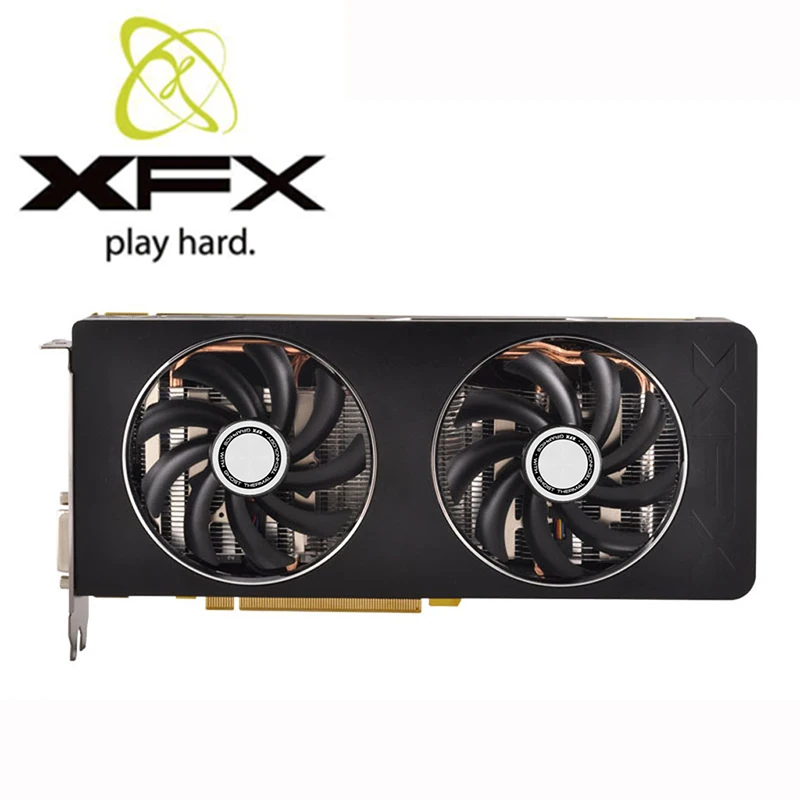
Radeon R9 370 [in 2 benchmarks]
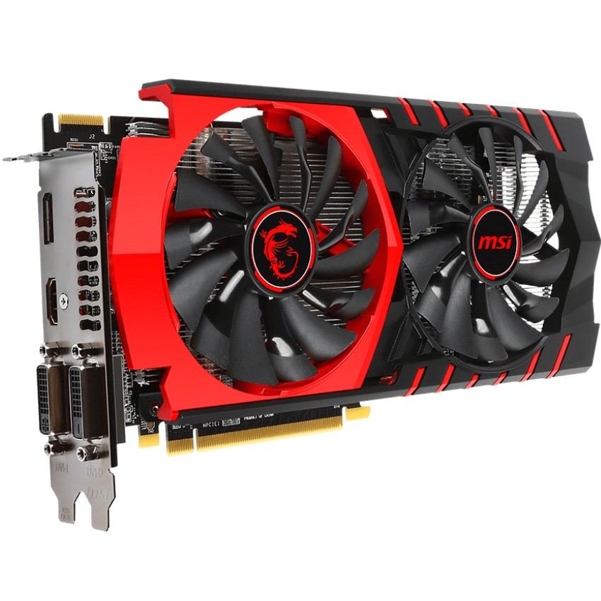
Radeon R9 370
Buy
- Interface PCIe 3.0 x16
- Core clock speed 925 MHz
- Max video memory 4096
- Memory type GDDR5
- Memory clock speed 5600 MHz
- Maximum resolution
Summary
AMD started Radeon R9 370 sales 5 May 2015. This is GCN 1.0 architecture desktop card based on 28 nm manufacturing process and primarily aimed at gamers. 4 GB of GDDR5 memory clocked at 5.6 GHz are supplied, and together with 256 Bit memory interface this creates a bandwidth of 179.2 GB/s.
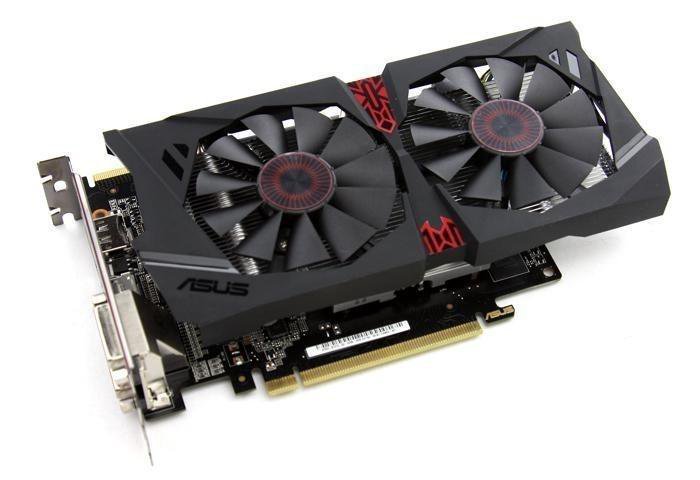
Compatibility-wise, this is dual-slot card attached via PCIe 3.0 x16 interface. Its manufacturer default version has a length of 221 mm. 1x 6-pin power connector is required, and power consumption is at 110 Watt.
It provides poor gaming and benchmark performance at
16. 08%
of a leader’s which is NVIDIA GeForce RTX 3090 Ti.
Radeon R9
370
vs
GeForce RTX
3090 Ti
General info
Of Radeon R9 370’s architecture, market segment and release date.
| Place in performance rating | 286 | |
| Value for money | 4.04 | |
| Architecture | GCN 1.0 (2012−2020) | |
| GPU code name | Trinidad | |
| Market segment | Desktop | |
| Release date | 5 May 2015 (7 years ago) | |
| Current price | $337 | of 49999 (A100 SXM4) |
Value for money
To get the index we compare the characteristics of video cards and their relative prices.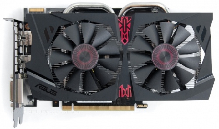
- 0
- 50
- 100
Technical specs
Radeon R9 370’s general performance parameters such as number of shaders, GPU base clock, manufacturing process, texturing and calculation speed. These parameters indirectly speak of Radeon R9 370’s performance, but for precise assessment you have to consider its benchmark and gaming test results.
| Pipelines / CUDA cores | 1280 | of 18432 (AD102) |
| Core clock speed | 925 MHz | of 2610 (Radeon RX 6500 XT) |
| Boost clock speed | 975 MHz | of 2903 (Radeon Pro W6600) |
| Number of transistors | 2,800 million | of 14400 (GeForce GTX 1080 SLI Mobile) |
| Manufacturing process technology | 28 nm | of 4 (h200 PCIe) |
| Thermal design power (TDP) | 110 Watt | of 900 (Tesla S2050) |
| Texture fill rate | 78.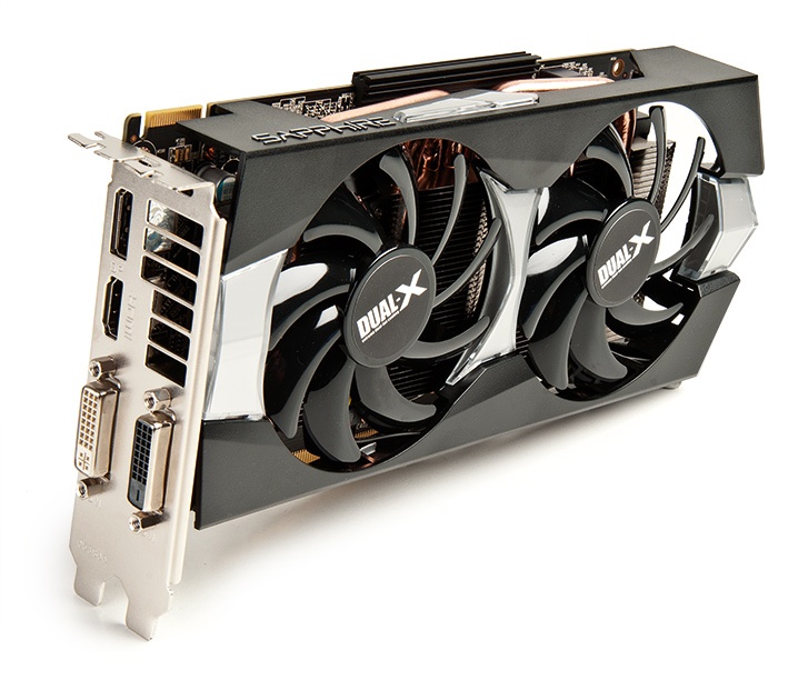 00 00 |
of 939.8 (h200 SXM5) |
| Floating-point performance | 2,496 gflops | of 16384 (Radeon Pro Duo) |
Compatibility, dimensions and requirements
Information on Radeon R9 370’s compatibility with other computer components. Useful when choosing a future computer configuration or upgrading an existing one. For desktop video cards it’s interface and bus (motherboard compatibility), additional power connectors (power supply compatibility).
| Interface | PCIe 3.0 x16 | |
| Length | 221 mm | |
| Width | 2-slot | |
| Supplementary power connectors | 1x 6-pin |
Memory
Parameters of memory installed on Radeon R9 370: its type, size, bus, clock and resulting bandwidth. Note that GPUs integrated into processors don’t have dedicated memory and use a shared part of system RAM.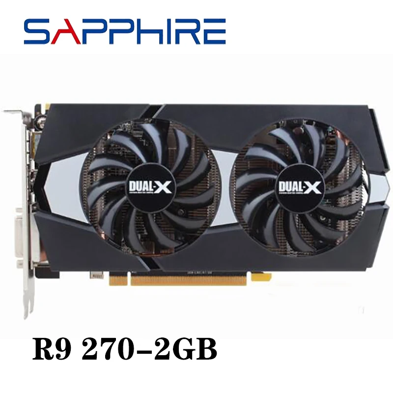
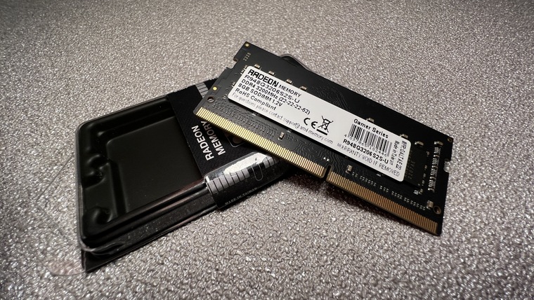
| Memory type | GDDR5 | |
| Maximum RAM amount | 4 GB | of 128 (Radeon Instinct MI250X) |
| Memory bus width | 256 Bit | of 8192 (Radeon Instinct MI250X) |
| Memory clock speed | 5600 MHz | of 21000 (GeForce RTX 3090 Ti) |
| Memory bandwidth | 179.2 GB/s | of 14400 (Radeon R7 M260) |
Video outputs and ports
Types and number of video connectors present on Radeon R9 370. As a rule, this section is relevant only for desktop reference video cards, since for notebook ones the availability of certain video outputs depends on the laptop model.
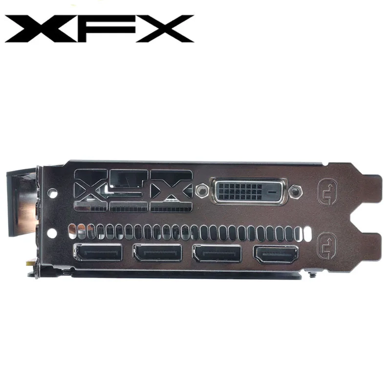
| Display Connectors | 2x DVI, 1x HDMI, 1x DisplayPort | |
| HDMI | + |
API support
APIs supported by Radeon R9 370, sometimes including their particular versions.
| DirectX | 12 (11_1) | |
| Shader Model | 5.1 | |
| OpenGL | 4.6 | |
| OpenCL | 1.2 | |
| Vulkan | 1.2.131 |
Benchmark performance
Non-gaming benchmark performance of Radeon R9 370. Note that overall benchmark performance is measured in points in 0-100 range.
Overall score
This is our combined benchmark performance rating. We are regularly improving our combining algorithms, but if you find some perceived inconsistencies, feel free to speak up in comments section, we usually fix problems quickly.
R9 370
16.08
- Passmark
- 3DMark Fire Strike Graphics
Passmark
This is probably the most ubiquitous benchmark, part of Passmark PerformanceTest suite.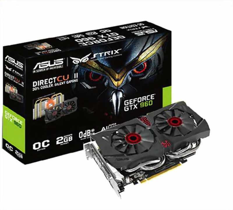 It gives the graphics card a thorough evaluation under various load, providing four separate benchmarks for Direct3D versions 9, 10, 11 and 12 (the last being done in 4K resolution if possible), and few more tests engaging DirectCompute capabilities.
Benchmark coverage: 26%
R9 370
4722
3DMark Fire Strike Graphics
Fire Strike is a DirectX 11 benchmark for gaming PCs. It features two separate tests displaying a fight between a humanoid and a fiery creature seemingly made of lava. Using 1920×1080 resolution, Fire Strike shows off some realistic enough graphics and is quite taxing on hardware.
Benchmark coverage: 14%
R9 370
5249
Mining hashrates
Cryptocurrency mining performance of Radeon R9 370. Usually measured in megahashes per second.
| Bitcoin / BTC (SHA256) | 336 Mh/s |
Game benchmarks
Let’s see how good Radeon R9 370 is for gaming. Particular gaming benchmark results are measured in frames per second. Comparisons with game system requirements are included, but remember that sometimes official requirements may reflect reality inaccurately.
Average FPS
Here are the average frames per second in a large set of popular modern games across different resolutions:
| Full HD | 45 |
Popular games
Relative perfomance
Overall Radeon R9 370 performance compared to nearest competitors among desktop video cards.
NVIDIA GeForce GTX 760
101.12
AMD Radeon HD 7950
100.93
AMD Radeon Sky 500
100.31
AMD Radeon R9 370
100
NVIDIA GeForce GTX 1630
98.88
AMD Radeon HD 7870
98. 82
82
NVIDIA GeForce GTX 580
95.71
Conclusion
Radeon R9 370 is a middle-level video card based on an outdated GCN 1.0 core and released only in OEM variant, so it never was actually sold directly to end users.
Some video FPS benchmarks:
NVIDIA equivalent
We believe that the nearest equivalent to Radeon R9 370 from NVIDIA is GeForce GTX 1630, which is slower by 1% and lower by 4 positions in our rating.
GeForce GTX
1630
Compare
Here are some closest NVIDIA rivals to Radeon R9 370:
NVIDIA GeForce GTX 670
112
NVIDIA GeForce GTX 1050
107.4
NVIDIA GeForce GTX 760
101. 12
12
AMD Radeon R9 370
100
NVIDIA GeForce GTX 1630
98.88
NVIDIA GeForce GTX 580
95.71
NVIDIA P104-100
94.22
Similar GPUs
Here is our recommendation of several graphics cards that are more or less close in performance to the one reviewed.
Radeon Sky
500
Compare
Radeon HD
7870 XT
Compare
P104
100
Compare
Radeon R9
270
Compare
GeForce GTX
670
Compare
GeForce GTX
760 Ti OEM
Compare
Recommended processors
These processors are most commonly used with Radeon R9 370 according to our statistics.
Xeon E5
2650 v2
3.4%
Core i3
10100F
3.2%
FX
6300
2.6%
Xeon E5
2420
2.1%
Core i5
3470
2%
Xeon E5
2689
1.8%
Ryzen 3
1200
1.6%
Xeon E5
2620 v3
1. 6%
6%
Core i5
4460
1.5%
Core i5
10400F
1.5%
User rating
Here you can see the user rating of the graphics card, as well as rate it yourself.
Questions and comments
Here you can ask a question about Radeon R9 370, agree or disagree with our judgements, or report an error or mismatch.
Please enable JavaScript to view the comments powered by Disqus.
GPU Compare | Graphics Card Comparison
The Radeon R9 370 will run 89% of the top 10,000 PC games. It will also run 63% of these games at the recommended or best experience levels.
- Manufacturer
-
AMD - Generation
- 9 generations old
- Category
-
High Performance - Dedicated RAM
-
2. 0 GB
0 GB - DirectX
-
12 - Rank
-
85th percentile of AMD GPUs - Rank in Power
-
74th of AMD GPUs - Rank in Popularity
-
202nd of AMD GPUs
Can the Radeon R9 370 run the Top PC games? You can see a GPU comparison by choosing another video card. How many games can your GPU run?
|
Radeon R9 370
|
Radeon RX 6950 XT
|
||
|---|---|---|---|
| Rank | Game |
|
|
| 1 |
Cyberpunk 2077 |
|
|
| 2 |
Grand Theft Auto V |
|
|
| 3 |
VALORANT |
|
|
| 4 |
Call of Duty: Warzone |
|
|
| 5 |
Elden Ring |
|
|
| 6 |
Marvel’s Spider-Man Remastered |
|
|
| 7 |
Red Dead Redemption 2 |
|
|
| 8 |
Call of Duty: Modern Warfare II |
|
|
| 9 |
God of War |
|
|
| 10 |
Fortnite |
|
|
| 11 |
FIFA 23 |
|
|
| 12 |
Minecraft |
|
|
| 13 |
The Witcher 3: Wild Hunt |
|
|
| 14 |
Apex Legends |
|
|
| 15 |
Forza Horizon 5 |
|
|
| 16 |
Genshin Impact |
|
|
| 17 |
League of Legends |
|
|
| 18 |
Assassin’s Creed Valhalla |
|
|
| 19 |
Counter-Strike: Global Offensive |
|
|
| 20 |
The Sims 4 |
|
|
| 21 |
FIFA 22 |
|
|
| 22 |
PLAYERUNKNOWN’S BATTLEGROUNDS |
|
|
| 23 |
Battlefield 2042 |
|
|
| 24 |
Far Cry 6 |
|
|
| 25 |
WARZONE |
|
|
| 26 |
1982 |
|
|
| 27 |
Dying Light 2 Stay Human |
|
|
| 28 |
GRID Autosport |
|
|
| 29 |
Call of Duty: Modern Warfare |
|
|
| 30 |
Horizon Zero Dawn |
|
|
| 31 |
ARK: Survival Evolved |
|
|
| 32 |
Assassin’s Creed: Origins |
|
|
| 33 |
Phasmophobia |
|
|
| 34 |
Grand Theft Auto IV |
|
|
| 35 |
Escape from Tarkov |
|
|
| 36 |
Devil May Cry 5 |
|
|
| 37 |
Days Gone |
|
|
| 38 |
Battlefield 1 |
|
|
| 39 |
Sea of Thieves |
|
|
| 40 |
Battlefield 5 |
|
|
| 41 |
Assassin’s Creed Odyssey |
|
|
| 42 |
Battlefield 4 |
|
|
| 43 |
Assassin’s Creed Unity |
|
|
| 44 |
NotGTAV |
|
|
| 45 |
Call of Duty: WW2 |
|
|
| 46 |
Hogwarts Legacy |
|
|
| 47 |
Rust |
|
|
| 48 |
Forza Horizon 4 |
|
|
| 49 |
Monster Hunter: World |
|
|
| 50 |
Fallout 4 |
|
|
| 51 |
Overwatch |
|
|
| 52 |
Dota 2 |
|
|
| 53 |
Call of Duty: Black Ops II |
|
|
| 54 |
UNCHARTED Legacy of Thieves Collection |
|
|
| 55 |
Assassin’s Creed IV Black Flag |
|
|
| 56 |
Tom Clancy’s Rainbow Six: Siege |
|
|
| 57 |
Rocket League |
|
|
| 58 |
Fall Guys: Ultimate Knockout |
|
|
| 59 |
SEKIRO: SHADOWS DIE TWICE |
|
|
| 60 |
Deathloop |
|
|
| 61 |
Destiny 2 |
|
|
| 62 |
Fortnite: Battle Royale |
|
|
| 63 |
Team Fortress 2 |
|
|
| 64 |
The Elder Scrolls V: Skyrim |
|
|
| 65 |
Metal Gear Rising: Revengeance |
|
|
| 66 |
Dark Souls 3 |
|
|
| 67 |
Return to Monkey Island |
|
|
| 68 |
GTA 5 Thor Mod |
|
|
| 69 |
PUBG Lite |
|
|
| 70 |
Far Cry 5 |
|
|
| 71 |
MONSTER HUNTER RISE |
|
|
| 72 |
Call of Duty: Modern Warfare 3 |
|
|
| 73 |
Assassin’s Creed III |
|
|
| 74 |
GTA 5 Premium Online Edition |
|
|
| 75 |
Stray |
|
|
| 76 |
Far Cry 3 |
|
|
| 77 |
Assetto Corsa |
|
|
| 78 |
Assassin’s Creed Syndicate |
|
|
| 79 |
Assassin’s Creed |
|
|
| 80 |
Call of Duty: Black Ops III |
|
|
| 81 |
The Forest |
|
|
| 82 |
Batman: Arkham Knight |
|
|
| 83 |
Civilization 6 |
|
|
| 84 |
GUNDAM EVOLUTION |
|
|
| 85 |
Tekken 7 |
|
|
| 86 |
Far Cry 4 |
|
|
| 87 |
Assassin’s Creed Rogue |
|
|
| 88 |
DayZ |
|
|
| 89 |
Assassin’s Creed II |
|
|
| 90 |
Age of Empires 4 |
|
|
| 91 |
Dead by Daylight |
|
|
| 92 |
Watch Dogs 2 |
|
|
| 93 |
Arma III |
|
|
| 94 |
Forza Horizon 3 |
|
|
| 95 |
Dying Light |
|
|
| 96 |
Cities: Skylines |
|
|
| 97 |
Warframe |
|
|
| 98 |
Terraria |
|
|
| 99 |
Project Zomboid |
|
|
| 100 |
Watch Dogs |
|
|
 ..
..
AMD
NVIDIA
Intel
| Rank | GPU |
|---|---|
AMD Radeon R9 370 — review.
 GPU Benchmark & Specs
AMD Radeon R9 370 graphics card (also called GPU) comes in 208 in the performance rating. It is a good result. The graphics card AMD Radeon R9 370 runs with the minimal clock speed 925 MHz. It is featured by the acceleration option and able to run up to 975 MHz. The manufacturer has equipped AMD with GB of 2 GB memory, clock speed 5600 MHz and bandwidth 179.2 GB/s.
The power consumption of the graphics card is 110 Watt, and the fabrication process is only 28 nm. Below you will find the main data on the compatibility, sizes, technologies and gaming performance test results. Also you can read and leave the comments.
Let’s take a closer look at the most important specifications of the graphics card. To have a good idea what a graphics card is the best, we recommend to use comparison service.
4.6
Out of 14
Hitesti score
Popular graphics cards
Most viewed
AMD Radeon RX Vega 7
Intel UHD Graphics 630
Intel UHD Graphics 600
NVIDIA Quadro T1000
AMD Radeon RX Vega 10
NVIDIA GeForce MX330
Intel HD Graphics 530
Intel UHD Graphics 620
Intel HD Graphics 4600
Intel HD Graphics 520
Buy here:
AliExpress
General info
The basic set of information will help you find out the graphics card AMD Radeon R9 370 release date and its purpose (laptops or PCs), as well as the price at the time of the release and the average current price. This data also includes the architecture employed by the producer, and the chip’s codename.
| Place in performance rating: | 267 | |||
| Architecture: | GCN 1.0 | |||
| Code name: | Trinidad | |||
| Type: | Desktop | |||
| Release date: | 5 May 2015 (6 years ago) | |||
| Price now: | $248 | |||
| Value for money: | 13.35 | |||
| GPU code name: | Trinidad | |||
| Market segment: | Desktop | |||
Technical specs
This is the important information that defines the graphics card’s capacity. The simpler the device production process, the better. The core’s power frequency is responsible for its speed (direct correlation) while the elaboration of signals is performed by the transistors (the more transistors, the faster the computations are carried out).
| Pipelines: | 1280 | |||
| Core clock speed: | 925 MHz | |||
| Boost Clock: | 975 MHz | |||
| Transistor count: | 2,800 million | |||
| Manufacturing process technology: | 28 nm | |||
| Power consumption (TDP): | 110 Watt | |||
| Texture fill rate: | 78. 00 00 |
|||
| Floating-point performance: | 2,496 gflops | |||
| Pipelines / CUDA cores: | 1280 | |||
| Boost clock speed: | 975 MHz | |||
| Number of transistors: | 2,800 million | |||
| Thermal design power (TDP): | 110 Watt | |||
Compatibility, dimensions and requirements
Today there are numerous form factors for PC cases, so it is extremely important to know the length of the graphics card and the types of its connection. This will help facilitate the upgrade process.
| Interface: | PCIe 3.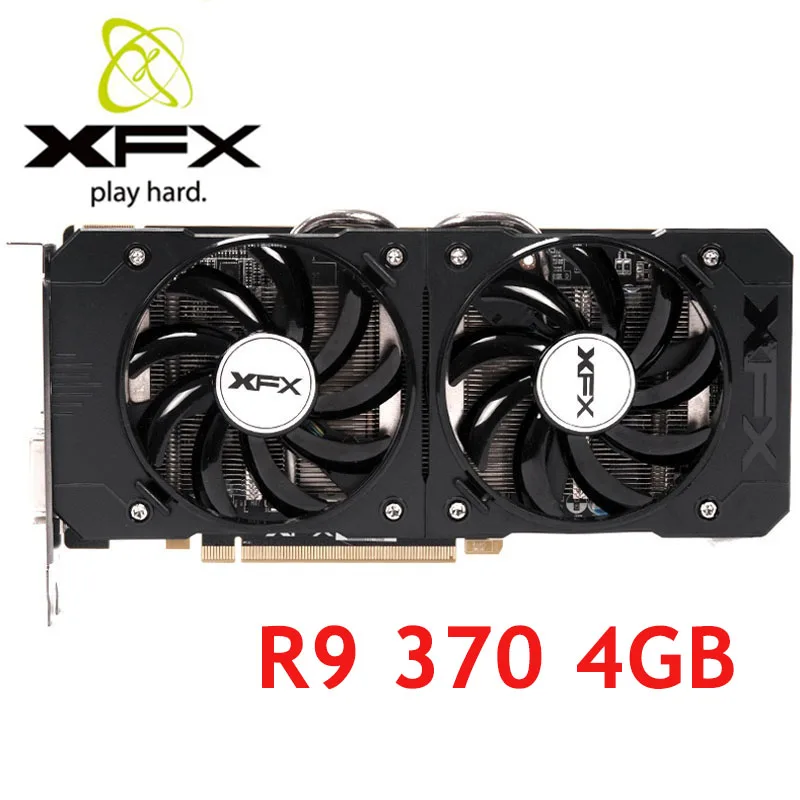 0 x16 0 x16 |
|||
| Length: | 221 mm | |||
| Supplementary power connectors: | 1x 6-pin | |||
Memory
The internal main memory is used for storing data while conducting computations. Contemporary games and professional graphic apps have high requirements for the memory’s volume and capacity. The higher this parameter, the more powerful and fast the graphics card is. Type of memory, the capacity and bandwidth for AMD Radeon R9 370.
| Memory type: | GDDR5 | |||
| Maximum RAM amount: | 2 GB | |||
| Memory bus width: | 256 Bit | |||
| Memory clock speed: | 5600 MHz | |||
| Memory bandwidth: | 179. 2 GB/s 2 GB/s |
|||
Video outputs and ports
As a rule, all contemporary graphics cards feature several connection types and additional ports. Knowing these peculiarities is crucial for avoiding problems with connecting the graphics card to the monitor or other peripheral devices.
| Display Connectors: | 2x DVI, 1x HDMI, 1x DisplayPort | |||
| HDMI: | + | |||
API support
All API-supported AMD Radeon R9 370 are listed below.
| DirectX: | 12 (11_1) | |||
| OpenGL: | 4.6 | |||
Overall gaming performance
All tests have been based on FPS counter. Let’s have a look on what place AMD Radeon R9 370 has been taken in the gaming performance test (calculation has been made in accordance with the game developer recommendations about system requirements; it can differ from the real world situations).
Select games to view
Horizon Zero DawnDeath StrandingF1 2020Gears TacticsDoom EternalHunt ShowdownEscape from TarkovHearthstoneRed Dead Redemption 2Star Wars Jedi Fallen OrderNeed for Speed HeatCall of Duty Modern Warfare 2019GRID 2019Ghost Recon BreakpointFIFA 20Borderlands 3ControlF1 2019League of LegendsTotal War: Three KingdomsRage 2Anno 1800The Division 2Dirt Rally 2.0AnthemMetro ExodusFar Cry New DawnApex LegendsJust Cause 4Darksiders IIIFarming Simulator 19Battlefield VFallout 76Hitman 2Call of Duty Black Ops 4Assassin´s Creed OdysseyForza Horizon 4FIFA 19Shadow of the Tomb RaiderStrange BrigadeF1 2018Monster Hunter WorldThe Crew 2Far Cry 5World of Tanks enCoreX-Plane 11.11Kingdom Come: DeliveranceFinal Fantasy XV BenchmarkFortniteStar Wars Battlefront 2Need for Speed PaybackCall of Duty WWIIAssassin´s Creed OriginsWolfenstein II: The New ColossusDestiny 2ELEXThe Evil Within 2Middle-earth: Shadow of WarFIFA 18Ark Survival EvolvedF1 2017Playerunknown’s Battlegrounds (2017)Team Fortress 2Dirt 4Rocket LeaguePreyMass Effect AndromedaGhost Recon WildlandsFor HonorResident Evil 7Dishonored 2Call of Duty Infinite WarfareTitanfall 2Farming Simulator 17Civilization VIBattlefield 1Mafia 3Deus Ex Mankind DividedMirror’s Edge CatalystOverwatchDoomAshes of the SingularityHitman 2016The DivisionFar Cry PrimalXCOM 2Rise of the Tomb RaiderRainbow Six SiegeAssassin’s Creed SyndicateStar Wars BattlefrontFallout 4Call of Duty: Black Ops 3Anno 2205World of WarshipsDota 2 RebornThe Witcher 3Dirt RallyGTA VDragon Age: InquisitionFar Cry 4Assassin’s Creed UnityCall of Duty: Advanced WarfareAlien: IsolationMiddle-earth: Shadow of MordorSims 4Wolfenstein: The New OrderThe Elder Scrolls OnlineThiefX-Plane 10.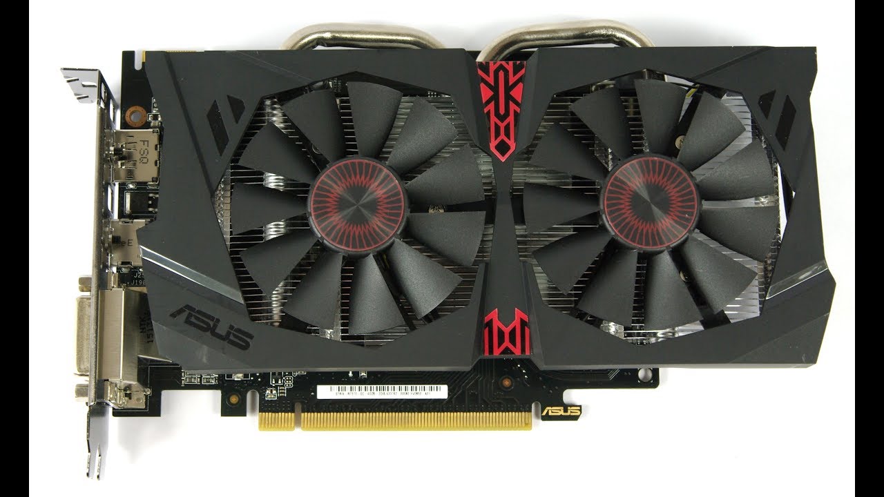 25Battlefield 4Total War: Rome IICompany of Heroes 2Metro: Last LightBioShock InfiniteStarCraft II: Heart of the SwarmSimCityTomb RaiderCrysis 3Hitman: AbsolutionCall of Duty: Black Ops 2World of Tanks v8Borderlands 2Counter-Strike: GODirt ShowdownDiablo IIIMass Effect 3The Elder Scrolls V: SkyrimBattlefield 3Deus Ex Human RevolutionStarCraft 2Metro 2033Stalker: Call of PripyatGTA IV — Grand Theft AutoLeft 4 DeadTrackmania Nations ForeverCall of Duty 4 — Modern WarfareSupreme Commander — FA BenchCrysis — GPU BenchmarkWorld in Conflict — BenchmarkHalf Life 2 — Lost Coast BenchmarkWorld of WarcraftDoom 3Quake 3 Arena — TimedemoHalo InfiniteFarming Simulator 22Battlefield 2042Forza Horizon 5Riders RepublicGuardians of the GalaxyBack 4 BloodDeathloopF1 2021Days GoneResident Evil VillageHitman 3Cyberpunk 2077Assassin´s Creed ValhallaDirt 5Watch Dogs LegionMafia Definitive EditionCyberpunk 2077 1.5GRID LegendsDying Light 2Rainbow Six ExtractionGod of War
low
1280×720
med.
1920×1080
high
1920×1080
ultra
1920×1080
QHD
2560×1440
4K
3840×2160
Horizon Zero Dawn (2020)
low
1280×720
med.
1920×1080
high
1920×1080
ultra
1920×1080
QHD
2560×1440
4K
3840×2160
Death Stranding (2020)
low
1280×720
med.
1920×1080
high
1920×1080
ultra
1920×1080
QHD
2560×1440
4K
3840×2160
F1 2020 (2020)
low
1280×720
med.
1920×1080
high
1920×1080
ultra
1920×1080
QHD
2560×1440
4K
3840×2160
Gears Tactics (2020)
low
1280×720
med.
1920×1080
high
1920×1080
ultra
1920×1080
QHD
2560×1440
4K
3840×2160
Doom Eternal (2020)
low
1280×720
med.
1920×1080
high
1920×1080
ultra
1920×1080
QHD
2560×1440
4K
3840×2160
| Legend | |
| 5 | Stutter – The performance of this graphics cards with this game is not well explored yet. According to interpolated information obtained from graphics cards of similar efficiency levels, the game is likely to stutter and show low frame rates. |
| May Stutter – The performance of this graphics cards with this game is not well explored yet. According to interpolated information obtained from graphics cards of similar efficiency levels, the game is likely to stutter and show low frame rates. | |
| 30 | Fluent – According to all known benchmarks with the specified graphical settings, this game is expected to run at 25fps or more |
| 40 | Fluent – According to all known benchmarks with the specified graphical settings, this game is expected to run at 35fps or more |
| 60 | Fluent – According to all known benchmarks with the specified graphical settings, this game is expected to run at 58fps or more |
May Run Fluently – The performance of this graphics cards with this game is not well explored yet. According to interpolated information obtained from graphics cards of similar efficiency levels, the game is likely to show fluent frame rates. According to interpolated information obtained from graphics cards of similar efficiency levels, the game is likely to show fluent frame rates. |
|
| ? | Uncertain – The testing of this graphics cards on this game showed unexpected results. A slower card might be able to produce higher and more consistent frame rates when running the same benchmark scene. |
| Uncertain – The performance of this graphics cards with this game is not well explored yet. No reliable data interpolation can be made based on the performance of similar cards of the same category. | |
| The value in the fields reflects the average frame rate across the entire database. To obtain individual results, move your cursor over the value. | |
Benchmark
Benchmarks help determine the performance in standard tests for AMD Radeon R9 370. We have listed the world’s most famous benchmarks so that you could obtain accurate results in each (see the description). Graphics card preliminary testing is especially important in the presence of high loads so that the user could see to what extent the graphic processing unit copes with computations and data elaboration.
Overall benchmark performance
NVIDIA GeForce GTX 760
21.93%
AMD Radeon HD 6990M Crossfire
21.93%
AMD Radeon R9 370
21.87%
AMD Radeon Pro Vega 16
21.68%
AMD Radeon HD 7870
21.38%
PassMark is a great benchmark that gets updated regularly and shows relevant information on the graphics card’s performance.
AMD Radeon HD 7950
NVIDIA GeForce GTX 760
AMD Radeon R9 370
AMD Radeon Pro Vega 16
AMD Radeon HD 7870
4. 6
6
Out of 14
Hitesti score
Share on social network:
In order to leave a review you need to log in
Reviews of AMD Radeon R9 370
Compare AMD Radeon R9 370
VS
NVIDIA GeForce GTX 1650
NVIDIA GeForce GTX 760
NVIDIA GeForce GTX 1050 Ti
AMD Radeon RX 560
NVIDIA GeForce GTX 960
NVIDIA GeForce GTX 1050 Ti
AMD Radeon R9 280
NVIDIA GeForce GTX 680M
Intel HD Graphics P530
AMD Fiji
AMD Radeon R7 370 vs AMD Radeon R9 280: What is the difference?
44points
AMD Radeon R7 370
37points
AMD Radeon R9 280
Comparison winner
vs
54 facts in comparison
AMD Radeon R7 370
AMD Radeon R9 280
Why is AMD Radeon R7 370 better than AMD Radeon R9 280?
- 98MHz faster GPU clock speed?
925MHzvs827MHz - 3.
 1 GPixel/s higher pixel rate?
29.6 GPixel/svs26.5 GPixel/s - 90W lower TDP?
110Wvs200W - 150MHz faster memory clock speed?
1400MHzvs1250MHz - 600MHz higher effective memory clock speed?
5600MHzvs5000MHz - 0.8 newer version of DirectX?
12vs11.2 - 0.8 newer version of OpenCL?
2vs1.2 - Has Double Precision Floating Point (DPFP)?
Why is AMD Radeon R9 280 better than AMD Radeon R7 370?
- 1.07 TFLOPS higher floating-point performance?
2.96 TFLOPSvs1.89 TFLOPS - 33.4 GTexels/s higher texture rate?
92.6 GTexels/svs59.2 GTexels/s - 1.5x more VRAM?
3GBvs2GB - 61GB/s more memory bandwidth?
240GB/svs179GB/s - 128bit wider memory bus width?
384bitvs256bit - 768 more shading units?
1792vs1024 - 1513million more transistors?
4313 millionvs2800 million - 48 more texture mapping units (TMUs)?
112vs64
Which are the most popular comparisons?
AMD Radeon R7 370
vs
AMD Radeon RX 550
AMD Radeon R9 280
vs
AMD Radeon R9 280X
AMD Radeon R7 370
vs
AMD Radeon R9 270X
AMD Radeon R9 280
vs
Gigabyte Radeon RX 550
AMD Radeon R7 370
vs
AMD Radeon R9 370X
AMD Radeon R9 280
vs
AMD Radeon RX 570
AMD Radeon R7 370
vs
Nvidia GeForce GTX 1050
AMD Radeon R9 280
vs
AMD Radeon Vega 8
AMD Radeon R7 370
vs
MSI GeForce GTX 980 Armor 2X OC
AMD Radeon R9 280
vs
Nvidia GeForce GTX 750 Ti
AMD Radeon R7 370
vs
MSI GeForce GTX 1050 Ti
AMD Radeon R9 280
vs
AMD Radeon RX 470
AMD Radeon R7 370
vs
AMD Radeon RX 470
AMD Radeon R9 280
vs
Gigabyte GeForce GTX 1050 Ti
AMD Radeon R7 370
vs
Nvidia GeForce GTX 750 Ti
AMD Radeon R9 280
vs
Nvidia GeForce GTX 960
AMD Radeon R7 370
vs
Nvidia GeForce GTX 960
AMD Radeon R9 280
vs
Nvidia GeForce MX330
AMD Radeon R7 370
vs
AMD Radeon R5
Price comparison
User reviews
Overall Rating
AMD Radeon R7 370
1 User reviews
AMD Radeon R7 370
5. 0/10
0/10
1 User reviews
AMD Radeon R9 280
0 User reviews
AMD Radeon R9 280
0.0/10
0 User reviews
Features
Value for money
5.0/10
1 votes
No reviews yet
Gaming
5.0/10
1 votes
No reviews yet
Performance
5.0/10
1 votes
No reviews yet
Fan noise
10.0/10
1 votes
No reviews yet
Reliability
6.0/10
1 votes
No reviews yet
Performance
1.GPU clock speed
925MHz
827MHz
The graphics processing unit (GPU) has a higher clock speed.
2.GPU turbo
975MHz
933MHz
When the GPU is running below its limitations, it can boost to a higher clock speed in order to give increased performance.
3.pixel rate
29.6 GPixel/s
26. 5 GPixel/s
The number of pixels that can be rendered to the screen every second.
4.floating-point performance
1.89 TFLOPS
2.96 TFLOPS
Floating-point performance is a measurement of the raw processing power of the GPU.
5.texture rate
59.2 GTexels/s
92.6 GTexels/s
The number of textured pixels that can be rendered to the screen every second.
6.GPU memory speed
1400MHz
1250MHz
The memory clock speed is one aspect that determines the memory bandwidth.
7.shading units
Shading units (or stream processors) are small processors within the graphics card that are responsible for processing different aspects of the image.
8.texture mapping units (TMUs)
TMUs take textures and map them to the geometry of a 3D scene. More TMUs will typically mean that texture information is processed faster.
9.render output units (ROPs)
The ROPs are responsible for some of the final steps of the rendering process, writing the final pixel data to memory and carrying out other tasks such as anti-aliasing to improve the look of graphics.
Memory
1.effective memory speed
5600MHz
5000MHz
The effective memory clock speed is calculated from the size and data rate of the memory. Higher clock speeds can give increased performance in games and other apps.
2.maximum memory bandwidth
179GB/s
240GB/s
This is the maximum rate that data can be read from or stored into memory.
3.VRAM
VRAM (video RAM) is the dedicated memory of a graphics card. More VRAM generally allows you to run games at higher settings, especially for things like texture resolution.
4.memory bus width
256bit
384bit
A wider bus width means that it can carry more data per cycle. It is an important factor of memory performance, and therefore the general performance of the graphics card.
5.version of GDDR memory
Newer versions of GDDR memory offer improvements such as higher transfer rates that give increased performance.
6.Supports ECC memory
✖AMD Radeon R7 370
✖AMD Radeon R9 280
Error-correcting code memory can detect and correct data corruption. It is used when is it essential to avoid corruption, such as scientific computing or when running a server.
Features
1.DirectX version
DirectX is used in games, with newer versions supporting better graphics.
2.OpenGL version
OpenGL is used in games, with newer versions supporting better graphics.
3.OpenCL version
Some apps use OpenCL to apply the power of the graphics processing unit (GPU) for non-graphical computing. Newer versions introduce more functionality and better performance.
4.Supports multi-display technology
✔AMD Radeon R7 370
✔AMD Radeon R9 280
The graphics card supports multi-display technology. This allows you to configure multiple monitors in order to create a more immersive gaming experience, such as having a wider field of view.
5.load GPU temperature
Unknown. Help us by suggesting a value. (AMD Radeon R7 370)
Unknown. Help us by suggesting a value. (AMD Radeon R9 280)
A lower load temperature means that the card produces less heat and its cooling system performs better.
6.supports ray tracing
✖AMD Radeon R7 370
✖AMD Radeon R9 280
Ray tracing is an advanced light rendering technique that provides more realistic lighting, shadows, and reflections in games.
7.Supports 3D
✔AMD Radeon R7 370
✔AMD Radeon R9 280
Allows you to view in 3D (if you have a 3D display and glasses).
8.supports DLSS
✖AMD Radeon R7 370
✖AMD Radeon R9 280
DLSS (Deep Learning Super Sampling) is an upscaling technology powered by AI. It allows the graphics card to render games at a lower resolution and upscale them to a higher resolution with near-native visual quality and increased performance. DLSS is only available on select games.
9.PassMark (G3D) result
Unknown. Help us by suggesting a value. (AMD Radeon R9 280)
This benchmark measures the graphics performance of a video card. Source: PassMark.
Ports
1.has an HDMI output
✔AMD Radeon R7 370
✔AMD Radeon R9 280
Devices with a HDMI or mini HDMI port can transfer high definition video and audio to a display.
2.HDMI ports
Unknown. Help us by suggesting a value. (AMD Radeon R9 280)
More HDMI ports mean that you can simultaneously connect numerous devices, such as video game consoles and set-top boxes.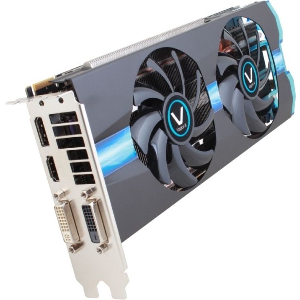
3.HDMI version
Unknown. Help us by suggesting a value. (AMD Radeon R7 370)
Unknown. Help us by suggesting a value. (AMD Radeon R9 280)
Newer versions of HDMI support higher bandwidth, which allows for higher resolutions and frame rates.
4.DisplayPort outputs
Unknown. Help us by suggesting a value. (AMD Radeon R9 280)
Allows you to connect to a display using DisplayPort.
5.DVI outputs
Allows you to connect to a display using DVI.
6.mini DisplayPort outputs
Allows you to connect to a display using mini-DisplayPort.
Price comparison
Cancel
Which are the best graphics cards?
AMD Radeon R9 370 review: GPU specs, performance benchmarks
Buy on Amazon
Radeon R9 370 videocard released by AMD; release date: 5 May 2015. The videocard is designed for desktop-computers and based on GCN 1.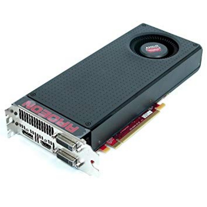 0 microarchitecture codenamed Trinidad.
Core clock speed — 925 MHz. Boost clock speed — 975 MHz. Texture fill rate — 78 GTexel / s. Pipelines — 1280. Floating-point performance — 2,496 gflops. Manufacturing process technology — 28 nm. Transistors count — 2,800 million. Power consumption (TDP) — 110 Watt.
Memory type: GDDR5. Maximum RAM amount — 2 GB. Memory bus width — 256 Bit. Memory clock speed — 5600 MHz. Memory bandwidth — 179.2 GB / s.
Benchmarks
| PassMark G3D Mark |
|
|
||||
| PassMark G2D Mark |
|
|
||||
| Geekbench OpenCL |
|
|
||||
CompuBench 1.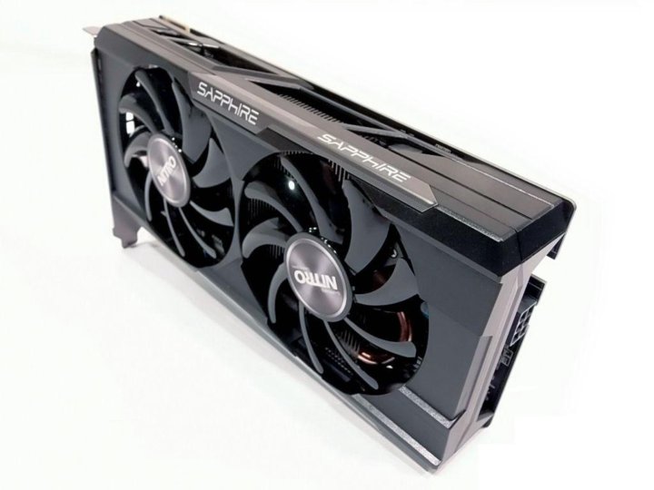 5 Desktop 5 DesktopFace Detection |
|
|
||||
| CompuBench 1.5 Desktop Bitcoin Mining |
|
|
||||
| GFXBench 4.0 Car Chase Offscreen |
|
|
||||
GFXBench 4.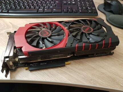 0 0Manhattan |
|
|
||||
| GFXBench 4.0 T-Rex |
|
|
||||
| GFXBench 4.0 Car Chase Offscreen |
|
|
||||
| GFXBench 4.0 Manhattan |
|
|
||||
| GFXBench 4.0 T-Rex |
|
|
||||
| 3DMark Fire Strike Graphics Score |
|
|
 000 Fps
| Name | Value |
|---|---|
| PassMark — G3D Mark | 4722 |
| PassMark — G2D Mark | 781 |
| Geekbench — OpenCL | 75346 |
CompuBench 1.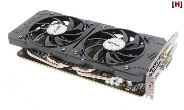 5 Desktop — Face Detection 5 Desktop — Face Detection |
64.576 mPixels/s |
| CompuBench 1.5 Desktop — Bitcoin Mining | 336.491 mHash/s |
| GFXBench 4.0 — Car Chase Offscreen | 6096 Frames |
| GFXBench 4.0 — Manhattan | 3718 Frames |
| GFXBench 4.0 — T-Rex | 3357 Frames |
| GFXBench 4.0 — Car Chase Offscreen | 6096.000 Fps |
| GFXBench 4.0 — Manhattan | 3718.000 Fps |
| GFXBench 4.0 — T-Rex | 3357.000 Fps |
| 3DMark Fire Strike — Graphics Score | 0 |
Specifications (specs)
| Architecture | GCN 1. 0 0 |
| Code name | Trinidad |
| Launch date | 5 May 2015 |
| Place in performance rating | 289 |
| Type | Desktop |
| Boost clock speed | 975 MHz |
| Core clock speed | 925 MHz |
| Floating-point performance | 2,496 gflops |
| Manufacturing process technology | 28 nm |
| Pipelines | 1280 |
| Texture fill rate | 78 GTexel / s |
| Thermal Design Power (TDP) | 110 Watt |
| Transistor count | 2,800 million |
|
|
|
| Display Connectors | 2x DVI, 1x HDMI, 1x DisplayPort |
| Interface | PCIe 3. 0 x16 0 x16 |
| Length | 221 mm |
| Supplementary power connectors | 1x 6-pin |
| DirectX | 12.0 (11_1) |
| OpenGL | 4.5 |
| Maximum RAM amount | 2 GB |
| Memory bandwidth | 179.2 GB / s |
| Memory bus width | 256 Bit |
| Memory clock speed | 5600 MHz |
| Memory type | GDDR5 |
Navigation
Choose a GPU
Compare videocards
Compare AMD Radeon R9 370 with others
AMD
Radeon R9 370
vs
ATI
Radeon X800 SE
AMD
Radeon R9 370
vs
ATI
Mobility Radeon HD 540v
AMD
Radeon R9 370
vs
AMD
Radeon HD 7990
AMD
Radeon R9 370
vs
AMD
Radeon RX 560X
AMD
Radeon R9 370
vs
AMD
Radeon RX 5500M
AMD
Radeon R9 370
vs
NVIDIA
Quadro T1000 Max-Q
Radeon R7 370 vs Radeon R9 370 Graphics cards Comparison
Find out if it is worth upgrading your current GPU setup by comparing Radeon R7 370 and Radeon R9 370.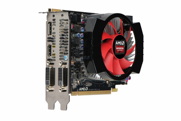 Here you can take a closer look at graphics cards specs, such as core clock speed, memory type and size, display connectors, etc. The price, overall benchmark and gaming performances are usually defining factors when it comes to choosing between Radeon R7 370 and Radeon R9 370. Make sure that the graphics card has compatible dimensions and will properly fit in your new or current computer case. Also these graphics cards may have different system power recommendations, so take that into consideration and upgrade your PSU if necessary.
Radeon R7 370
Check Price
Radeon R9 370
Main Specs
| Radeon R7 370 | Radeon R9 370 | |
| Power consumption (TDP) | 110 Watt | 110 Watt |
| Interface | PCIe 3. 0 x16 0 x16 |
PCIe 3.0 x16 |
| Supplementary power connectors | 1 x 6-pin | 1x 6-pin |
| Memory type | GDDR5 | GDDR5 |
| Maximum RAM amount | 4 GB | 2 GB |
| Display Connectors | 2x DVI, 1x HDMI, 1x DisplayPort | 2x DVI, 1x HDMI, 1x DisplayPort |
|
Check Price |
- Both graphics cards have the same power consumption of 110 Watt.
- Both video cards are using PCIe 3.0 x16 interface connection to a motherboard.
- Radeon R7 370 has 2 GB more memory, than Radeon R9 370.
- Both cards are used in Desktops.
- Radeon R7 370 and Radeon R9 370 are build with GCN 1.0 architecture.
- Radeon R7 370 and Radeon R9 370 are manufactured by 28 nm process technology.
- Radeon R9 370 is 69 mm longer, than Radeon R7 370.
- Memory clock speed of Radeon R9 370 is 4625 MHz higher, than Radeon R7 370.
Game benchmarks
| Assassin’s Creed OdysseyBattlefield 5Call of Duty: WarzoneCounter-Strike: Global OffensiveCyberpunk 2077Dota 2Far Cry 5FortniteForza Horizon 4Grand Theft Auto VMetro ExodusMinecraftPLAYERUNKNOWN’S BATTLEGROUNDSRed Dead Redemption 2The Witcher 3: Wild HuntWorld of Tanks | ||
| high / 1080p | 21−24 | 35−40 |
| ultra / 1080p | 14−16 | 21−24 |
| QHD / 1440p | 8−9 | 16−18 |
| 4K / 2160p | 5−6 | 10−11 |
| low / 720p | 40−45 | 60−65 |
| medium / 1080p | 27−30 | 40−45 |
| The average gaming FPS of Radeon R9 370 in Assassin’s Creed Odyssey is 60% more, than Radeon R7 370. |
||
| high / 1080p | 35−40 | 55−60 |
| ultra / 1080p | 30−35 | 45−50 |
| QHD / 1440p | 14−16 | 35−40 |
| 4K / 2160p | 9−10 | 18−20 |
| low / 720p | 75−80 | 100−110 |
| medium / 1080p | 40−45 | 60−65 |
| The average gaming FPS of Radeon R9 370 in Battlefield 5 is 54% more, than Radeon R7 370. | ||
| low / 768p | 50−55 | 50−55 |
| QHD / 1440p | 0−1 | 0−1 |
Radeon R7 370 and Radeon R9 370 have the same average FPS in Call of Duty: Warzone. |
||
| low / 768p | 230−240 | 250−260 |
| medium / 768p | 210−220 | 220−230 |
| ultra / 1080p | 130−140 | 180−190 |
| QHD / 1440p | 100−110 | 110−120 |
| 4K / 2160p | 55−60 | 70−75 |
| high / 768p | 170−180 | 210−220 |
| The average gaming FPS of Radeon R9 370 in Counter-Strike: Global Offensive is 15% more, than Radeon R7 370. | ||
| low / 768p | 60−65 | 60−65 |
| ultra / 1080p | 55−60 | − |
| medium / 1080p | 55−60 | 55−60 |
| Radeon R7 370 and Radeon R9 370 have the same average FPS in Cyberpunk 2077. |
||
| low / 768p | 120−130 | 120−130 |
| medium / 768p | 110−120 | 110−120 |
| ultra / 1080p | 85−90 | 100−110 |
| The average gaming FPS of Radeon R9 370 in Dota 2 is 5% more, than Radeon R7 370. | ||
| high / 1080p | 27−30 | 45−50 |
| ultra / 1080p | 24−27 | 40−45 |
| QHD / 1440p | 21−24 | 27−30 |
| 4K / 2160p | 9−10 | 14−16 |
| low / 720p | 55−60 | 80−85 |
| medium / 1080p | 30−33 | 45−50 |
The average gaming FPS of Radeon R9 370 in Far Cry 5 is 48% more, than Radeon R7 370. |
||
| high / 1080p | 35−40 | 60−65 |
| ultra / 1080p | 27−30 | 45−50 |
| QHD / 1440p | 16−18 | 27−30 |
| 4K / 2160p | − | 27−30 |
| low / 720p | 130−140 | 180−190 |
| medium / 1080p | 80−85 | 110−120 |
| The average gaming FPS of Radeon R9 370 in Fortnite is 45% more, than Radeon R7 370. | ||
| high / 1080p | 35−40 | 60−65 |
| ultra / 1080p | 27−30 | 45−50 |
| QHD / 1440p | 16−18 | 30−35 |
| 4K / 2160p | 14−16 | 24−27 |
| low / 720p | 75−80 | 100−110 |
| medium / 1080p | 40−45 | 65−70 |
The average gaming FPS of Radeon R9 370 in Forza Horizon 4 is 55% more, than Radeon R7 370. |
||
| low / 768p | 110−120 | 140−150 |
| medium / 768p | 100−105 | 120−130 |
| high / 1080p | 45−50 | 70−75 |
| ultra / 1080p | 18−20 | 30−35 |
| QHD / 1440p | 9−10 | 21−24 |
| The average gaming FPS of Radeon R9 370 in Grand Theft Auto V is 36% more, than Radeon R7 370. | ||
| high / 1080p | 14−16 | 24−27 |
| ultra / 1080p | 12−14 | 20−22 |
| QHD / 1440p | 10−12 | 16−18 |
| 4K / 2160p | 3−4 | 8−9 |
| low / 720p | 45−50 | 65−70 |
| medium / 1080p | 20−22 | 30−35 |
The average gaming FPS of Radeon R9 370 in Metro Exodus is 55% more, than Radeon R7 370. |
||
| low / 768p | 120−130 | 130−140 |
| medium / 1080p | 110−120 | 120−130 |
| The average gaming FPS of Radeon R9 370 in Minecraft is 8% more, than Radeon R7 370. | ||
| ultra / 1080p | 14−16 | 14−16 |
| low / 720p | 75−80 | 100−110 |
| medium / 1080p | 18−20 | 18−20 |
| The average gaming FPS of Radeon R9 370 in PLAYERUNKNOWN’S BATTLEGROUNDS is 24% more, than Radeon R7 370. | ||
| high / 1080p | 16−18 | 24−27 |
| ultra / 1080p | 10−12 | 16−18 |
| QHD / 1440p | 3−4 | 10−11 |
| 4K / 2160p | 2−3 | 7−8 |
| low / 720p | 40−45 | 65−70 |
| medium / 1080p | 21−24 | 35−40 |
The average gaming FPS of Radeon R9 370 in Red Dead Redemption 2 is 68% more, than Radeon R7 370. |
||
| low / 768p | 80−85 | 130−140 |
| medium / 768p | 50−55 | 85−90 |
| high / 1080p | 27−30 | 45−50 |
| ultra / 1080p | 16−18 | 24−27 |
| 4K / 2160p | 9−10 | 16−18 |
| The average gaming FPS of Radeon R9 370 in The Witcher 3: Wild Hunt is 63% more, than Radeon R7 370. | ||
| low / 768p | 90−95 | 90−95 |
| medium / 768p | 60−65 | 60−65 |
| ultra / 1080p | 40−45 | 50−55 |
| high / 768p | 55−60 | 60−65 |
The average gaming FPS of Radeon R9 370 in World of Tanks is 6% more, than Radeon R7 370. |
||
Full Specs
| Radeon R7 370 | Radeon R9 370 | |
| Architecture | GCN 1.0 | GCN 1.0 |
| Code name | Trinidad (Pitcairn) | Trinidad |
| Type | Desktop | Desktop |
| Release date | 5 May 2015 | 5 May 2015 |
| Pipelines | 1024 | 1280 |
| Core clock speed | 925 MHz | |
| Boost Clock | 975 MHz | 975 MHz |
| Transistor count | 2,800 million | 2,800 million |
| Manufacturing process technology | 28 nm | 28 nm |
| Texture fill rate | 62. 40 40 |
78.00 |
| Floating-point performance | 1,997 gflops | 2,496 gflops |
| Length | 152 mm | 221 mm |
| Memory bus width | 256 Bit | 256 Bit |
| Memory clock speed | 975 MHz | 5600 MHz |
| Memory bandwidth | 179.2 GB/s | 179.2 GB/s |
| Shared memory | — | |
| DirectX | 12 (11_1) | |
| Shader Model | 5.1 | 5.1 |
| OpenGL | 4.6 | 4.6 |
| OpenCL | 2.0 | 1.2 |
| Vulkan | + | 1.2.131 |
| Monero / XMR (CryptoNight) | 0. 42 kh/s 42 kh/s |
|
| FreeSync | + | |
| Bus support | PCIe 3.0 | |
| HDMI | + | |
| Bitcoin / BTC (SHA256) | 359 Mh/s | 336 Mh/s |
| Eyefinity | + | |
| TrueAudio | + | |
| Mantle | + | |
| Design | reference | |
| Number of Eyefinity displays | 6 | |
| DisplayPort support | + | |
| CrossFire | + | |
| VCE | + | |
| DDMA audio | + | |
| Decred / DCR (Decred) | 0.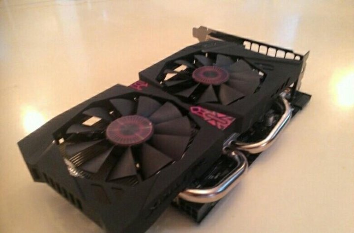 52 Gh/s 52 Gh/s |
|
| Ethereum / ETH (DaggerHashimoto) | 14 Mh/s | |
| Zcash / ZEC (Equihash) | 150 Sol/s | |
| AppAcceleration | + | |
|
Check Price |
Similar compares
- Radeon R7 370 vs P104 100
- Radeon R7 370 vs Radeon R9 M390X
- Radeon R9 370 vs P104 100
- Radeon R9 370 vs Radeon R9 M390X
- Radeon R7 370 vs Radeon HD 7950
- Radeon R7 370 vs GeForce GTX 670MX SLI
- Radeon R9 370 vs Radeon HD 7950
- Radeon R9 370 vs GeForce GTX 670MX SLI
AMD Radeon Video Card Families Reference
Radeon X
Family Reference
Radeon X1000 Family Reference
Radeon HD 2000 Family Reference
Radeon HD 4000 Family Reference
Radeon HD Family Reference 5000
Radeon HD 6000 Family Reference
Radeon HD 7000 Family Reference
Reference information about the family of video cards Radeon 200
Reference information on the family of video cards Radeon 300
Graphic processors specifications
| «Fiji» | «Hawaiii» | «Antigu» » | Trinidad Curacao Pitcairn |
Tobago Bonaire |
|||||||||||||||||||||
| base article | here | here | 0016 PSP, GB/C (bit) |
Textory- Call, GTEK |
PhILRIET, GPICS | TDP, W | |||||||||||||||||||
| Radeon R9 Fury | «Fiji» | 4096/259 9001 1050 | 1000 | 4 HBM | 512 (4096) | 269 | 67 | 275 | |||||||||||||||||
| Radeon R9 Fury | «Fiji» | 3584/224/64 | 1000 | 1000 | 4 HBM | 512 (4096) | 224 | 64 | 275 | ||||||||||||||||
| Radeon R9 Nano | «Fiji» | 4096/256/64 | 4 HBM | 4 HBM 4 HBM 4 HBM 4 HBM 4 HBM 4 HBM 4 HBM 4 HBM 4 HBM 4 HBM 4 HBM 4 HBM 4 Hbm | 64 | 175 | |||||||||||||||||||
| Radeon R9 390X | «Hawaii» | 2816/176/64 | 1050 | 1500(6000) | 8 GDDR5 | 384 (512) | 185 | 67 | 275 | ||||||||||||||||
| Radeon R9 390 | «Hawaii» | 2560/160/64 | 1000 | 1500(6000) | 8 GDDR5 | 384 (512) | 160 | 64 | 275 | ||||||||||||||||
| Radeon R9 380X | “Tonga” | 2048/128/32 | 970 | 1425 (5700) | 4 GDDR5 | 182 (256) | 124. 2 2
| 31.0 31.0 31.0 31.0 31. | Radeon R9 380 | «Tonga» | 1792/112/32 | 970 | 1425 (5700) | 2-4 GDDR5 | 182 (256) | 108.6 | 190 900 Pitcairn | 1024/64/32 | 975 | 1400 (5600) | 2-4 GDDR5 | (256) | 62.4 9001.2 | 110 | |
| Radaon 360 | Bonaire | 768/48/16 | 1050 | 1625 (6500) | 2 GDDR5 | 104 (128) | 50.4 | 16.8 | 100 |
Graphic accelerator AMD Radeon R9 Fury x
 6 floating point ALUs (integer and floating point formats supported, with FP32 and FP64 precision)
 67.0160033
With this model, AMD opened a new subfamily of elite Fury video cards nominally included in the Radeon 300 line.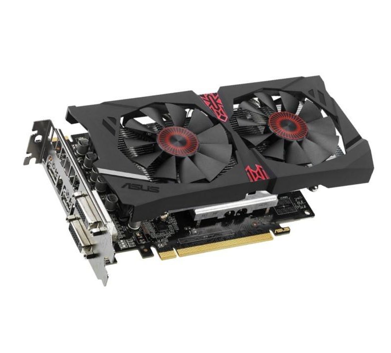 in this case, a single-chip) solution. The company did not try to justify the choice of the name Fury. Probably, this name was taken from the once successful video cards of the ATI Rage Fury family, released at the end of 2019.90s. In addition, the Furies are the goddesses of revenge in ancient Roman mythology, and the Titans are gods from ancient Greek mythology.
The Radeon R9 Fury X sits at the very top of the company’s product line, with a MSRP of $649 for the Radeon R9 Fury X, exactly on par with its direct competitor, Nvidia’s GeForce GTX 980 Ti, which was announced at the end of May. as a preemptive strike against the future (at that time) AMD solution. The competing solution offered performance close to that of the high-end GeForce GTX Titan X for much less money, and Fury X now has to compete with the gaming GTX 980 Ti.
One of the most controversial points in the characteristics of the new model is the presence of only 4 GB of video memory, which is enough even for high resolutions at maximum quality settings, but in a number of modern games with 4K rendering resolution, as well as full-screen anti-aliasing and high settings.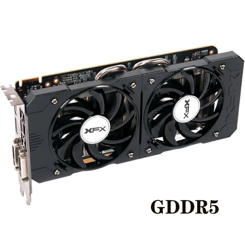 quality, even more volume is needed now. And AMD would be happy to offer an 8 GB option, but alas, the first generation of HBM memory simply does not allow it. Read more about all the subtleties associated with HBM memory below.
The graphics card itself is very compact — the Radeon R9 Fury X PCB is only 7.5 inches (about 190mm) long, well short of typical high-end reference cards. A small board is combined with a large water cooling system heatsink. The combination of CBO with HBM-memory made it possible to reduce the physical dimensions and the number of components on the board (in the power circuit, in particular). You can compare GPU and RAM areas on Radeon R9 290X and R9 Fury X:
Under typical gaming conditions, the Radeon R9 Fury X graphics card consumes about 275W, but since it is equipped with a pair of 8-pin PCI-E power connectors, it can draw up to 375W from the power supply, that is, much more. In terms of I / O interfaces, the Radeon R9 Fury X is capable of outputting information to six displays (using a DisplayPort 1. 2 MST hub) connected via DVI (adapter required), HDMI 1.4a and DisplayPort 1.2a.
Among the connectors on the board there is one HDMI video output and three DisplayPort. They decided to get rid of the outdated DVI connector altogether, although the Radeon HD 7970 and Radeon R9 290X they still were, and sometimes two. And users of older monitors with DVI interfaces will now have to use adapters: passive ones if Single Link is enough, and more expensive ones for Dual Link connections.
Alas, due to the lack of support for HDMI 2.0, the new product supports image output in 4K resolution at 60 Hz only via DisplayPort. It is likely that over time it will also be possible to use active adapters from DisplayPort to HDMI 2.0, but so far such configurations do not work.
Architectural and functional features
Since the Radeon R9 Fury X is based on the Fiji GPU, which belongs to the long-established Graphics Core Next (GCN) architecture, you can learn about many of the details in our early materials. This architecture is the basis of all modern AMD solutions, and even the latest GPUs differ only in some modifications in computing abilities and additional graphics capabilities that are important for DirectX 12 support.
Like the previous high-end Hawaii chip, the new GPU is not the first of a completely new architecture, but only uses the latest version of the current Graphics Core Next (it can be called GCN 1.2 or GCN third generation). Fiji has made a small number of changes compared to last year’s Tonga, and the novelty can be attributed to the GCN 1.2 generation. From the basic changes that have appeared in Fiji, based on the latest version of the Graphics Core Next architecture, we can note everything that we have already seen in the Tonga chip, which is based on the Radeon R9 model video card.285.
The new top-end graphics processor includes all the GCN 1.2 improvements, including improved geometry processing and tessellation performance (according to these indicators, Fiji is on par with Hawaii and Tonga and faster than Tahiti), new data compression methods without frame loss buffer, some multimedia 16-bit instructions, and increased L2 cache to 2 MB. In terms of computing power, the new GPU has received improved scheduling and task distribution, and several new instructions for parallel data processing.
The most «loud» architectural improvement is the appearance of significantly improved lossless framebuffer data compression algorithms — for this, the ROP blocks have been specially modified. It is the operations (mostly writes) with the frame buffer that are the most demanding on memory bandwidth, because the GPU writes a very large number of pixels to the buffer each frame. So an increase in the efficiency of this work leads to less demanding memory bandwidth and increases the so-called effective memory bandwidth.
In the case of GCN 1.2 architecture chips, new frame buffer data compression methods provide compression ratios up to 8:1, and on average this results in a 40% improvement in bandwidth efficiency. For example, the Radeon R9 285 with a 256-bit bus has a similar effective bandwidth to the Radeon R9 280 with a 384-bit memory bus. Well, in the case of the top-end Fiji chip, the effective memory bandwidth has grown to ultra-high values, since the chip contains 4096-bit HBM memory, but more on that later.
Also, as part of the GCN 1.2 architecture, some changes were made to the computing units: improvements in scheduling and distribution of tasks between execution units within the heterogeneous HSA architecture, the introduction of new 16-bit instructions to increase speed and reduce power consumption, as well as improvements in parallel processing data, which is most important in the case of the top Fiji GPU. Like other products of the GCN 1.2 architecture, the new GPU has limited data exchange capability between different SIMD lines, opening up the possibility for new efficient algorithms in OpenCL programs.
Well, for ordinary enthusiasts, the most important architectural changes were the already mentioned frame buffer data compression and acceleration of geometric processing and tessellation. This improvement was made back in Hawaii, nothing has changed in Tonga.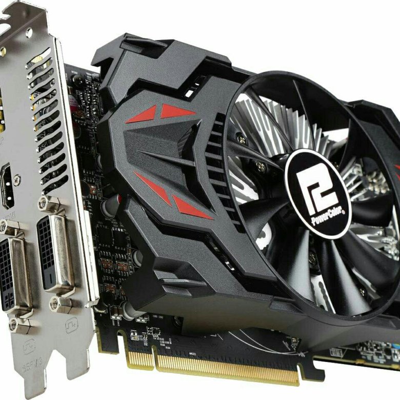 But now, in the case of Fiji, the operation of the geometry pipeline has been further optimized, which should have a positive effect in tasks with a large amount of geometry and using tessellation.
The general scheme of the Fiji GPU is very similar to the one we saw in the Hawaii chip, released back in 2013. Both of these GPUs are divided into four Shader Engines, each with its own geometry processor and rasterizer, as well as four larger ROPs capable of processing 16 pixels per clock (for a total of 64 ROPs in each of these chips). The GPU has a single command processor and eight Asynchronous Compute Engines, which have been modified to reflect the changes in GCN 1.2.
Compared to Hawaii, in terms of organization, AMD engineers did not touch anything in the Fiji chip, simply placing more Compute Units in each Shader Engine (16 instead of 11), but left the number of engines themselves unchanged (probably this is — an architectural limitation of GCN in its current form) and the number of other execution units in their composition.
Given that each CU contains 64 ALUs, there are 1024 ALUs per Shader Engine and 4096 stream processors for the whole of Fiji. Accordingly, the number of texture units was also increased, because for each CU in the video chips of the GCN architecture there are four TMUs, so there are 256 of them in the new GPU, unlike 176 TMUs in Hawaii.
Accordingly, the theoretical values of the speed of calculations and texture processing in Fiji increased, but the peak values of the speed of geometry processing and fill speed (fillrate, ROP performance) remained almost at the same level, adjusted only for different GPU frequencies. Perhaps, in some cases, there may be an emphasis on overall performance in the speed of filling the scene or processing geometry, but this greatly depends on the conditions (the complexity of the scene and the overdraw value for it, as well as the resolution and full-screen anti-aliasing, etc.).
But AMD representatives claim that in the case of Hawaii, memory bandwidth (LBW) is most often the limiter, and the performance of ROP units is quite enough in most cases, and the rendering speed is rarely limited by their capabilities. But after all, Fiji uses a faster HBM memory with a wide bus, as well as new data compression methods in the screen buffer, and the ROP blocks themselves in Fiji received more opportunities to work with 16-bit per color data. So, most likely, the number of cases of focusing the overall performance on the possibility of ROP units will only increase. And it was not possible to increase the number of ROP blocks in the new chip, since the GPU turned out to be quite large anyway.
Based on the number of ALUs of 4096 and the maximum GPU frequency of 1050 MHz, a theoretical single precision (FP32) performance of 8.6 teraflops can be obtained. But with double-precision calculations in the new chip, things are much worse than in the same Hawaii — here AMD had to go in about the same direction that Nvidia chose for its older Maxwell, shifting the focus towards gaming to the detriment of professional computing.
Although different GCN architecture chips can perform FP64 calculations at 1/2 to 1/16 of the speed of FP32 calculations, for Fiji, AMD chose the minimum value (1/16), which gives an FP64 speed of about 538 megaflops. Compare this to the capabilities of Hawaii, which performs double precision calculations only twice as fast as single precision calculations. Even less complex cheap GCN chips have 1/8 temp! So Fiji has become as “playable” as the GM200. It seems that AMD took a cue (good or not — depends on the point of view) with Nvidia trimming its top-end GPU even further. And in the end, both top gaming chips from AMD and Nvidia are more gaming than professional computing.
And otherwise, the Fiji GPU is not quite a typical video chip for AMD. This time the company released a rather large GPU — almost 600 mm in area 2 ! But for several years now they have been trying to avoid such large and super-hot video chips, since they are too expensive to develop and manufacture, and they require more time from the start of development to market entry due to the complexity and design and reduced yield of suitable chips. Not to mention that with larger GPUs, the risk of failure is higher. Although, of course, now the 28 nm process technology has already been perfectly developed and does not cause any special problems for video chip manufacturers.
But even Hawaii at one time was already rather big with its 438 mm 2 , and in the form of Fiji, for the first time in several years, AMD turned out to be a GPU that is only slightly less complex compared to the competing Nvidia chip in terms of the number of transistors and the size of the crystal . Thus, Fiji has a core size of 596 mm 2 , which is only 5 mm 2 less than the size of Nvidia’s GM200. By the way, the figure of about 600 mm 2 is very interesting — it seems that the Taiwanese TSMC is simply not capable of mass-producing even larger chips, and both companies expected to get the maximum given this limitation. It is all the more interesting how much success they achieved in the end in terms of speed and functionality compared to each other.
The slowdown in FP64 computing has greatly simplified the computational units in Fiji, and the number of CUs has increased from 44 to 64, so instead of 2816 ALUs in the new GPU, there are exactly 4096 of them.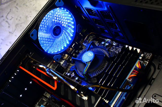 With the increase in computational and texture performance, compared to Hawaii , other performance parameters have not changed much. For example, the number of geometry engines, as well as the theoretical geometry processing speed, remained the same (a little more due to the increased frequency of the video chip in the Radeon R9Fury X versus Radeon R9 290X). But the GCN 1.2 architecture has also seen improvements to speed up geometry processing, and Fiji should be faster than Hawaii in this regard, even at equal peak performance. We will definitely check this in our synthetic tests.
Although the GPU itself has changed very little architecturally, there are several changes associated with the use of a new type of memory. The Fiji GPU includes eight HBM memory controllers, each serving half of the HBM stack (for a total of four on the chip), and each controller is associated with its eight ROPs and a 256 KB L2 cache partition.
Fury X got 60% more video memory bandwidth than the R9 290X (4096-bit bus at 512 GB/s vs. 512-bit bus at 320 GB/s). Together with improvements in frame buffer color information compression, this gives twice the effective bandwidth — and this indicator is one of the key indicators for modern GPUs in real applications. Of course, compression will work well in 3D rendering, but hardly in computational tasks, but in any case, the use of HBM memory gives a good increase in memory bandwidth. But even with such a high bandwidth, the cache is still many times faster, and therefore the size of the L2 cache was also increased in the new GPU: Fiji has 2 MB of L2 cache, compared to 1 MB for the previous top solution.
Important changes have taken place in terms of video data processing — the corresponding Unified Video Decoder (UVD) block has the same capabilities as the Carrizo family APUs and can hardware-accelerate video data decoding in H.265 (HEVC) format. In terms of video encoding, the capabilities of the VCE unit in Fiji have not changed, it can still encode visuals in H. 264 format, but the video decoding unit has received full hardware support for decoding video data in H.265 format, becoming the first discrete GPU with such support. .
AMD also notes the improved scaler and Eyefinity technology — the ability to output images to six image output devices. Unfortunately, the HDMI 2.0 support expected by many is missing from the new GPU. And this is a rather significant drawback, because the most affordable devices with 4K resolution are TVs, which most often have HDMI 2.0 ports and no DisplayPort. Recall that competing Nvidia graphics cards received support for HDMI 2.0 in all GPUs of the second generation of the Maxwell architecture.
Among the advantages of Fiji, it remains to note the support for TrueAudio technology, which the Fiji chip also has. Introduced in the GCN 1.1 family of GPUs, this technology offers hardware-accelerated audio processing on several Tensilica DSPs similar to those included in the main chip of the Sony PlayStation 4 console. Despite all the delights of hardware audio processing in the form of offloading the main CPU from these tasks, TrueAudio support in games is limited to a few games released under the auspices of a special AMD technical and marketing program, and the likelihood of seeing it in other games is not very high.
Design Features and Cooling System
It’s no surprise that AMD chose to build the Radeon R9 Fury X to the same high standards for its elite Fury series as Nvidia did for the Titan. The case of the video card is made of several parts assembled around the printed circuit board, and aluminum alloys with different surface treatments are used in its manufacture, as a result, it looks and feels solid, as required from a top-end solution.
Radeon R9 board bezelFury X, which covers the components on the board, is removable. It is fixed with four screws and can be replaced with a panel made of a different material and with its own pattern — to give the card a personalized look.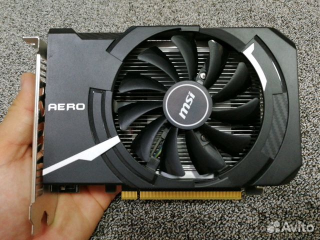 In the case of a video card, which is usually placed inside the case so that its front surface is not visible, this is not so important, but in general, the idea is original and interesting.
For a greater visual effect, we decided to place several LEDs on the board, as well as a red luminous logo — similar to the dual-chip model of the previous generation Radeon R9295X2, the novelty has a red luminous inscription RADEON on the board. Also, the new top-end video card from AMD contains several LEDs that signal the GPU operating mode and are located above the PCI Express additional power connectors.
A bar of eight GPU Tach LEDs indicates the intensity of the GPU work load at the moment. That is, in game mode, all eight LEDs will be lit, and in desktop mode, only one of them is lit. The color of these LEDs is user selectable from red or blue using a switch on the back of the board. And another green LED, located next to them, indicates the activity of the AMD ZeroCore low power mode.
To keep AMD’s most powerful GPU cool, we decided to use a water cooling system that keeps the GPU running under a typical gaming load at around 50 degrees. Water cooling systems have long been the norm in enthusiast systems, and the Radeon R9 295X2 is the first graphics card to feature this type of reference cooler, with closed loop water cooling.
Since the new GPU is very demanding on power and generates a lot of heat, it is no wonder that the Radeon R9Fury X was chosen by a similar system manufactured by Cooler Master. The cooler has a 120 mm heatsink and fan, and their combined thickness is 60 mm, which is quite a lot. As a result, the CBO can easily handle up to 500 watts of heat, far exceeding the Fury X’s typical power consumption figure of 275 watts — a very large headroom.
Although we have already seen more than one video card with water cooling systems, but it was the combination of it with HBM memory that made it possible to significantly reduce the physical dimensions of the printed circuit board and the video card case. The new memory also reduces the number of components in the board’s power system. Therefore, the new product is very different from the usual top-end air-cooled video cards that occupy a couple of slots along the entire length. Radeon R9 PCB LengthThe Fury X measures just 7.5 inches (around 190mm), which is way smaller than typical reference cards in the upper price range.
All components on the board (GPU, VRM and memory chips) are cooled by a single system, equipped with a 120mm radiator and a high-quality fan of the appropriate size from Nidec. The cooler cools the GPU itself and related components, including the MOSFET in the voltage regulator module (VRM) — a special tube is laid for this. The video chip itself with HBM chips placed on it is cooled by the main pump unit.
The cooler used is capable of dissipating up to 500 W of heat, although the model is powered by a pair of 8-pin PCI-E connectors that can transfer up to 375 W, and the six-phase VRM voltage regulator module is capable of providing circuits with a current of up to 400 A — here you can see a large headroom for overclocking enthusiasts, as AMD’s typical Fury X power draw is much lower at just 275W.
Since the cooling system of the Radeon R9 Fury X uses a high-quality large-sized fan, the cooler achieves a fairly low noise level of 32 dBA, which is significantly less than air cooling with a typical 40-45 dBA. Although the first users of Fury X video cards complained about the noise coming from the pump, not the fan, AMD promised to solve this problem in the next batches of boards produced for the market.
Most enthusiasts who buy such video cards are interested in overclocking, including extreme overclocking. And AMD has made some of the task easier by equipping its top-end single-chip card with a powerful cooler and a generous power supply system. Most often, overclocking is limited by lack of cooling or power, and the Radeon R9 Fury X has been designed to minimize these limitations, which should please overclockers.
Using the AMD Overdrive page in the AMD Catalyst Control Center, the user is given the option to set clock speeds, target temperatures, fan speeds, and power limits to control the speed of the graphics card. So far, not everything is clear with the overclocking of the video memory of the new HBM standard, but its overclocking from 500 to 600 MHz gives a noticeable acceleration in games:
I must say that at the time of the release of the card, its overclocking capabilities were seriously limited, AMD did not give the opportunity to increase the voltage and overclock the HBM memory, you can only increase the GPU frequency and the limit of the total power consumption, but there is a very serious backlog. The Dual BIOS switch will also help with this, as in the top-end cards of the previous generation, which allows you to choose between a fixed reference BIOS image and a modified one.
The new High Bandwidth Memory 9 standard0013
As we already mentioned, the main innovation of the AMD Radeon R9 Fury X video card is the use of a new standard video memory — High Bandwidth Memory (HBM). So far, only GDDR5 memory has been used in video cards, which is an evolutionary development of well-known standards, and although it has improved performance and power consumption compared to GDDR3/GDDR4, these improvements are not so significant.
The foundations of the old DRAM standards are many years old, and modifications have resulted in bandwidth gains far short of what GPU performance has grown over time. In twenty years, improvements in standards have allowed memory bandwidth (BW) to rise by only about 50 times, while GPU computing speed has grown much more during this time. Therefore, the industry needed new types of memory that would provide completely different possibilities.
In the GDDR5 standard, this type of memory has reached its limit, and although there are still small opportunities for increasing the memory bandwidth, they require a lot of effort and will not change the situation drastically. At the same time, the issue of high consumption will not be resolved, but energy efficiency is the main parameter for any modern chip. Already current generations of GDDR5 memory consume too much power due to complex clocking mechanisms and operation at a very high frequency, and any improvements in GDDR5 performance are associated with a further increase in frequency and complexity, and therefore power consumption.
Also, GDDR5 chips take up too much space on the board and require the use of multiple memory channels, which complicates the GPU itself. Especially if we talk about top GPUs with 384-bit or even 512-bit memory bus. Although the size of video cards in itself does not matter too much for gaming PCs, but recently there have been many compact cases in new form factors that current video cards cannot be used in.
To solve all these problems, back in 2011, AMD and Hynix announced joint plans to develop and implement a new memory standard — High Bandwidth Memory. The new type of memory was a huge step forward compared to the GDDR5 memory used so far, and among the main advantages of HBM are a significant increase in bandwidth and increase in energy efficiency (reduction in consumption along with an increase in performance).
Recall that AMD, like ATI in previous years, has recently been a leader in the development of new types of graphic memory. Although they were not the first to release products with support for GDDR2 and GDDR3, it was this company that was the first to equip its solutions with video memory of the last two existing standards: GDDR4 and GDDR5. Accordingly, in 2011, in partnership with Hynix, they decided to continue the initiative to prioritize the development and implementation of new video memory standards in future GPUs. And now, after four years of development, the companies have finally introduced a GPU equipped with a completely new type of graphics memory.
The HBM standard differs in that instead of an array of very fast memory chips (7 GHz and higher) connected to the GPU via a relatively narrow bus from 128 to 512 bits, very slow memory chips (of the order of 1 GHz effective frequency) are used, but the width the memory bus in this case is several times wider. As in the case of GDDR5, the bus width for different GPUs will be different and it depends both on the generation of the HBM standard (the first or second at the moment) and the specific implementation.
The Radeon R9 Fury X uses four stacks (stacks, stacks or packs) of memory chips, each consisting of four chips and giving a 1024-bit memory interface.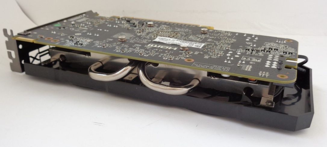 That is, as a result, on the GPU, a 4096-bit bus is obtained that is wide by the standards of GDDR5 memory. Naturally, in this case, memory chips do not have to operate at the same high frequencies as in the case of GDDR5 — a relatively low frequency will be enough to bypass the usual interfaces in terms of memory bandwidth (PSP).
A 4096-bit memory bus requires significantly more connections than conventional GDDR5, and all of them must physically fit in order for such a bus to work. It is these parallel connections that are the main problem in connecting the GPU to HBM memory, and several new technologies are used to successfully solve the problems of locating them in a new type of memory.
The most important issue is the efficient layout of the 4096-bit memory bus. After all, even the latest chip manufacturing technologies have their limits, and GPUs have never crossed the 512-bit limit, even in the latest top-end graphics chips like Hawaii. It is theoretically possible to organize an even wider memory bus on large GPUs, but solving this complex problem will limit the physical possibilities for placing such a number of connections both on a printed circuit board and in the chip itself, not to mention the required number of contacts on BGA-type packages.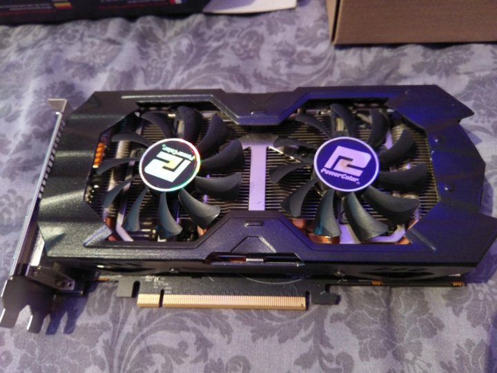
The solution to this problem was the development of a special layer that can accommodate high-density compounds — a silicon substrate (interposer). This layer is similar to an ordinary silicon crystal, in which, instead of some internal logic, metal layers are placed to transmit signals and power between various components — a kind of adapter is obtained. The interposer is manufactured using the capabilities of modern lithographic processes, which allow the placement of very thin conductors that are almost impossible to fit on traditional printed circuit boards.
The use of an adapter layer solves some of the fundamental problems of accommodating a wide memory bus, and also provides other advantages. So, along with solving the problem of routing conductors, this silicon substrate allows you to place memory chips very close to the GPU, but not directly on the chip, as is used in the cases of some mobile systems-on-a-chip. And if you place the memory chips close to the graphics chip, then long connections between them are not required, which simplifies the design and imposes less stringent power requirements.
Putting the memory chips together with the main logic also benefits in increased integration — more functional logic can be assembled in one package, which reduces the amount of external wiring required. As a result, AMD released the first mass-produced product using the interposer layer, and became the first company to release a solution using stacked DRAM and integrating HBM and GPU chips.
Of course, the solution with an intermediate layer has its drawbacks — the complexity of the design and the increase in production costs. Naturally, no one from AMD talks about the production cost of the first chips with HBM, but it is obvious that adding an additional layer, as well as connecting it and testing the entire product, which includes the most complex logic, can only increase its cost, especially at the very beginning of its production. And especially — compared to the long-established technologies for the production of traditional printed circuit boards and chips without a bunch of layers connected to each other.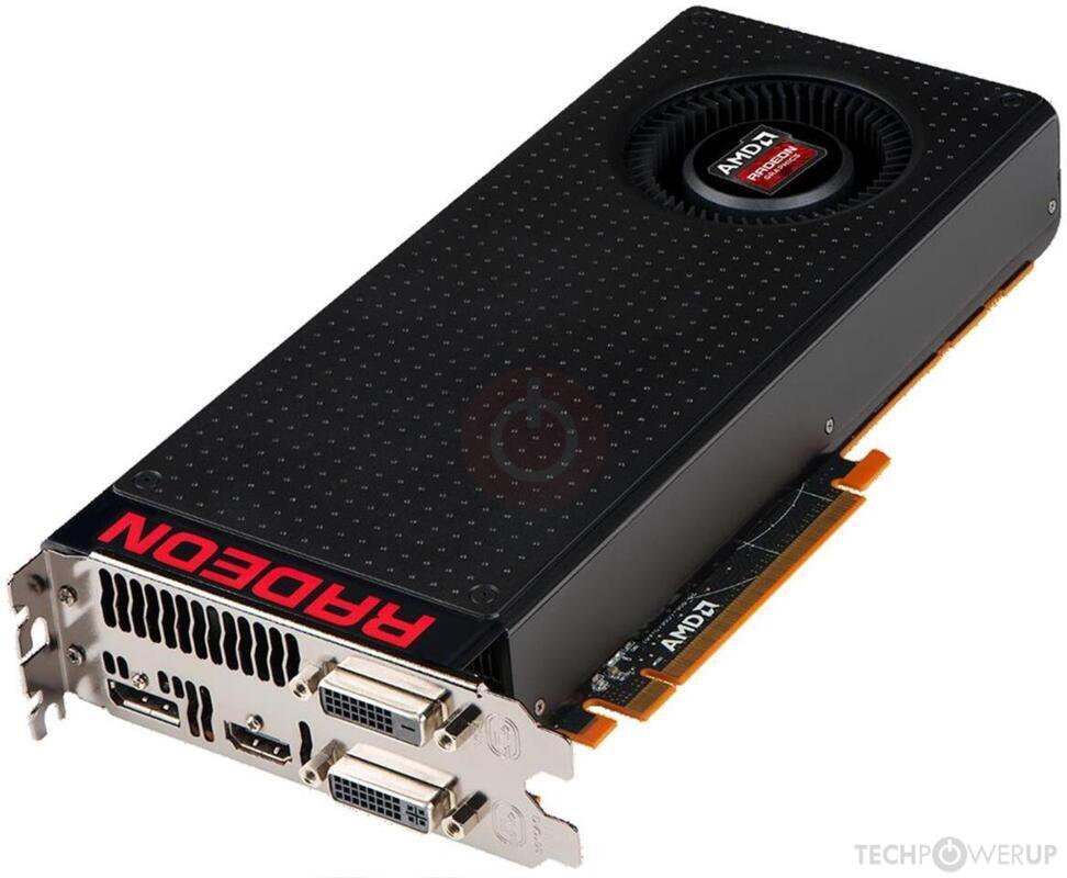
Looking at the whole «sandwich» in the section, you can see that the interposer becomes a new layer between traditional packaging and DRAM chips with additional control logic mounted directly on the interposer. To connect the memory chips and logic with the interposer, special connections such as microbump and TSV (through-silicon vias) are used, then the interposer is connected to the main crystal, which is already habitually connected to the printed circuit board with BGA contacts.
The connection of the HBM memory chip to the printed circuit board is somewhat simplified, since in this case there will be no connecting lines to the memory chips on the PCB, only lines for data transmission remain (via the PCI Express bus, etc.) , as well as to power the graphics processor and memory chips. Some of these complexities go to the interposer layer, so testing it during production becomes one of the most important tasks.
Another important technological point in connecting HBM memory chips to each other is to create through-silicon vias (TSV) connections.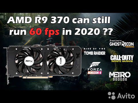 Conventional junction types allow you to connect two layers together, and TSV extends this by connecting further silicon layers. From a manufacturing point of view, TSV-type connections are more difficult to manufacture and stacking DRAM chips is a technological challenge. Attached to the stack of memory chips at the bottom is a logical core, which is responsible for the operation of all DRAM chips in the stack and manages the HBM bus between the stack and the GPU.
The main limiter for further performance growth now is the ability to manufacture an interposer layer — it needs to make a lot of very small connections for several memory layers. That is why the number of layers is currently limited to four, and the placement of eight layers will have to wait a bit — the second generation HBM will already have eight layers (and twice as much memory bandwidth, all other things being equal, respectively). Otherwise, HBM2 will not differ much from HBM1, except that ECC error correction is still expected, which is important for use in professional solutions.
But the second generation will not appear until next year, but what does the use of HBM in the Radeon R9 Fury X give? The first generation of HBM, which powers AMD’s new top-end GPU, allows for 1024-bit, four-chip stacks running at up to 500 MHz, which is equivalent to 1 GHz effective DDR memory. That is, each stack is capable of providing up to 128 GB/s of video memory bandwidth. This gives us a total throughput of 512 GB/s.
Of course, this is noticeably more than 320 GB / s for the Radeon R9290X and 336 GB / s in the best card of the competitor GeForce GTX Titan X, but provides only up to 60% increase in memory bandwidth — not too much for a completely new type of memory with such a wide bus, because purely theoretically one can assume the appearance of a GPU with a 512-bit bus and the use of a very fast GDDR5 memory, which in terms of bandwidth is not inferior to the first version of the HBM memory. AMD representatives also claim that memory access latencies in the case of HBM are slightly lower — by 15-20% compared to GDDR5. This is not so important for graphics tasks, but it is very important for CPU and some GPU computing tasks.
But, in addition to increasing the bandwidth and a slight decrease in delays, the use of HBM also reduces the energy consumption of the entire memory subsystem. In the current top-end Radeon R9 290X solution, up to 15-20% of 250 W of total power consumption is spent on powering GDDR5 chips — that is, up to 37.5-50 W in absolute terms. According to other AMD data, it follows that GDDR5 provides 10.66 GB / s of memory at 1 W, and the consumption of GDDR5 memory is slightly lower — 30 W. HBM memory provides more than 35 GB / s per watt, that is, it provides more than three times better energy efficiency compared to GDDR5.
The energy efficiency advantage improves performance and/or saves energy. The latter is important for mobile solutions, and for a top-end GPU, you can increase its power in the absence of an increase in energy consumption. If we take the value of the final memory bandwidth of 512 GB / s with four stacks of HBM memory, then such chips will consume about 15 W versus 30 W for 320 GB / s GDDR5 in the case of the Radeon R9 290X. A difference of 15 or even 20-25 watts (with the difference in memory bandwidth) can be spent on increasing the performance of the GPU itself, because PowerTune power management technology limits the overall consumption of the video card, and a large share of the power allocated to the GPU allows AMD to increase clock speeds and voltage for the top GPU using HBM.
A sharp increase in memory bandwidth will be useful in any case, and the use of HBM will only improve the overall performance. But there is one caveat here — even with an advantage in memory bandwidth, AMD’s previous solutions were either no faster than rival Nvidia video cards, or even somewhat slower than them. But since AMD’s new GPU is based on the GCN 1.2 architecture, the situation has noticeably improved, since it was in this version of the architecture that new frame buffer data compression methods were introduced, correcting the situation with the insufficient efficiency of using the available memory bandwidth. And the new top-end AMD graphics processor received not only a high memory bandwidth, but also improved efficiency of its use, which is especially important at high resolutions.
Another advantage of HBM memory, noted by AMD in their materials, is the compact physical size of the entire device — the GPU, along with DRAM chips, takes up very little space, compared to our usual form factors with a large printed circuit board, a separate GPU and memory chips placed on it at some distance. Replacing GDDR5 memory chips with small HBM stacks reduces the size of the entire video card.
Thus, each gigabyte of GDDR5 memory, consisting of four two-gigabit chips, takes up to 672 mm 2 , and the same amount of HBM memory in the form of an HBM stack will take only 35 mm 2 — almost 20 times less! Even if we recalculate the figures using 4-gigabit microcircuits, the difference in the occupied area will remain almost an order of magnitude.
Even if we take the area occupied by all microcircuits on the PCB, it turns out that the packaging of a GPU with HBM memory will take about 4900 mm 2 versus 9900 mm 2 for the previous generation Radeon R9 290X video card.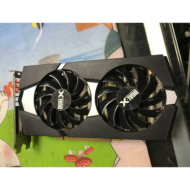 Additional space savings can be used for various purposes, especially since HBM memory stacks do not need a separate complex power subsystem — the difference in practice will be even greater.
Everything seems to be great, but there are some questions about the provision of cooling, since in the case of such a solution, the DRAM chips and the GPU itself will be in one package, which is covered with a single heat-removing cover that covers both the HBM stacks and the GPU core. Is sufficient cooling provided for the entire system in this case, and how will the operation of the memory chips be affected by the proximity to an extremely hot GPU core?
Well, the main alleged disadvantage of the proposed configuration of four stacks of HBM memory may be the total amount of video memory — after all, four stacks of 1 GB each give only 4 GB in general. Equipping the new top AMD product with only 4 GB of memory, albeit very fast, can potentially become problematic, because the competitor’s solutions have more video memory, albeit slow GDDR5.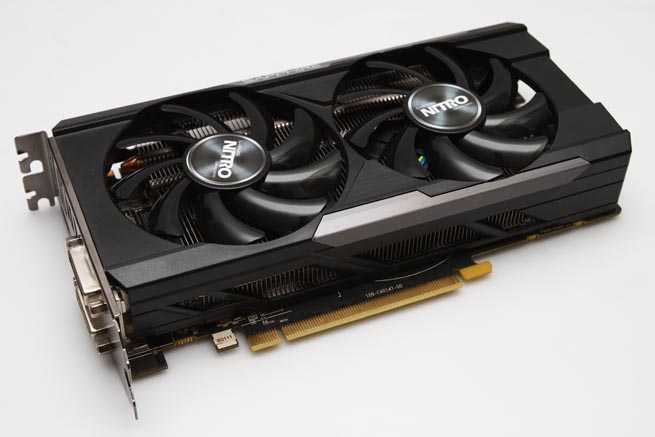 Apparently, the current design allows only four stacks around the GPU, which limits the total amount to four gigabytes.
True, 4 GB of video memory is still very often used even in top-end solutions, and so far it is quite enough in most games with any settings. But the latest games like GTA V and Call of Duty: Black Ops 3 can often use more video memory, especially at the highest resolutions like 4K. And if there is not enough video memory for buffers, game textures will be loaded into memory, then free it, which will cause performance degradation and uneven frame rates. But now it is 4K and VR that are the main engines of the industry, and all of them only increase the requirements for video memory, as well as multi-monitor configurations, which AMD solutions are famous for supporting.
It turns out that even for a gaming solution, having only 4 GB of HBM memory can be controversial, not to mention professional use. Although situations with a shortage of this amount of video memory are very rare so far, a top-end video card with such a price should have some margin of safety so as not to become obsolete in the next couple of years. And with 8GB of shared memory available on current-gen major gaming consoles, 4GB of VRAM may soon be out of reach for more games.
Perhaps AMD decided to use such memory a little early, and it was necessary to wait for the commercial availability of the second generation of HBM memory, because its main difference is that the number of DRAM chips per stack will be doubled, which means the volume will increase to 2 GB per stack , which will allow the release of a graphics chip with 8 GB of video memory. But this will be possible only next year, and the second generation will be available not only for AMD, but they clearly wanted to be the first to master the new memory.
Not only was AMD the first GPU manufacturer to use HBM memory, but also the only manufacturer to master first-generation HBM memory. After all, only the second generation, HBM2, will become the standard approved by the JEDEC committee, and the first generation HBM will be used exclusively jointly by AMD and Hynix.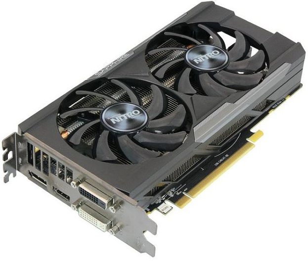 And before the appearance of products using the second generation of HBM, AMD has about a year of head start in applying this technology. It is quite possible that they will also master the second generation of HBM2 faster than their competitor — after all, they already have quite a lot of experience in working with HBM stacks.
Software technologies
Let’s talk about the software technologies that have been improved and introduced with the release of the Radeon R9 Fury X. We wrote about some of them back in December last year, when the drivers codenamed Omega were released, it was they who introduced support for Virtual Super resolution Resolution — rendering in a higher resolution and then reducing the image to a lower resolution of the output device.
Although this was a response to the competitor’s similar DSR technology, they differ markedly from each other in their approach. Nvidia uses a special shader to change the resolution, which gives a more flexible approach that allows you to change the filtering quality, but with some performance drop.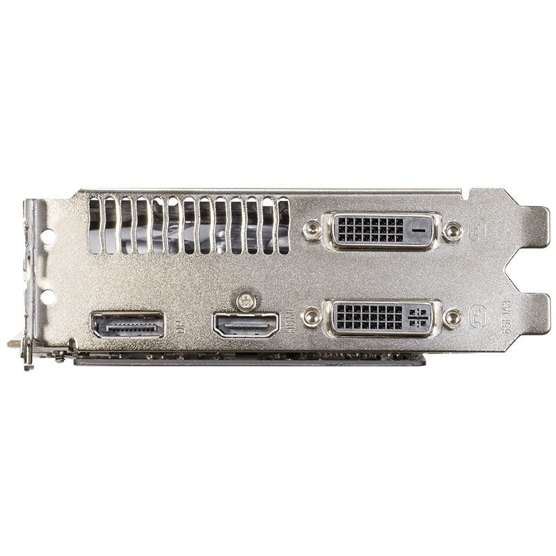 AMD’s VSR technology, on the other hand, works directly through the display controllers, so it does not lead to a drop in performance, but does not provide such flexible options for filtering and adjusting picture quality as DSR.
Because VSR is limited by the display controllers used, it is the latest generation of AMD GPUs that are better able to use virtual resolutions. So, controllers of the previous generation (GCN 1.1 families) cannot work in 4K resolution, and the same Radeon R9 290X is limited to a maximum virtual resolution of 3200 × 1800 pixels, but GCN 1.2 chips (Tonga and Fiji) support resolution reduction from 4K resolution , which will be in demand in the Radeon R9Fury X, since the Radeon R9 285 is too weak for such tricks.
Radeon R9 Fury X and 1080p monitors support 3200×1800 and 3840×2160 pixels, 2560×1600 and 3840×2400 for 1200p monitors, and only 3200×1800 for 1440p. So the lack of flexibility of VSR is clearly visible here, compared to DSR, which allows you to change the virtual resolution in a much wider range.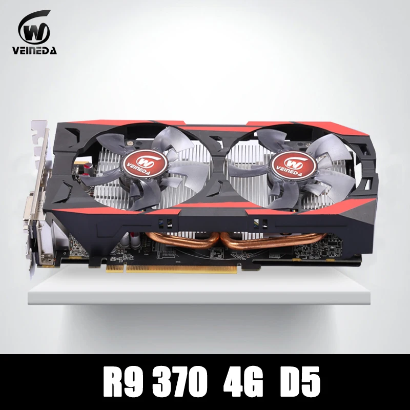 Well, at least there is an analogue of 2 × 2 supersampling (albeit with a straight pixel grid), in the form of a virtual 4K resolution for FullHD monitors — one of the highest quality options.
Among the new software technologies, one can note the possibility of limiting the frame rate during rendering — Frame Rate Targeting Control (FRTC). This new feature was introduced in the latest AMD drivers and allows the user to set the maximum frame rate for 3D applications running in full screen mode. Although utilities like MSI Afterburner have been offering this functionality for a long time, official support in AMD drivers will be more convenient for most users.
As a result of the FPS limit, the board will operate at a reduced load, reducing power consumption, heat generation, and noise from the cooling system. With the FPS limit set in games that are not too demanding, the GPU will consume less power, as it will be idle part of the time, which will also cause a decrease in power consumption with heat dissipation — and this, in turn, will reduce the noise from the cooling system.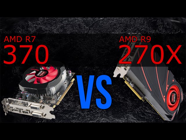 The diagram shows real examples from a couple of games:
Moreover, FRTC works not only for 3D scenes, but also in the case of game splash screens, loading screens and menus, when FPS is often hundreds of frames per second. With the help of the FPS limiter, you can set a high enough frame rate limit so as not to lose in the «responsiveness» of the game, but reduce FPS in the case of splash screens and menus, when resources are spent senselessly.
In its current form, Frame Rate Targeting Control only works in DirectX 10 and DirectX 11 applications, and the maximum frame rate can be set between 55 and 95 fps. AMD is currently advertising FRTC support only for its new series of video cards, so it is not yet known for sure whether it will be enabled for solutions of the previous generation Radeon 200, although they are based on exactly the same chips as the Radeon 300.
In their materials, the company AMD is also careful to mention Microsoft’s graphics API support for the new version, DirectX 12.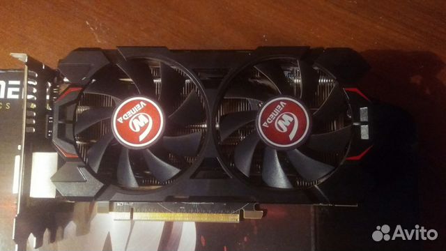 This is the latest version of the well-known graphics API, the details of which are similar to what was done in the «console» graphics API some time ago — providing direct control over resources GPU. This approach allows you to better exploit the full capabilities of the CPU, GPU and hybrid chips like APU, and, ultimately, improve the performance of 3D applications and / or improve image quality.
The new AMD Radeon family of graphics cards fully support all of the new features of Microsoft DirectX 12 — which are included in the so-called Feature Level 12.0 feature level, including tile resources that are used to apply dynamically loaded virtual textures in large 3D scenes with unique surfaces. And the API itself in the new incarnation has become simpler and clearer, plus, in this version of DirectX, a multi-threaded instruction buffer recording has appeared, which makes it possible to better use the capabilities of multi-core CPUs.
Recall that in DirectX 11, the performance of 3D rendering with a large number of drawing function calls is often limited by the computational speed of a single CPU core.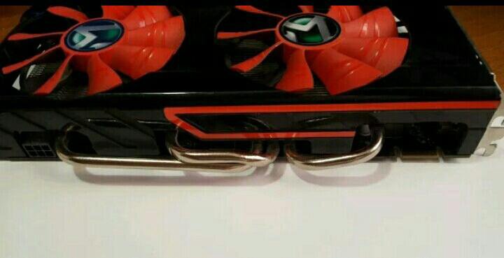 In the case of DirectX 12, the work is parallelized across several CPU cores, and in general, the rendering speed is limited by the capabilities of the GPU, and practically does not rest on the capabilities of the CPU. As a result, it becomes possible to use more draw calls, getting more detail in the scene and objects. Well, the freed CPU resources can be used by the game code (AI, etc.).
With DirectX 12, all the work of the game engine and graphics API can be much better distributed across all available cores, allowing for more complex 3D scenes. As for the performance of the new graphics API, compared to the previous version, it can be evaluated in a special 3DMark API Overhead feature test that measures the effectiveness of the API with a large number of draw function calls:
As you can see, when using DirectX 12 and Windows 10, the new AMD’s top graphics card provides a huge increase in the number of draw calls per second compared to DirectX 11 and Windows 8.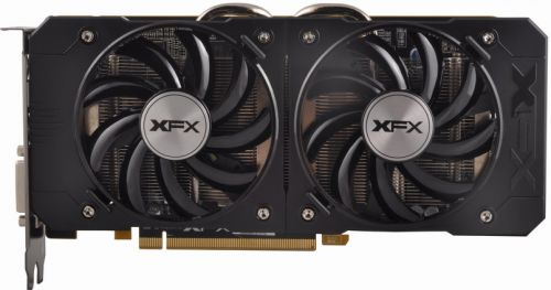 1, and is also almost one and a half times faster than the competitor’s solution in DirectX 12 mode.
Among the changes in DirectX 12, one can also mention the asynchronous execution of shaders, when complex tasks are divided into several simple ones that are executed in parallel. In the previous version of DirectX 11, shadow rendering, lighting rendering, data read/write, and non-graphics calculations are performed sequentially, often using different GPU resources, and the rest are idle. Tasks could be executed in parallel, which was supported in DirectX 12. This allows for better use of GPU resources, increased performance and detail, and more complex visual effects.
By the way, the modern Graphics Core Next graphics architecture includes special Asynchronous Compute Engines (ACEs) that help to perform the work of asynchronous shader execution at maximum speed, so AMD graphics solutions should cope with the new API perfectly.
Appeared in DirectX 12 and native support for multi-chip configurations consisting of several GPUs. Previous versions of the API did not provide for the existence of such configurations consisting of several GPUs, and developers had to deal with the distribution of work between GPUs in drivers and games on their own. But the lack of hardware management, limited combinations of multiple GPUs, and the difficulty of distributing work across multiple GPUs resulted in under-optimized performance for such systems.
And DirectX 12 introduced developer resource usage controls to better distribute work between GPUs, as well as standard support for APU and GPU configurations so developers can give some of their work to the APU. The appearance of support for several video cards in DirectX 12 allows you to get better performance from multi-chip systems and effectively use configurations that simply could not be used earlier in DirectX 11.
known and used by multi-chip video systems) rendering method — SFR (split-frame rendering). This method differs in that the frame during rendering is divided into several areas (tiles), which are rendered by different GPUs. The result is that all available GPUs work on each frame as if one more powerful chip, which leads to lower delays in displaying the image, although it does not provide such an effective frame rate doubling as in the usual Alternate Frame Rendering (AFR), known from existing CrossFire and SLI video systems.
Among the games that will benefit from some of the features of the new API version, AMD highlights a couple of games coming out with support: Deus Ex: Mankind Divided and Ashes of the Singularity.
Brief Theoretical Performance Evaluation
To make a preliminary assessment of the performance of AMD’s new top solution, let’s take a look at some numbers and the company’s own test results. With 4096 streaming cores and the fastest High Bandwidth Memory on board, the Radeon R9Fury X is clearly aiming at the highest price range of gaming graphics cards. With unrivaled math performance and memory bandwidth, AMD’s newest product offers the best performance in its class.
Although the peak speeds of the ROPs and geometry blocks barely increased, both types of execution units should perform noticeably more efficiently in the case of Fiji. Based on the theory, the Radeon R9 Fury X should be noticeably faster than the Radeon R9290X and R9 390X, based on the Hawaii GPU, but the difference in speed will depend on the type of workload — more emphasis on computing, texturing, geometric calculations or fill rate.
In the case of pure computing workloads, a 45% increase in the number of ALUs and a 5% increase in clock speed give Fury X more than 50% advantage over the R9 290X (and R9 390X). In the case of emphasis on the performance of ROP blocks, the difference can be as much as 5% if the data in the frame buffer is poorly compressed and there is no emphasis on the memory bandwidth, or more than 100% if the new compression algorithms work as efficiently as possible. On average, you can expect about a third of the increase in speed compared to the flagship of the previous AMD line, but at high resolutions, the new Radeon R9 modelFury X should show even more power.
Since the new top-of-the-line Radeon R9 Fury X graphics card is designed for enthusiasts and has very high performance, it is not surprising that AMD compares the new card in speed with a competitor in the highest resolution — 4K (3840 × 2160 pixels). First, let’s look at the 3D rendering speed of the Radeon R9 Fury X and GeForce GTX 980 Ti in 3DMark Fire Strike Ultra, which traditionally favors the GCN architecture:
As you can see in the diagram, the advantage of the new top-end AMD graphics card is there, albeit a small one. But it was a synthetic test, but what happens in real gaming applications? On the following chart Radeon R9Fury X takes on the same rival GeForce GTX 980 Ti, rendering in 4K resolution at maximum quality in the most popular games.
Well, at least according to AMD’s measurements, it turns out that the Radeon R9 Fury X turned out to be on average a little faster than its competitor in games and 4K resolution, and what happened to us — see our review.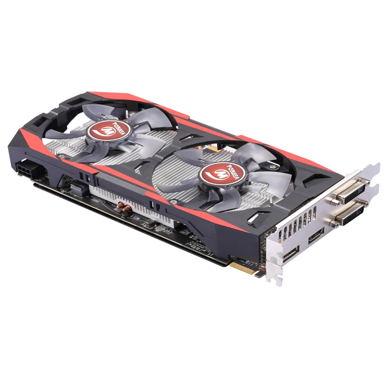
Summary
With the recently announced Radeon R9 Fury X, AMD offers a very interesting top-end graphics card. Most importantly, they were able to provide a full-fledged product from the upper price range, while the previous single-chip top-end solution in the form of the Radeon R9290X clearly lost to a competitor. With the release of Fury X, the company decided to move into the segment of elite solutions, which are distinguished not only by the highest performance and complexity, but also by an increased price. Based on the most sophisticated Fiji GPU, the first video card of the elite Fury sub-series turned out to be very interesting in many respects.
The novelty is interesting both from the market and technical points of view. Technically, AMD has done a lot of interesting things, suffice it to mention even the world’s first use of the latest type of HBM memory, which not only significantly increases memory bandwidth and reduces power consumption, but also provides new opportunities for miniaturizing the form factor of future video cards.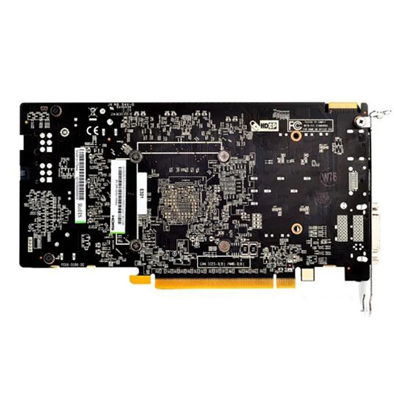 But not only the GPU with HBM turned out to be interesting in itself, the quality of materials and assembly of the video card is also excellent, and the power supply and water cooling systems are very efficient and have a huge margin of safety.
In Fury X, the company’s engineers have done everything possible within the GCN architecture to successfully compete with Nvidia’s top solutions based on Maxwell chips, including even the elite GeForce GTX Titan X solution — if the Californian company had not released the GeForce GTX 980 Ti, then in battle AMD’s solution would definitely win the tops — but not in terms of absolute performance, but in terms of the ratio of price and speed of video cards. Unfortunately for AMD, the competitor released the GTX 980 Ti a little earlier at exactly the same price, and the new product will have a long market struggle with this solution.
At high resolutions like 4K, and with enough 4GB of VRAM, the Fury X can conceivably be slightly faster than its rival due to its higher memory bandwidth, but the difference between the two should not be too big in any conditions. At lower resolutions, while reducing the influence of the memory bandwidth of a very fast HBM memory and focusing on the performance of other GPU or CPU units, the new top-end solution from AMD may already be somewhat slower than the GTX 980 Ti. Alas, this is not enough for a clear victory, especially since modern games in 4K resolution are starting to hit the memory limit of 4 GB, not providing a sufficiently high frame rate.
In our opinion, the only important potential disadvantage of the Radeon R9 Fury X is the strictly limited amount of HBM type video memory. At the moment, it simply cannot be installed anymore, because the first generation of HBM essentially limits the total volume to this value. However, at the moment, 4 GB is enough in 99% of cases, only rare games like Grand Theft Auto V, Call of Duty: Black Ops 3 or Far Cry 4 at maximum settings start to suffer from a lack of memory for streaming textures. But top video cards are bought not for half a year, but for a year and a half or two, there can be much more examples of such games, and this is alarming.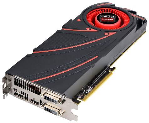
When comparing two direct competitors, the clear advantages of the GeForce GTX 980 Ti include more video memory and lower overall power consumption. But the Radeon R9 Fury X also has its advantages: huge computing performance, the highest memory bandwidth, a small physical size of the board, as well as a very efficient and quiet (minus the noise from the pump in the first copies) water cooling system. The choice is up to the user, because both boards are very worthy and have their own characteristics. 96) ALU for floating point calculations (integer and floating point formats are supported, with FP32 and FP64 precision)
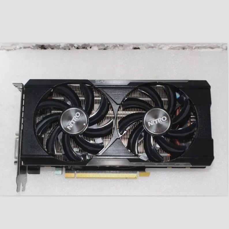 2
2 64.0160033
If the top solution of the premium subfamily, which has a water cooling system on board, was called Fury X (“extreme”), then the usual “air” model was simply called Fury. And the Radeon R9 Fury has taken its position at the top of AMD’s product line, one notch below the Fury X. AMD between two graphics cards from rival Nvidia: GeForce GTX 980 Ti and GTX 980, but closer in positioning to the new product is the younger model GeForce GTX 980 with an official recommended price in the North American market of $499.
It turns out that the announced Radeon R9 Fury is slightly more expensive than its closest competitor, but should provide slightly higher performance than the GeForce GTX 980. several such variants of the GTX 980, which just have a price close to $650.
As we have already mentioned, the most controversial decision in the characteristics of all Fury models is the presence of only 4 GB of video memory, which, although for the time being, is enough even for high resolutions at maximum quality settings, but in a number of modern games at 4K resolution and full-screen anti-aliasing with High quality settings require even more volume.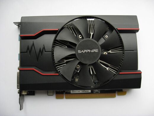 The first generation of HBM memory simply does not allow you to make a board with 8 GB of such memory. However, for the price of $550, such a volume is more or less justified, since the closest competitor in the form of the GeForce GTX 980 with GDDR5 memory has the same amount of video memory.
By itself, the Radeon R9 Fury is no longer as compact as the Fury X, it matches the dimensions of typical high-end air-cooled cards, so the HBM memory itself does not allow for a decrease in the physical size of the video card, even though fewer components on the board, including in the power circuit. The use of a very powerful GPU with HBM chips on it leads to the need for effective cooling with a rather large air cooler, most often with three large fans.
Interestingly, the typical power consumption (Typical Board Power) for the Radeon R9 Fury remained exactly the same as in the case of the Fury X — 275 watts. In theory, Fury should have received some reduction in consumption, since some of the GPU functional blocks in it are disabled, and the rest runs at a slightly reduced frequency.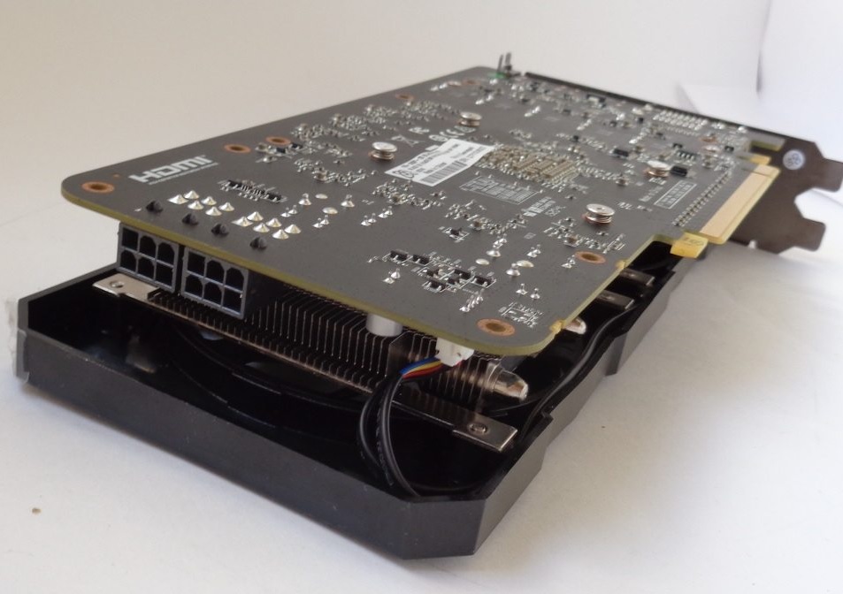 This is probably because video cards with a truncated GPU use chips with worse overclocking characteristics, and even work at higher temperatures, which leads to greater energy losses and poorer energy efficiency in general.
Unlike the Fury X model, which has a reference design that is the same for all manufacturers and is characterized by compact dimensions and a water cooling system, the «simple» Fury does not even have a full reference design. The company’s partners do it themselves, and the printed circuit boards for Fury have a traditional size for top-end video cards and powerful air cooling. This is probably why the reviewers received samples of the Radeon R9 Fury not as quickly as in the case of reference cards, and this model went on sale later than the official announcement.
The first companies that were allowed to release the new product were AMD’s most reputable partners in the form of Sapphire and ASUS. Sapphire released a couple of solutions at once: a model with reference frequencies and a factory overclocked video card based on an AMD PCB and a Tri-X cooler of its own design.
This cooler is equipped with a smart fan speed control system that ensures maximum performance at a target temperature of 75 degrees. An efficient cooling system keeps the noise level below 25 dB at 1200 rpm fans, and at low load on the GPU, when the temperature of the GPU does not exceed 50 degrees, they stop altogether.
ASUS has decided to release a completely custom version of the printed circuit board, providing it with a branded DirectCU III cooler — the ASUS STRIX Radeon R9 Fury model, which also has three efficient fans in the cooling system. Over time, other manufacturers also received the opportunity to release video cards of the Radeon R9 Fury model.
Architectural and functional features
Since the Radeon R9 Fury is based on the same Fiji GPU that we already reviewed in the Radeon R9 reviewFury X, many data can be learned from the relevant material, including: architectural features, a brief overview of the HBM standard memory, new software features that include advanced support for DirectX 12, and much more.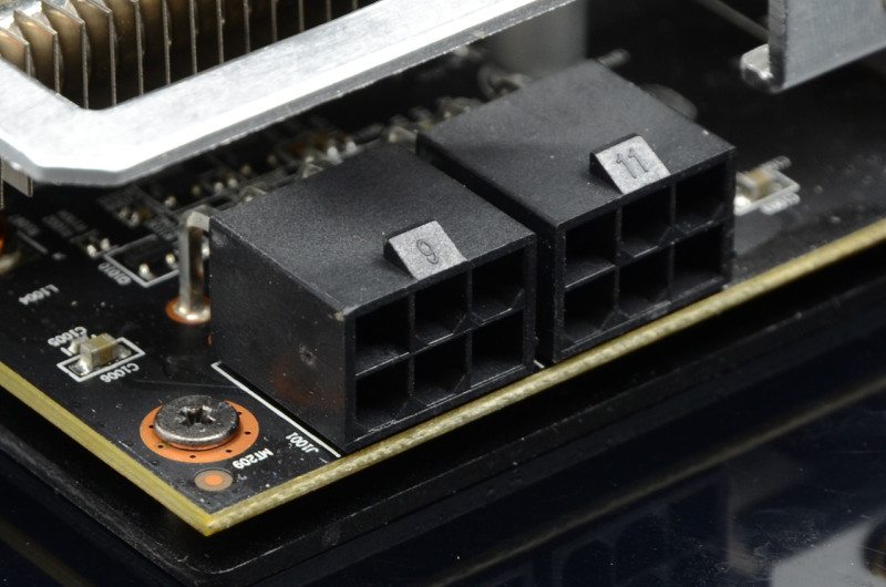 It is also useful to read the material about the long-known Graphics Core Next (GCN) architecture, which underlies all modern AMD solutions.
Although the Fiji GPU has had some changes from last year’s Tonga, it is the third generation of GCN — it can be loosely referred to as version 1.2. The new top-end GPU includes all of the GCN 1.2 enhancements, including improved geometry and tessellation performance, new framebuffer lossless data compression, some 16-bit multimedia instructions, and increased L2 cache to 2 MB. In terms of computing capabilities, the new GPU received improved scheduling and task distribution and several new instructions for parallel processing of data — all this is described in detail in the Radeon R9 review.Fury X.
Schematically, the Fiji GPU is similar to Hawaii, released back in 2013 — both GPUs are divided into four Shader Engines, each of which has its own processor for processing geometric data and a rasterizer, as well as four enlarged ROPs , capable of processing 16 pixels per clock (a total of 64 ROPs in each of these chips).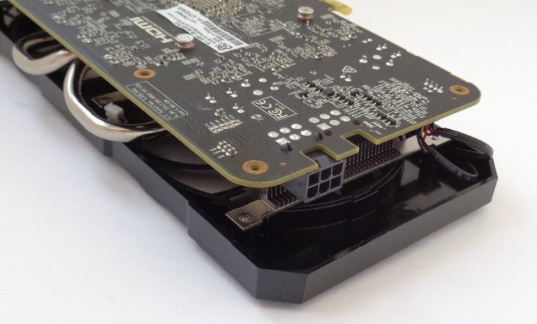 The GPU has a single command processor and eight Asynchronous Compute Engines, which have been modified to reflect the changes in GCN 1.2.
But Fury uses a truncated version of the video chip, and the specifications of the Radeon R9 Fury show how much the Fiji GPU was cut relative to its full-fledged version in Fury X. AMD made a modification typical of slightly less expensive top-end video cards by blocking the hardware part of the execution units, as well as slightly lowering the GPU clock speed — this allows you to use defective processors that were not suitable for the production of Fury X — with partially inoperative stream processors or with slightly worse high-frequency capabilities. Consider the Fiji chip modification scheme for the Radeon R9 modelFury:
The Fiji GPU in the Radeon R9 Fury includes 56 Compute Units (CUs) out of the 64 physically present in the GPU. That is, the total number of stream processors in this model has been reduced from 4096 to 3584. Together with the number of ALUs, the number of texture units has also decreased, since they are part of CU units in the amount of 4 pieces for each.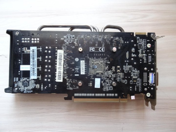 Accordingly, 224 out of 256 physically available TMUs remained in Fury.
Traditionally for AMD solutions, other GPU blocks were not touched, so the number of geometry blocks and ROP blocks was not reduced. As the characteristics of the memory subsystem remained exactly the same, including the amount of cache memory. Both Fiji-based video cards currently released have 4 GB of HBM memory connected directly to the GPU using 4096-bit memory bus. It seems that it is the relatively small amount of video memory for top-end solutions that does not allow lower-end solutions to be cut in terms of HBM characteristics as well — it would be strange to have such an expensive board with less memory.
Naturally, the GPU clock speed was reduced, but in the case of the Radeon R9 Fury model, it decreased insignificantly — only from 1050 to 1000 MHz, that is, only 5% less than that of the top Fury X model. But the video memory frequency not touched, it is still the same 500 (1000) MHz as in the case of Fury X — that is, there is no difference between this pair of models in terms of memory bandwidth.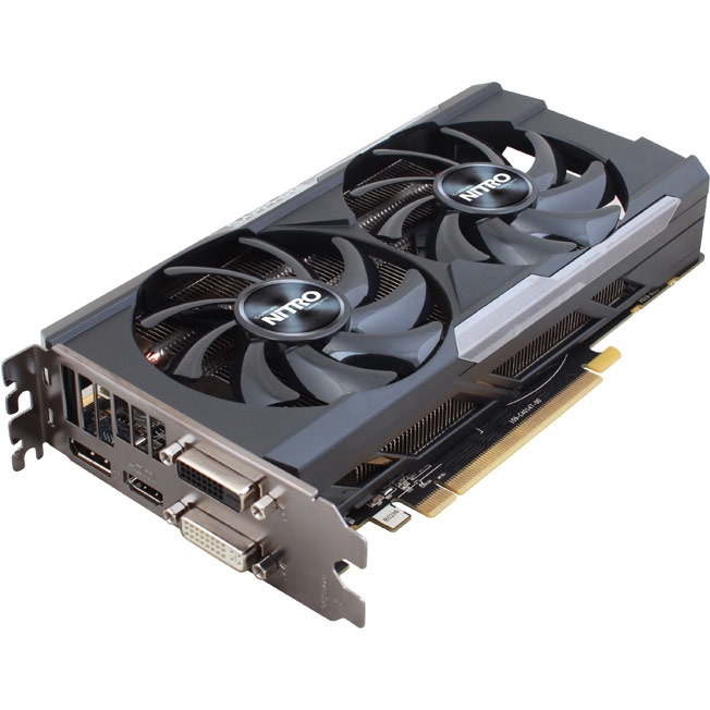
In all other respects, the Fiji chip is exactly the same as in the Fury X, it is equipped with HBM memory, has improved video data processing units, etc. In particular, the Unified Video Decoder decoding unit can hardware accelerate the decoding of H.265 (HEVC) video data, and the Fiji chip became the first discrete GPU with such capabilities. Among other advantages of Fiji, we note support for TrueAudio, LiquidVR, Mantle, Eyefinity and FreeSync technologies, which we have repeatedly written about in our articles.
Theoretical Performance Evaluation and Conclusions
In order to make a brief preliminary evaluation of the performance of the new solution, we will review the theoretical parameters and the company’s own test results. With a large number of streaming cores and the fastest High Bandwidth Memory on board, the Radeon R9 Fury is clearly a typical high-end gaming graphics card designed to play at the highest resolutions at the highest quality settings.
Based on theoretical performance, the performance difference between Fury and Fury X is up to 20% (3584 ALUs running at 1000 MHz are slower than 4096 at 1050 MHz). That is, if rendering performance depends precisely on the speed of the ALU or TMU, then Fury will be slower by about that much. But if performance in a 3D task is limited by memory bandwidth, then Fury will not lag behind Fury X at all, having the same 512 GB / s. Well, if the rendering speed is limited by the possibility of geometric blocks or fillrate (ROP blocks), then the difference in speed should not exceed 5%. In real games, the difference between Fury and Fury X should be somewhere between 7-10% — somewhere between 0% and 20%.
Since the new top-of-the-line graphics card Radeon R9 Fury is designed for enthusiasts and has very high performance, it is not surprising that AMD compares the new card in speed with a competitor in the highest resolution — 4K (3840×2160 pixels). In the following chart from the company, we see a comparison between the Radeon R9 Fury and its main rival, the GeForce GTX 980, in some popular games, when rendering at 4K resolution at maximum quality, but without enabling full-screen anti-aliasing:
The rejection of full-screen anti-aliasing is understandable — in such conditions, the lack of 4 GB of video memory at 4K rendering resolution would become quite noticeable, both for the Radeon R9 Fury and for a competitor.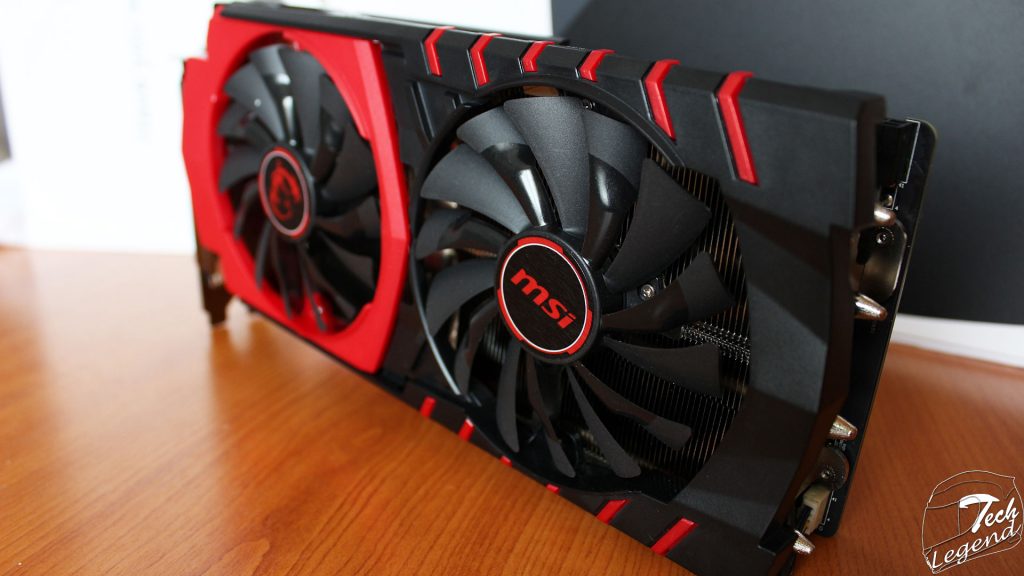 If anti-aliasing is not enabled, then AMD’s new product, according to their own data, turns out to be noticeably faster than the GeForce GTX 980 in such conditions at high quality settings.
Summing up, first of all, it should be noted that the new product is not too far behind the Radeon R9 Fury X in terms of performance — we estimate the estimated difference in the speed of the two top models around 7-10%. And since the Fiji GPU has so many ALUs and TMUs, most of the performance difference will not be the result of the GPU cut down in functional units, but due to the difference in clock speeds between the Radeon R9Fury and Fury X.
With such a small difference in performance and $100 less price, the Fury air model is even more profitable than the Fury X water card, if we are talking about the top price range, of course . However, if we also take into account the decisions of a competitor, then it is difficult to draw an unambiguous conclusion on theoretical figures, we need to wait for a detailed comparison of the new Radeon and a pair of top GeForces in games.
If Radeon R9 Fury X Competes with GeForce GTX 980 Ti with varying success, Fury needs to beat the already much weaker GTX 980, albeit with a lower recommended price. And the amount of video memory for these models is the same, which plays into the hands of the new product from AMD, leveling the limitation of the first generation HBM. In any case, to be successful in the market Fury must be faster than the GTX 980 enough to cover the difference in price between these models. In terms of price and performance, the new product is close to the GTX 980.
So, from a market point of view, everything is fine, Fury is a strong competitor for the corresponding Nvidia solution. But technically, Fiji has a clear drawback in the form of noticeably worse energy efficiency, because we are no longer comparing with the GTX 980 Ti based on the GM200 chip, and with the GTX 980 based on the GM204. And in this, the decision of the Californians is significantly better, because the GeForce GTX 980 is only slightly slower than the Radeon R9 Fury, but at the same time it consumes noticeably less energy. Based on the declared figures for typical power consumption, the difference between them in this indicator is more than one and a half times (275 W vs. 165 W)! Accordingly, the AMD solution, ceteris paribus, will lose in terms of the noise of the cooling system. True, on the released video cards of the Radeon R9 model6 floating point ALUs (integer and floating point formats supported, with FP32 and FP64 precision)
 2
2 64.01
The compact video card based on the Fiji chip was named Nano, reflecting its essence. The Radeon R9 Nano has a very special position at the top of AMD’s product line, with an MSRP of $649 — exactly the same as the Fury X, and a hundred dollars more than just the Fury. Accordingly, the novelty seems to have rivals from the competing company Nvidia in terms of price, but they are clearly more powerful and, most importantly, they are not at all intended for the mini-ITX market, therefore it is very difficult to compare them with each other.
If we consider the technical parameters, and not the price, then some of the compact GeForce GTX 970 models, such as an ASUS video card, are closest in size and performance to the new product from AMD, but they, in turn, already have a noticeably lower price with inferior to the speed of 3D rendering.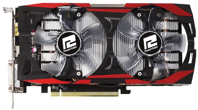 It turns out that the R9 Nano simply has no direct competitors, this model is unique and stands apart on the market.
Like the Fury elite family of video cards, the Nano features 4 GB of video memory, which is enough even for high resolutions at maximum quality settings, although a number of modern games require 4K resolution and full-screen anti-aliasing with high quality settings enabled. even more volume. But the first generation of HBM memory simply does not allow making a board with 8 GB of such memory, and nothing can be done about it. However, for a miniature mini-ITX board, this is not so important, and the closest competitor in the form of the GeForce GTX 970 with GDDR5 memory has the same amount of video memory, and even with some restrictions (you can only access a 3.5 GB partition at full speed).
The R9 Nano video card itself is very compact in size, the use of HBM-memory made it possible to reduce its physical dimensions and the number of components on the board — in particular, in the power circuit.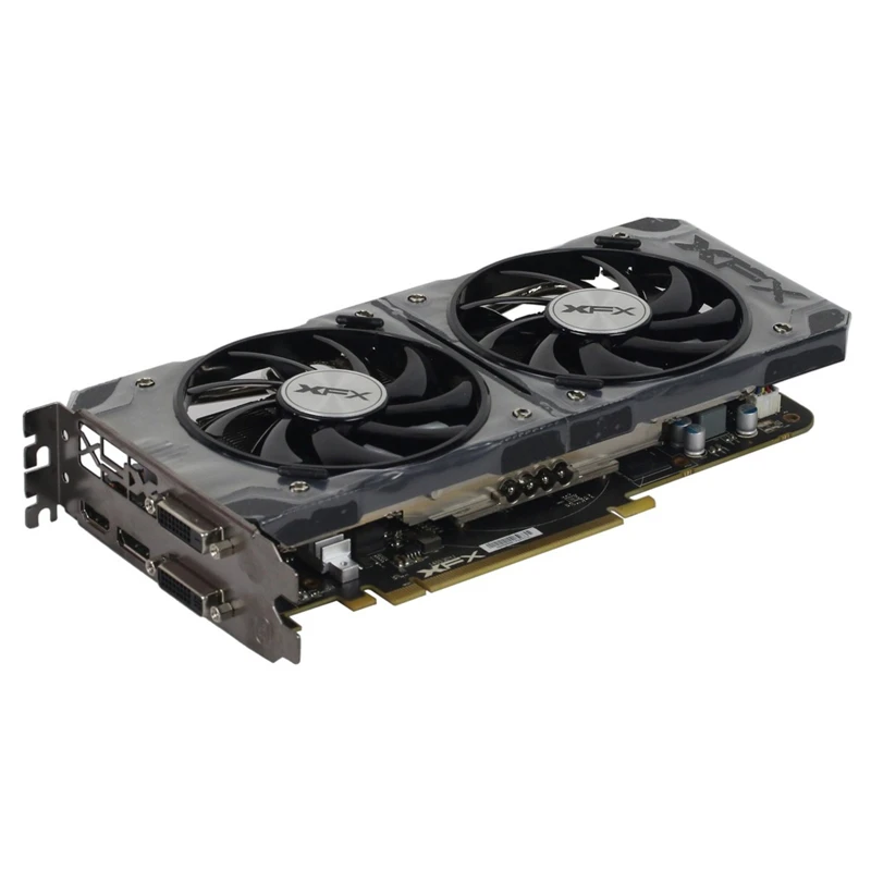 Since the Radeon R9 Nano video card in question is unique and has many interesting design features, we have deduced their detailed description in a separate chapter.
Architectural Features
The Radeon R9 Nano graphics card model is based on the full Fiji GPU that we already reviewed in the Radeon R9 Fury X review, and many details can be learned from the related material, including: architectural features, a brief overview of HBM memory , new software features including advanced DirectX 12 support, and more. It is also useful to read the material about the long-known Graphics Core Next (GCN) architecture, which underlies all modern AMD solutions.
Although the Fiji GPU has had some changes from last year’s Tonga, it is the third generation of GCN — it can be loosely referred to as version 1.2. The new top-end GPU includes all of the GCN 1.2 enhancements, including improved geometry and tessellation performance, new framebuffer lossless data compression, some 16-bit multimedia instructions, and increased L2 cache to 2 MB.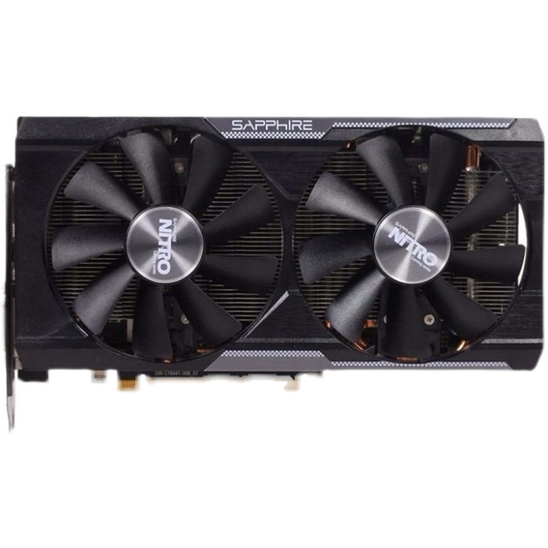 In terms of computing capabilities, the new GPU received improved scheduling and task distribution and several new instructions for parallel processing of data — all this is described in detail in the Radeon R9 review.Fury X.
Schematically, the Fiji GPU is similar to Hawaii, released back in 2013 — both GPUs are divided into four Shader Engines, each of which has its own processor for processing geometric data and a rasterizer, as well as four enlarged ROPs , capable of processing 16 pixels per clock (a total of 64 ROPs in each of these chips). The GPU has a single command processor and eight Asynchronous Compute Engines, which have been modified to reflect the changes in GCN 1.2.
Specifically, the Nano model uses a full-fledged version of the Fiji video chip — with all active units, except with a reduced clock speed of the GPU:
The Fiji graphics processor, which is installed on the Radeon R9 Fury, includes 64 Compute Units (CU) , and the total number of stream processors in this model is 4096, like in the older Fury X model.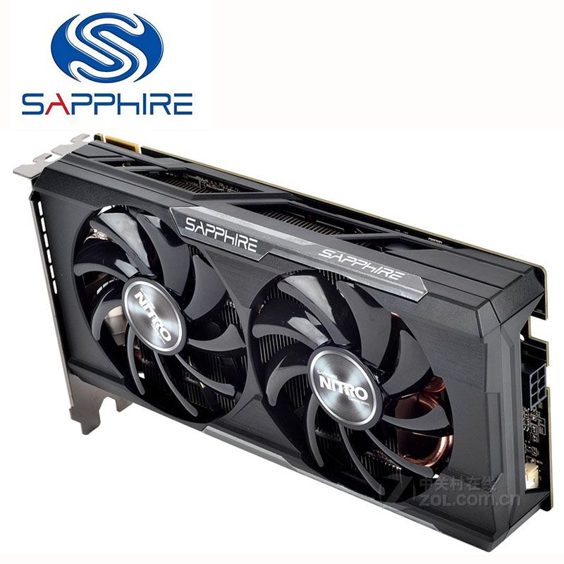 The number of texture units is the same — 256 pieces, as well as the number of geometric blocks and ROP blocks — the last ones in the chip are 64 pieces. All currently released video cards based on the Fiji chip have 4 GB of HBM memory attached directly to the GPU using 4096-bit memory bus. We published a separate material on this memory, in which all its features are considered in as much detail as possible.
Since the Fiji video chip in the R9 Nano is exactly the same as in the R9 Fury X, it has improved video processing units, etc. In particular, the Unified Video Decoder decoding unit can hardware accelerate the decoding of video data in H.265 (HEVC) format — the Fiji chip was the first discrete GPU with such capabilities. Among other advantages of Fiji, we note support for TrueAudio, LiquidVR, Mantle, Eyefinity and FreeSync technologies, which we have repeatedly written about in our articles.
From a technical standpoint, the Nano is quite impressive. Since it uses a full-fledged Fiji chip running up to 1GHz, the R9 Nano can theoretically achieve almost the same performance as the top-of-the-line Fury X, as they both have nearly identical specs including 4096 stream processors, 256 texture units, 64 ROPs and 4096-bit HBM memory.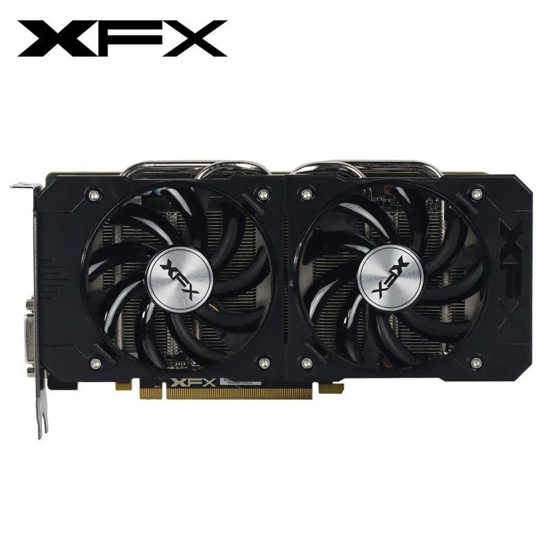 On paper, the only difference between the R9 Fury X and the R9 Nano is the maximum frequency and typical power consumption. If for R9Nano maximum frequency is set at a very high level of 1000 MHz, while for the top-end R9 Fury X, the turbo frequency reaches 1050 MHz with absolutely no problems.
Nano seems to select the very best Fiji chips for use in the Nano, which are able to operate at relatively high frequencies with relatively low GPU voltage and power consumption, respectively. At the same time, the functional blocks in Fiji were not cut down absolutely! Which is quite surprising given the R9 Nano’s power system, powered by only one additional 8-pin connector, and rated for a typical consumption of only 175 watts of power.
It seems that, based on the numbers, R9 Nano should almost keep up with Fury X. But in practice, this is only possible if the power consumption of the board does not exceed the limit of 175 W, because Fury X has much higher power — 275 W . Based on the principle of operation of PowerTune, it will be precisely the limit on energy consumption that will limit the performance in the case of Nano. Even specially selected Fiji GPUs cannot run at 1000 MHz in serious tasks with consumption limited to 175 watts — this is too tight a limit for such a powerful GPU.
Therefore, the graphics processor of the R9 Nano model in demanding 3D applications will most often operate at a frequency of about 900-920 MHz, which AMD itself confirms. They achieved a typical GPU clock speed in games of 900 MHz, and the actual value will depend on the application and its operating conditions. So, despite the beautiful figure of 1000 MHz, the Radeon R9 Nano video card is not able to support such a frequency, and in reality it will be about 10% slower.
Why, then, did the experts set such a high turbo-frequency value? AMD claims that this is done so that the board in any conditions always rests only on the consumption limit, ensuring maximum rendering speed within it. It is not very clear, however, why the video chip should work at a frequency of 1000 MHz in undemanding 3D applications, and significantly reduce the frequency where it would be nice to add it. But the figure of 1 GHz is beautiful in any case — especially for such a miniature board with a powerful GPU.
Board Design Features
The design of the Radeon R9 Nano combines all of AMD’s latest technologies to pack solid power into such a small box. And the new board looks solid, its construction uses high-quality materials, as is the case with the R9 Fury X. Many parts of the R9 Nano are also made of metal, as is customary in the premium market, and it also has a matte black PCB.
And yet, the main distinguishing feature of the Radeon R9Nano is her size. Unsurprisingly, the compact Radeon R9 Nano is perfect for demonstrating one of the benefits of HBM memory. Since four gigabytes of compact chips are installed in packs directly on the GPU core in Fiji, the total area occupied by these microcircuits on a printed circuit board is very small — three times less than previously common solutions.
And if even in the top model Radeon R9 Fury X we saw the advantage of the lack of large GDDR5 memory chips on the board, expressed in relatively modest dimensions, then the R9 modelThe Nano is even smaller in size — it is designed to install the board in mini-ITX (6.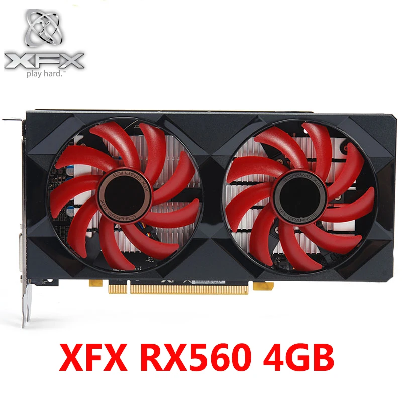 7 × 6.7 inches) format systems.
The total PCB length of the novelty is quite impressive — only 6 inches (about 15 cm), which allows the R9 Nano to be used in motherboards and cases of this format. That’s 40% shorter than the previous generation’s top 11-inch Radeon R9 290X board:
To fit into such a small footprint, AMD moved some of the power system components to the back of the PCB. Additional power for Radeon R9The Nano provides a single 8-pin PCI-Express connector, which is used instead of a pair of 6-pin connectors, also due to its comparative compactness.
The modest size of the Radeon R9 Nano allows it to be used in small form factor PCs, which are gaining popularity among gamers who want the same power in a small package without losing the ability to play at the highest resolutions and maximum settings. And the 6-inch Radeon R9 Nano is great for that, coming in cases that you can’t fit any other graphics card of similar performance into.
Here are just a couple of examples of small form factor (SFF) cases that AMD recommends for use with their new solution: Lian Li PC-Q33 (pictured) and Cooler Master Elite 110.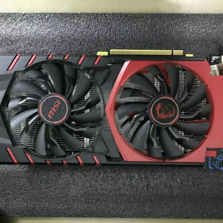 In our opinion, a very interesting option for a home gaming PC for gaming enthusiasts (not to be confused with ultra-enthusiasts and overclockers):
Cooling the Radeon R9 Nano video card is an air cooler, specially designed to remove 175 watts of heat from such a small board. The only fan is located in the center of a powerful radiator. The design of the cooler is combined: although an open fan is used, it also blows air from the side. Thanks to this solution, about half of the heat from the board is taken out to the outside of the case, although the rest of the heat remains inside — the case cooling system will take care of its output.
The Nano radiator consists of two parts. Its main part is made up of an evaporation chamber and heat pipes. The evaporation chamber is made of copper alloy, it removes heat from the Fiji core and the stacks of HBM memory installed on it, and the heat pipes effectively distribute it throughout the radiator area. The second part is a small heat sink with another heat pipe, mounted separately and cooling exclusively the MOSFET in the voltage regulator module (VRM).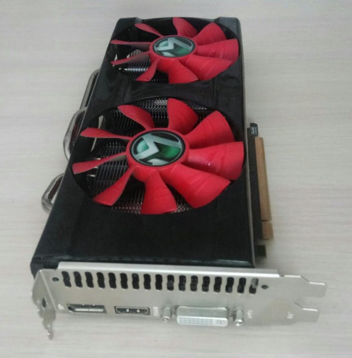
The use of the vapor chamber in the R9 Nano model is explained by the fact that such solutions are more efficient than simple radiators, in this case both the vapor chamber and heat pipes are used, which is rare in a joint solution. AMD assures that the cooling system used is very efficient, and the performance of the R9 Nano should not be limited by the GPU temperature limiter.
Tiny graphics card is designed to operate at a target GPU temperature of around 75 degrees, 20 degrees below the target temperature set for the previous generation Radeon R9 model290X, and the decrease in frequency and voltage (the so-called throttling) will begin only at 85 degrees.
In addition, AMD claims that the R9 Nano has a very quiet cooling system — they even compare the noise from it with the natural sound background in libraries. According to the company’s own measurements, the R9 Nano’s efficient air cooler powers today’s top-end GPUs at 42 dBA, a whopping 16 dBA lower than the fairly noisy Radeon R9 290X cooler.
Performance summary, positioning and conclusions
AMD itself often compares the new product with the Radeon R9 290X, the previous generation’s top-of-the-line board based on the Hawaii chip, which does not have particularly good energy efficiency and has a loud cooler. It is clear that against such a background, the R9 Nano will look like its complete opposite.
For example, in the 3DMark Fire Strike Ultra benchmark at 4K resolution, the R9 Nano delivers noticeably better performance than the Radeon R9 290X and GeForce GTX 970:
According to AMD, the R9 Nano is also 30% faster in games than the Radeon R9 290X, while consuming 30% less power (175 W vs. 250 W), and the new cooler is much quieter than the top motherboard the previous generation. Together, this gives the R9 Nano a twofold advantage in energy efficiency over the Radeon R9 290X, not to mention the much greater compactness of the novelty.
Even if we compare the Nano against other models in the Fury line, its performance should be very close, given the approximately 15% lower typical GPU operating frequency compared to the Fury X.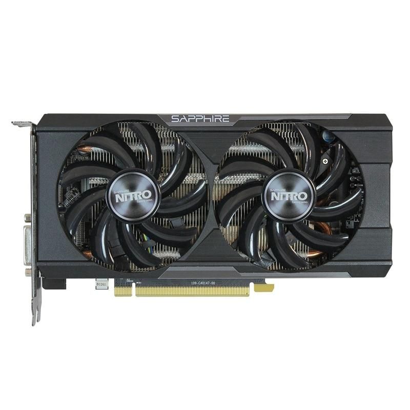 That is, the miniature R9Nano will provide about 85% of the speed of the top board in the current AMD line, and the “airy” Fury on a stripped-down Fiji overtakes it by only 8%, based on theory. So in terms of speed, the new product should be somewhere between the Radeon R9 390X and R9 Fury.
However, these models were clearly not the main target for AMD when releasing the R9 Nano. The miniature model is made to be the most powerful mini-ITX graphics card on the market. Among its compact competitors, the most productive models are the Radeon R9280 and GeForce GTX 970, there is also a GTX 960, but it is much slower.
In particular, ASUS has a compact version of the GeForce GTX 970 in its lineup, which is closest to the R9 Nano in terms of size and performance. But this video card from Nvidia is based on a non-top-end GM204 chip, and is clearly inferior even in theory to a full-fledged Fiji, even if in reality it operates at a frequency of only about 900 MHz. On average, AMD estimates the advantage of their solution at 30%, provided rendering in 4K resolution, of course (when the GeForce starts to suffer from a lack of video memory):
AMD’s GeForce GTX 970 and Radeon R9 290X are pretty close in almost all games, with the R9 Nano significantly faster than both.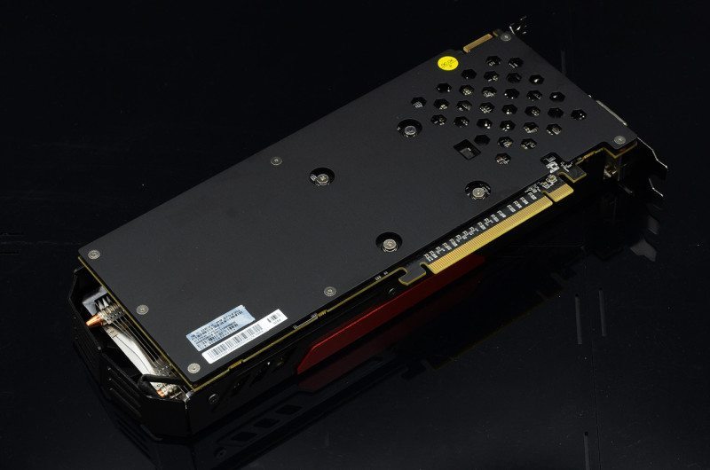 Although the advantage of the Nano will differ in different conditions, on average, the Radeon R9 Nano can be safely called the most powerful among mini-ITX video cards. Interestingly, in the conditions of cramped cases, the advantage of the R9 Nano is even higher — due to low heat dissipation and thoughtful cooling, it does not reduce the frequency when overheating.
These slides indicate the loss in orange when going from testing in an open area to a closed cramped mini-case. And, judging by a couple of gaming tests from AMD, the performance of their new product in small SFF cases practically does not decrease, while the mini-ITX version of the GTX 970 significantly reduces the frequency of the GPU, which results in the loss of precious frames per second.
In general, in terms of computing and gaming performance, everything is fine with the new product, the R9 Nano is simply the best in its class, but the price remains an important issue. Especially considering the special selection of the best Fiji video chips, which are already very expensive to manufacture, especially because of the HBM memory.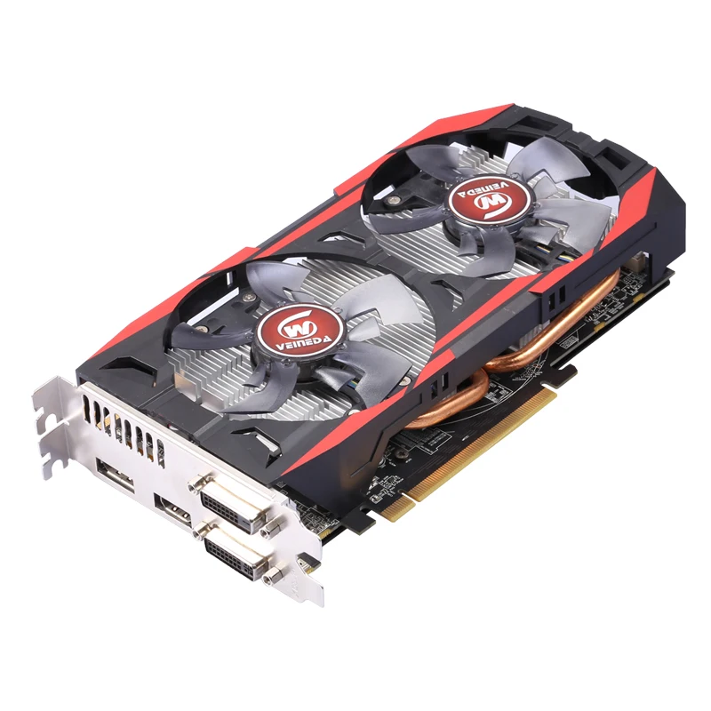 In addition, an advanced cooler with a vapor chamber is installed on the board, which also adds a lot to the cost.
So it’s not surprising that AMD is positioning the R9 Nano as another premium series graphics card, similar to Nvidia’s Titan. After all, R9 Nano has unique characteristics, offering hitherto unattainable performance in the mini-ITX market. Therefore, the price of the new product was set quite high — as much as $649 for the US market, exactly like the older water-cooled Fury X. Let’s hope that this will allow AMD to improve its financial position. True, so far the market for mini-ITX solutions is quite small compared to the market for large gaming PCs, but there is hope for its further growth.
Considering the difficulty of selecting video chips suitable for R9 Nano operation, the question of the availability of the solution on the market also arises — will AMD be able to supply a sufficient number of such boards to retail networks? And here the R9 Nano will help that the market for gaming mini-PCs is not too large, and they should be able to cope with the supply of the video card in question for $650.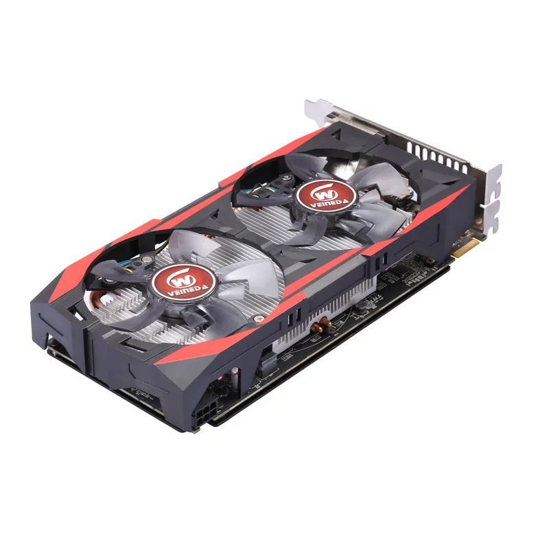 Moreover, the situation with the production of Fiji chips is constantly improving, more and more of them are being produced, and there is no longer a severe shortage on the market.
The Radeon R9 Nano introduces a new class of powerful graphics cards in small sizes suitable for installation in tiny mini-ITX cases. At the same time, the novelty is up to 30% faster while consuming 30% less energy than the top model of the previous generation Radeon R9 290X. Yes, and the top R9 Fury X in terms of speed, it will yield quite a bit. All in all, at just 175W, the Radeon R9 Nano is the most energy efficient and powerful board in the mini-ITX graphics card market segment. It also has a minimal size and a very efficient air cooler. All together, this allows you to create the most powerful small form factor gaming PCs that were simply not possible before.
Graphic accelerators of the Radeon R9 390 series (x)
| Code name | Grenada (Hawaii) | ||||||||||||||||||||||||||||||||||||||||||||||||||||||||||||||||||||||||||||||||||||
| Production Technology | .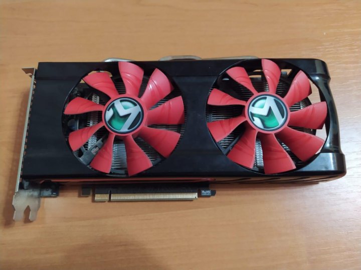 |
||||||||||||||||||||||||||||||||||||||||||||||||||||||||||||||||||||||||||||||||||||
| Architecture | Unified, with an array of common processors for stream processing of multiple types of data: vertices, pixels, etc. | ||||||||||||||||||||||||||||||||||||||||||||||||||||||||||||||||||||||||||||||||||||
| DirectX 9 hardware support0017 | The level of capabilities Feature LEVEL 12_0 and the shader model Shader Model 5.0 | ||||||||||||||||||||||||||||||||||||||||||||||||||||||||||||||||||||||||||||||||||||
| Memory bus | 512-bit: Eight controllers with width of 64 bits with GDDR5 | Up to 1050, MSC Frem | |||||||||||||||||||||||||||||||||||||||||||||||||||||||||||||||||||||||||||||||||||
| Compute Units | 44 GCN Compute Units including 176 SIMD cores, consisting of a total of 2816 Floating Point ALUs (Integer and Float formats are supported, with FP32 and FP64 precision) | ||||||||||||||||||||||||||||||||||||||||||||||||||||||||||||||||||||||||||||||||||||
| Texture units | 176 texture units, with support for trilinear and anisotropic filtering for all texture formats | ||||||||||||||||||||||||||||||||||||||||||||||||||||||||||||||||||||||||||||||||||||
| ROP units (ROP) , including with FP16 or FP32 framebuffer format. Peak performance up to 64 samples per clock, and in colorless mode (Z only) — 256 samples per clock | 64 | ||||||||||||||||||||||||||||||||||||||||||||||||||||||||||||||||||||||||||||||||||||
| Effective memory frequency, MHz | 6000 (4 × 1500) | ||||||||||||||||||||||||||||||||||||||||||||||||||||||||||||||||||||||||||||||||||||
| Memorial type | GDDR5 | ||||||||||||||||||||||||||||||||||||||||||||||||||||||||||||||||||||||||||||||||||||
.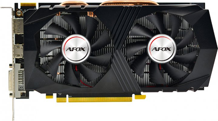 s s |
384 | ||||||||||||||||||||||||||||||||||||||||||||||||||||||||||||||||||||||||||||||||||||
| Computational performance, Teraflops | 5.9 | ||||||||||||||||||||||||||||||||||||||||||||||||||||||||||||||||||||||||||||||||||||
| Theoretical maximum fill rate, Gigapixels/s | 67 | 0016 GDDR5 | |||||||||||||||||||||||||||||||||||||||||||||||||||||||||||||||||||||||||||||||||||
| Memory volume, GB | 8 | ||||||||||||||||||||||||||||||||||||||||||||||||||||||||||||||||||||||||||||||||||||
| Memory capacity, GB/s | 384 | ||||||||||||||||||||||||||||||||||||||||||||||||||||||||||||||||||||||||||||||||||||
| 64 | |||||||||||||||||||||||||||||||||||||||||||||||||||||||||||||||||||||||||||||||||||||
| Theoretical texture sampling rate, Gtexels/s | 160 | ||||||||||||||||||||||||||||||||||||||||||||||||||||||||||||||||||||||||||||||||||||
| Bus | PCI Express 3.0 9300, only the Fury, Fury X and Nano models can be noted, and we already knew the rest from the previous generation.
In fact, a pair of video cards of the Radeon R9 390(X) subfamily is not much different from similar models of the previous series represented by the Radeon R9 290(X). The naming system for AMD video cards has long been established and the new video cards were named the same, except for the first digit indicating the new generation of the series. With the exception of some characteristics of the new products of 2015, practically nothing has changed in them — these are all the same video cards based on the Hawaii GPU we have long known (now it is called Grenada, but this has not changed much). Among the changes, we can note a slightly increased frequency of the GPU: from 1000 to 1050 MHz for the Radeon R9 390X and about the same 50 MHz for the younger model R9 390. This change cannot be called serious, given that many video card manufacturers released factory overclocked versions R9 290(X). Of the more important changes, we single out the changed volume and frequency of video memory. If previous similar models of AMD video cards had GDDR5 memory of four gigabytes and a frequency of 5000 MHz, then the current series has doubled the volume to 8 GB, and the frequency has increased to 6 GHz. On the one hand, 4 GB of GDDR5 memory is still enough in the vast majority of games even at maximum quality settings, and even the top Fury and Fury X have exactly this amount of memory, although of a different type — HBM. But, on the other hand, projects are already coming out in which 4 GB is not enough when it comes to rendering resolution above FullHD and maximum settings, like Call of Duty: Black Ops 3 — in this game, at ultra-high settings, the Radeon R9 390 is even faster than R9 Fury X precisely because of the lack of video memory in the latter. As for the 20% increase in memory clock speed, this can also be called a good increase, since Hawaii in modern games sometimes runs into memory bandwidth and does not show the performance that video cards based on it are capable of. Otherwise, there are no more differences, even the typical power consumption of these «new» models has not increased — it remains at the level of 275 watts. You can find all other details about these video cards in the articles on Radeon R9 models.290(X). Graphic accelerators of the Radeon R9 380 series 380 (x)
Curiously chosen name in the new line for the model in question — after reviewing the market positioning of the entire series, this video card was excluded from the Radeon R9 seriesand moved down to the Radeon R7 subfamily. Actually, a copy of this model from the Radeon 200 family was also in the R7 subfamily (R7 265), but the R9 270 model belonged to a more serious subfamily. A rather strange decision, since nothing has changed in terms of performance in the “new product”. The Radeon R7 370 sits at the bottom of the company’s product line, based on the Pitcairn GPU, also known as Curacao. This is one of the oldest GPUs used in the new Radeon 300 line, such models as the Radeon HD 7850 and R7 265 are based on a chip with exactly the same characteristics. Well, except that the «new» is slightly overclocked compared to its predecessors — up to 1050 MHz for GPU and 5700 MHz for GDDR5 memory. But in terms of performance, it remains very close to the models of previous generations already known to us. AMD is positioning its nominally new solution as a rival for the Nvidia GeForce GTX 750 Ti, which is not surprising, given that the Radeon R7 265 was also a rival for the same model. It is likely that two versions of this new model will appear on the market: with 2 and 4 GB of video memory, which also differ in retail prices. Two gigabytes is still most often enough for resolutions up to 1920×1080(1200), but some modern games require more at high quality settings. The graphics card itself is small in size and, like its predecessor, the Radeon R7 265, is equipped with only one six-pin auxiliary power connector, which means a power consumption level of about 150 watts. This value clearly indicates the use of an outdated GPU, which is not very energy efficient, because the competing GeForce GTX 750 Ti graphics card with a very energy efficient Maxwell architecture video chip consumes only up to 60 watts. The exterior design of the Radeon R7 370 cooling shroud emphasizes commonality with other models of the new line, and among the connectors on it you can find two DVI ports and full-size HDMI and DisplayPort video outputs. Although the characteristics of the reference board are not particularly important, since AMD partners offer their own options with the original design of printed circuit boards and cooling systems, which may also differ in the set of image output connectors. New Model FeaturesSince the Radeon R7 370 is based on the Pitcairn/Curacao GPU we’ve covered so many times, this section will be extremely brief. To get started, you can read the material about the long-known Graphics Core Next (GCN) architecture using the Tahiti chip as an example. All of the company’s modern solutions are based on this architecture, and even more modern GPUs feature minor modifications in computing capabilities, some additional DirectX 12 features and advanced AMD PowerTune technology, while the basics remain unchanged. The Radeon R7 370 is based on a reduced Pitcairn/Curacao chip. In this modification of the graphics processor, four computing devices are disabled (out of 20 computing devices, 16 remain active). This gives a total of 1024 stream processors instead of 1280 ALUs for the full version. The same applies to texture units: their number has been reduced from 80 TMUs to 64 TMUs, since each GCN unit has four texture units. In terms of the number of ROPs and memory controllers, these chips are the same, they have 32 ROPs and four 64-bit memory controllers, giving a common 256-bit bus. The operating frequencies of the video card of the new Radeon R7 370 model are slightly higher than those of the R7 265, and even more so higher than the frequencies of the Radeon HD 7850. The graphics processor in this model received a frequency of 1050 MHz, and the video memory of the novelty operates at a frequency of 5.7 GHz. The use of fast GDDR5 memory gives a bandwidth of 182 GB / s, which is quite high for this price segment, which can have a positive effect when rendering at high resolutions. The memory capacity of this model can be 2 or 4 GB, the lower value is logical for a budget video card, and the upper one can help when using 4K monitors. The newly released Radeon R7 370 graphics card supports all the same technologies as previous models based on the same GPU. We have repeatedly written about all the new technologies supported by AMD graphics chips in the corresponding reviews. In particular, the video card in question has support for the new Mantle graphics API, which helps to effectively use the hardware capabilities of AMD GPUs without being limited by the shortcomings of the existing graphics APIs: OpenGL and DirectX. As for the performance of the new model, it can yield up to 20% to older models based on the same Pitcairn chip, which is explained by the different number of active GCN execution units. The additional four CUs give the older GPU greater theoretical peak math and texture sampling and filtering performance, although they are equal in ROP performance and video memory bandwidth. But in general, the new product is slightly faster than the Radeon R7 265, although the difference between them is very small. When it comes to competing with Nvidia, the Radeon R7 370 doesn’t change much in the market, although it remains an interesting option for its class. Traditionally, at this price, AMD solutions are opposed by the GeForce GTX 750 Ti video card from the Californian company, which has a slightly lower performance. AMD is talking about 20% more performance compared to the Nvidia board, which sells for about the same money. It is clear that the Radeon R7 370 belongs to the range of the most affordable solutions costing up to $150, so there is no need to demand any special characteristics and high performance from it. This is also indicated by the assignment of the new model by AMD to the Radeon R7 series. While this level of performance is clearly not enough for PC gaming enthusiasts, typical users will be pleased with the speed they get for little money, because the presented Radeon R7 370 model is one of the best deals in its price range. Another thing is that those interested in 3D graphics would like something really new from AMD, and not a three-year-old graphics processor that comes out under a third name. There is nothing wrong with renaming old GPUs under the guise of new models, as long as it is justified from a market point of view. |
||||||||||||||||||||||||||||||||||||||||||||||||||||||||||||||||||||||||||||||||||||
| Memory bus | 128-bit: two memory controllers with width 64 bits with memory support GDDR5 | ||||||||||||||||||||||||||||||||||||||||||||||||||||||||||||||||||||||||||||||||||||
| Frequencies of the graphic processor, MHz | to 1050 | ||||||||||||||||||||||||||||||||||||||||||||||||||||||||||||||||||||||||||||||||||||
| Cumoculating blocks | 12 (from 14 Physical GCN computing units, including 48 (out of 56) SIMD cores, consisting of a total of 768 (out of 896) ALUs for floating point calculations (integer and floating formats are supported, with FP32 and FP64 precision) | ||||||||||||||||||||||||||||||||||||||||||||||||||||||||||||||||||||||||||||||||||||
| Texture units | 48 (of 56) texture units, with support for trilinear and anisotropic filtering for all texture formats | ||||||||||||||||||||||||||||||||||||||||||||||||||||||||||||||||||||||||||||||||||||
| ROP units (ROP) 16 samples per pixel, including with FP16 or FP32 framebuffer format. |
16 | ||||||||||||||||||||||||||||||||||||||||||||||||||||||||||||||||||||||||||||||||||||
| Effective memory frequency, MHz | 6500 (4 × 1625) | ||||||||||||||||||||||||||||||||||||||||||||||||||||||||||||||||||||||||||||||||||||
| Type of memory | GDDR5, 128-bit | ||||||||||||||||||||||||||||||||||||||||||||||||||||||||||||||||||||||||||||||||||||
| Memory volume, GB | 2 | 2 | |||||||||||||||||||||||||||||||||||||||||||||||||||||||||||||||||||||||||||||||||||
| 104 | |||||||||||||||||||||||||||||||||||||||||||||||||||||||||||||||||||||||||||||||||||||
| Computational performance (FP32), teraflops | up to 1.61 | ||||||||||||||||||||||||||||||||||||||||||||||||||||||||||||||||||||||||||||||||||||
| Theoretical maximum fill rate, gigapixels/s | 16.8 | ||||||||||||||||||||||||||||||||||||||||||||||||||||||||||||||||||||||||||||||||||||
| Theoretical speed of selection of textures, gigate colleges/s | 50.4 | ||||||||||||||||||||||||||||||||||||||||||||||||||||||||||||||||||||||||||||||||||||
| PCI Express 3.0 | |||||||||||||||||||||||||||||||||||||||||||||||||||||||||||||||||||||||||||||||||||||
| Senisions | One HDMI 1.4A 1.4APPPPP | Typical W | 100 | ||||||||||||||||||||||||||||||||||||||||||||||||||||||||||||||||||||||||||||||||||
| Auxiliary power | one 6-pin connector | ||||||||||||||||||||||||||||||||||||||||||||||||||||||||||||||||||||||||||||||||||||
| Number of system chassis slots | 2 | ||||||||||||||||||||||||||||||||||||||||||||||||||||||||||||||||||||||||||||||||||||
| MSRP for the US market is $109 | |||||||||||||||||||||||||||||||||||||||||||||||||||||||||||||||||||||||||||||||||||||
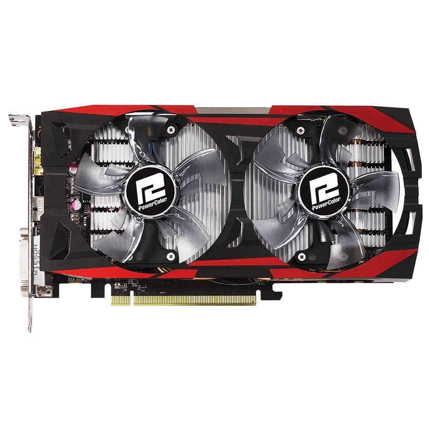
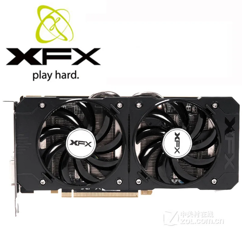 So the decision to equip this pair of video cards with double the volume can only be welcomed.
 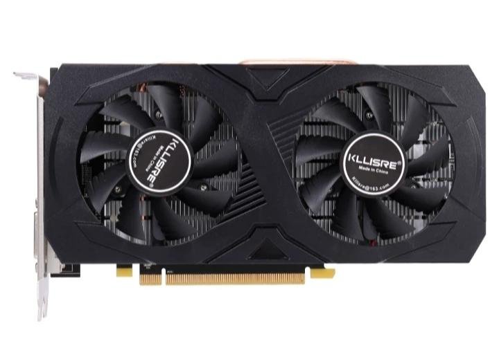 0
0 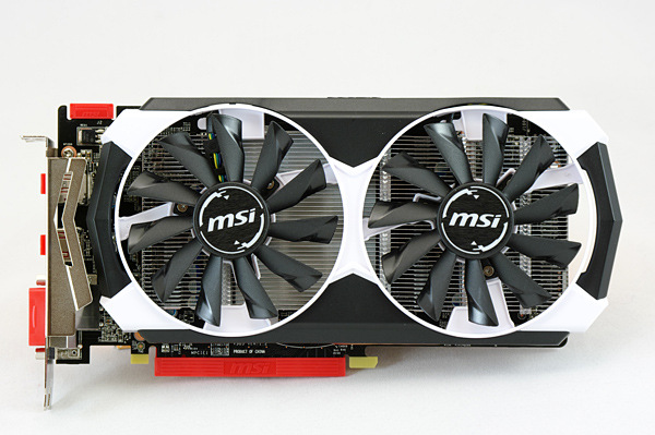 4
4  The memory bus is 256-bit, and you can put 1, 2 or 4 GB on it. One gigabyte has long been too little, and in the latest games at maximum quality settings, even in the most common FullHD resolution, two gigabytes are already missing. Therefore, a completely logical and justified decision was made to install 4 GB of video memory on the Radeon R9380X — now this value can be considered the «golden mean».
  Most video card manufacturers use the design of similar cards of the lower model Radeon R9 380, as they are very similar.
  So, in the new architecture, instructions for a heterogeneous architecture (Heterogeneous System Architecture — HSA), support for a larger number of simultaneously executed command streams appeared, DirectX 12 introduced support for the Feature Level 12_0 feature level, and a new version of AMD PowerTune technology was also introduced, about which we already told.
 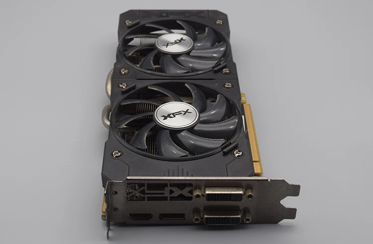 Each of these blocks deals with planning and distribution of work independently. Let’s see how a full-fledged version of Antigua/Tonga looks schematically:
 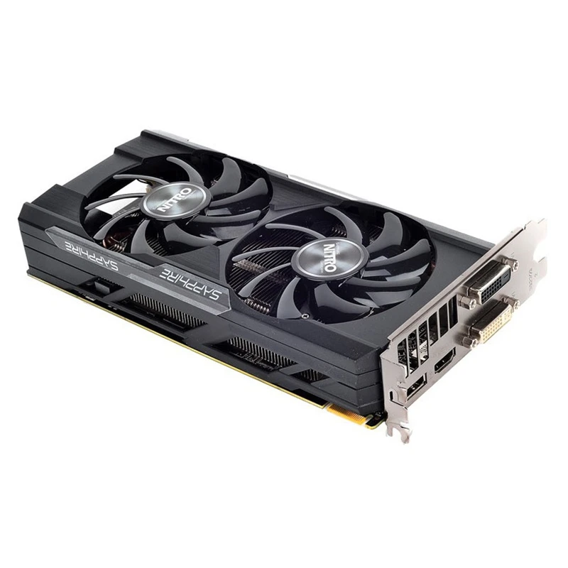 The Antigua/Tonga GPU supports the latest version of PowerTune, providing the highest possible 3D performance within a given power consumption. In applications with high power consumption, the GPU can reset the frequency below the nominal, resting on the power consumption limit, and in gaming applications it provides a higher operating frequency — the maximum possible under current conditions.
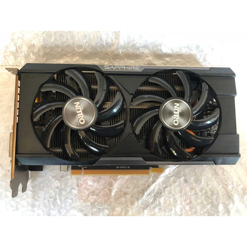 For the latest game projects, 2 GB is clearly not enough, so on the released Radeon R9The 380X decided to increase the amount of video memory from 2 GB to 4 GB, and this is a completely logical and correct decision. And although manufacturers offer variants of the R9 380 model with 2 and 4 GB of memory, the former are much more common.
 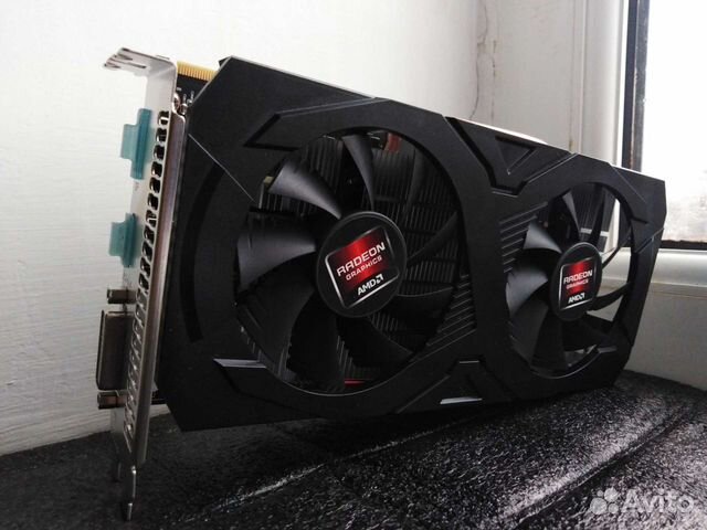 As for the competitor from Nvidia, the Radeon R9 380X does not have a direct rival in price, but is between two GeForce models: GTX 960 and GTX 970, but a little closer to the first. Comparison is better with GTX 960, especially in 3DMark Fire Strike, which is what AMD does:
 So, in general, the Radeon R9 380X quite accurately corresponds to the familiar concept of AMD, offering its video cards of comparable performance a little cheaper than its rival, or releasing video cards with a similar price, but a little faster. This concerns only the ratio of price and performance, in terms of energy efficiency, AMD solutions are still far from the latest Nvidia video cards.
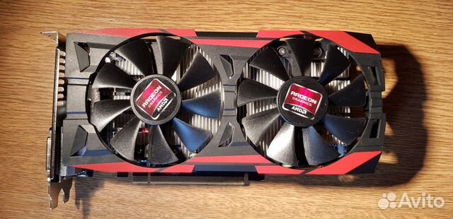 15
15  Unless AMD decided to “brush” the naming system for their video cards a little, making it more slender.
  True, for such an inexpensive video card, installing a larger amount of rather expensive GDDR5 memory simply does not make sense, because the rendering speed will be limited by the capabilities of the GPU, first of all.
 The Radeon R7 series in the new AMD line is represented by two models: Radeon R7 360 and R7 370. , is similar to the previous Radeon R7 260 line, with the graphics chip frequency increased by 50 MHz and the memory frequency by 125 MHz. Along with the increase in clock frequencies, the typical graphics card power consumption (TDP) has slightly increased — from 95 to 100 watts.
With an MSRP of $109, this model is a direct replacement for the Radeon R7 260, which is similarly priced as the bottom model of the discrete GPU lineup. As for the competitor’s solutions from the same price segment, the Radeon R7 360 model is opposed by the Nvidia GeForce GTX 750, based on the stripped-down GM107 chip, and the full-fledged version in the form of the GTX 750 Ti competes with the Radeon R7 370.
So the main price competitor for The Radeon R7 360 is a video card of the GeForce GTX 750 model. Indeed, in many respects they are similar, and in terms of speed, the Radeon even has some advantage. True, the GeForce GTX 750 consumes only 55 watts and does not even require an additional power connection — thanks to the highest energy efficiency of the Maxwell architecture, albeit in the form of its first generation.
The considered model of the video card has GDDR5 memory with a capacity of 2 gigabytes, which is great for it, given the focus on FullHD resolution and the budget price segment. Since this GPU has a 128-bit memory bus, it would theoretically be possible to put both 1 GB and 4 GB on it, but a smaller amount by modern standards is already completely insufficient, and 4 GB of fast GDDR5 memory is too expensive for the lower price segment. And 2 GB should be enough for most games at playable settings.
The design of AMD’s reference Radeon R7 360 board is very simple, the most simplified cooler with an aluminum heatsink and fan is used as a cooling system, although the cooling system still remains a two-slot one. For additional power, one 6-pin connector is used, and the image output ports on the board are equipped with two DVI and one each for HDMI and DisplayPort. However, most manufacturers of such solutions still released their boards with their own design of both PCB and coolers, so the reference one is not so important.
Architectural and design features
The graphics card of the Radeon R7 360 model is based on the Tobago chip, also previously known to us from the Radeon HD 7790 as Bonaire, but not in its full configuration. This chip modification contains 12 active Compute Units of 14 pieces physically present in the graphics processor — everything is exactly the same as in the Radeon R7 260 model. The Bonaire graphics processor belongs to the second-generation Graphics Core Next (GCN) architecture that we have long known (conditionally it can be called GCN 1.1), in which some changes have been made.
The chip is architecturally not too different from the first generation GCN, but many useful improvements have indeed been made to it. So, in the new architecture, instructions for a heterogeneous architecture (Heterogeneous System Architecture — HSA), support for a larger number of simultaneously executable threads appeared, DirectX 12 introduced support for the Feature Level 12_0 feature level, and a new version of AMD PowerTune technology was also introduced, which we have already have been told many times.
The base blocks in Tobago remained unchanged, so you can safely get acquainted with the article dedicated to the announcement of the long-standing flagship of the company Radeon HD 7970, which thoroughly described all the features of the new Graphics Core Next architecture. As you know, the basic block of the architecture is the GCN block, from which all the company’s graphics processors are assembled. The GCN computing unit is divided into subsections, each of which works on its own instruction stream, they have a dedicated local data storage, a first-level cache, and a texture pipeline with sampling and filtering units.
At the time of its introduction, the Bonaire GPU with its 14 GCN units was midway between Cape Verde with 10 compute units and Pitcairn with 20 GCN units. Bonaire has filled a niche in the middle between these solutions. The chip was later re-released under the Tobago name. The diagram shows a stripped-down GPU that is used in the Radeon R7 360 model in question. It has 12 active GCN architecture compute units, which correspond to 768 stream computing processors. And since each active GCN unit has 4 texture units in its composition, the final figure for the number of TMUs for the model under consideration is 48 texture sampling and filtering units.
But in terms of the number of ROPs and memory controllers, the chip for the Radeon R9 360 was not cut, as in the case of the R7 260. There are 16 active ROPs, and the chip’s memory bus is 128-bit, assembled from two 64-bit channels. The use of a relatively fast GDDR5 memory made it possible to provide a sufficiently high bandwidth for a video card of the lower price segment, which was also further increased in the solution of the new line, reaching a value of 104 GB / s.
Similar to other models in the current Radeon 300 line, the Radeon R7 360 provides slightly better performance than its counterpart in the Radeon 200 family. In this case, AMD raised the GPU and video memory frequencies from 1000 MHz and 6 GHz to 1050 MHz and 6. 5 GHz compared to the Radeon R7 260. It should be understood that 1050 MHz is the maximum GPU turbo frequency for the reference model, in partner video cards and real 3D applications the value may be different.
Although the video chip is not new, it supports many AMD technologies, here is a partial list: PowerTune, ZeroCore, Eyefinity, HD3D, etc. We wrote about all this earlier in articles about the oldest chips in the GCN family, and the Tobago/Bonaire-based model supports all of these features, including AMD Eyefinity 2.0 technology with support for six monitors with stereo rendering. Also, this GPU is distinguished by an improved block for decoding and encoding video data, although in terms of its capabilities it is no longer new.
Performance Summary and Conclusions
As for the performance of the Radeon R7 360, we can safely say that it should be approximately equal to the speed of the Radeon R7 260, because the increase in the maximum frequency of 50 MHz is unlikely to give a noticeable increase in the average frame rate, given that this is only the maximum turbo frequency of the GPU, and the increase in memory bandwidth is not so significant.
We are rather more interested in comparison with a competitor, which is the GeForce GTX 750 video card model from Nvidia. To begin with, let’s look at a comparison of two pairs at once: two models of the Radeon R7 300 subfamily and competing Nvidia video cards in the 3DMark Fire Strike synthetic benchmark at a resolution of 1920×1080.
Interestingly, AMD opted for 4K resolution for the Radeon R9 390X and R9 390, 1440p for the Radeon R9 380, and 1080p for the R7 300 line. Moreover, the older Radeon R7 370 should provide an acceptable rendering speed at high settings, and the R7 360 already at slightly reduced ones. Actually, the difference between their performance is clearly visible in the diagram:
According to the company, the Radeon R7 370 is significantly more productive than the model in question, but this model is sold more expensive. But both Radeon video cards are faster than their competitors in the face of the GeForce GTX 750 Ti and GTX 750, respectively. Despite the synthetic nature of this test, approximately the same difference in favor of Radeon solutions is observed in games:
According to AMD’s tests, the Radeon R7 360 is on average faster than the GeForce GTX 750 at 1920×1080 resolution and high quality settings in a set of five popular games. Well, let’s turn again to the topic of multiplayer games popular in eSports, evaluating the rendering speed of the Radeon R7 360 and 370 in such projects: AMD provides sufficient frame rate in such applications. Even the inexpensive Radeon R7 360 and R7 370 models are capable of high frame rates in excess of 60 FPS in the most popular online games.
It can be noted that the Radeon R7 360 is AMD’s entry-level budget graphics card. It is aimed at players who are interested in multiplayer games and use lower rendering resolutions up to and including 1920×1080. Although games like DOTA 2, League of Legends, etc. usually work well on integrated graphics, AMD and Nvidia also want a piece of this pie, so they are trying to lure players with budget systems to entry-level discrete graphics cards that provide more high picture quality with better performance. And for such tasks, the Radeon R7 360 is excellent, providing excellent functionality and image quality at a fairly high rendering speed.
Radeon X
family reference information Radeon X1000 family reference
Radeon HD 2000 family reference
Radeon HD 4000 family reference
Radeon HD 5000 family reference
Graphics card family reference Radeon HD 6000
Radeon HD 7000
Family Reference Radeon 200 9 Family Reference0003 Radeon 300 Family of Graphics Card Background
AMD RDNA 2 Midrange Graphics Cards Revealed — NVIDIA WORLD
RDNA 2-based accelerators available.
Lisa Su, AMD CEO, has announced twice in the past three weeks that a powerful new GPU can take on NVIDIA’s RTX 2080 Ti. And so, the first specifications of this video card became known.
The Big Navi GPU is said to find its way into the Radeon RX 5950 XT graphics card. The chip will receive 80 computing cores, 5120 stream processors and performance at the level of 17.5 teraflops. The new RDNA2 architecture will also enable hardware-accelerated ray tracing.
But what about gaming performance? 80 compute units is double that of the Radeon RX 5700 XT. However, it is hardly worth counting on a double increase in speed. The Radeon RX 5700 XT graphics card consumes 225W, and AMD will probably have to lower the frequency to 1500-1700 MHz to reduce the appetites of the new accelerator. The TweakTown website, citing its own sources, reports that AMD did not receive such energy efficiency from the transition to 7 nm + as expected, and therefore savings are inevitable. That is why the performance of the Radeon RX 59 is expected to50 XT will be the same as the GeForce RTX 2080 Ti, the 2018 graphics card.
It takes another half a year to produce a new AMD card, but by September NVIDIA plans to release the Ampere generation, and AMD again runs the risk of falling behind.
rumorsRDNA 2video cardsNaviAMDgraphics processors
comment on similar news
They say that the RDNA 2 architecture GPU will be present in the next generation of video cards. The company should redesign these Navi 2X processors in 6nm process technology, after which they will take their place in the mid-range Radeon RX 7600 and Radeon RX 7500 graphics cards. These are Navi 24, Navi 23 and Navi 22 GPUs.
Radeon HD 6000
As for Navi 31 and Navi 33 processors based on the RDNA 3 architecture, they will be used in the top Radeon RX 7800 and Radeon RX 79 cards00.
The Navi 31 processor should form the basis of the Radeon RX 7900 XT. It will receive a multi-chip design or a multi-chip module. While the Navi 33 will already be monolithic and will find the application in the Radeon RX 7800.
rumors 23 Video -CardiamDradeon HD 7000
Comment Similar news
Tweaktown
The future GPU from AMD AMD AMD 4 times more strength than RDNA2. At least that’s what the latest rumors say.
It is noted that the company has designed a GPU with 15,360 stream processors, which is 4 times more than in the Radeon RX 6800. These stream processors are grouped into 60 workgroups, WGP — Workgroup Processors, instead of compute units. This became possible due to the fact that in RDNA3 the computing units will not be as independent as in the original RDNA and even RDNA2, in which groups of two CUs began to use common resources.
AMD
GPU Other rumors say that AMD will not play the game with NVIDIA to expand the memory access bus, but will instead improve the Infinity Cache technology by increasing the size of the cache on the core and keeping the memory bus «available» at 256 bits.
As for the chip itself, according to rumors, it will be called Navi 31, will have a modular multi-chip design with at least two logical cores of 30 WGP each. The processor will be manufactured using TSMC N5 technology, or a special 6 nm process developed for AMD.
Like NVIDIA’s next generation of Lovelace GPUs, the next generation of AMD RDNA3 is set to arrive in 2022.
rumorsRDNA 3video cardsAMDgraphic processors
comment on similar news
TechPowerUp
Some information about AMD’s new Navi 23 GPU leaked online
AMD’s smallest RDNA2 based GPU, Navi 23, has more transistors than the largest Legacy GPU, Navi 10.
This processor powers the Radeon RX 6600 series desktop graphics cards, the Radeon RX 6600M mobile graphics card, and the Radeon Pro W6600 professional graphics card. The processor contains 11.06 billion transistors, which is more than the Navi 10 in the Radeon RX 5700 XT accelerator, which has 10.3 billion transistors. At the same time, the core size of the new solution is 237 mm 2 , while the old one has 251 mm 2 .
AMD Navi 23 GPU
Made by Navi 23 using the same 7nm technology. It is based on the RDNA2 architecture and contains 32 computing units that house 2048 flux transistors. The chip also has 128 TMUs and 32 ROPs. There is also an acceleration of ray tracing.
The GPU memory subsystem is interesting. The memory bus is 128 bits wide, but the interface is associated with 32 MB of Infinity Cache memory located on the core. And it is this cache that can give a significant increase in the number of transistors. The chip supports PCI-Express 4.0, but 8 or all 16 bus channels are still unknown.
RDNA 2video cardsradeon RX 6600
graphics processors
The top-of-the-line graphics card features 32GB of GDDR6 VRAM, double that of the Radeon RX 6900 XT top gaming solution.
Based on the RDNA 2 architecture, the new graphics cards are designed for demanding professionals who work in design and architecture, develop ultra-high definition media projects, and run complex engineering simulations.
The company presented two video cards for desktop workstations and one mobile one, which, judging by the specifications, fully corresponds to the desktop version.
AMD Radeon Pro W6800 graphics card
The new generation of professional accelerators is 79% faster than the previous one. Among the benefits of the new Radeon Pro W6000 series cards, developers noted an increased number of compute units with real-time ray tracing acceleration, Smart Access Memory technologies, AMD Infinity Cache, Viewport Boost and certified ISV for leading professional applications.
(28 CU)
to 20.8 (FP16)
(28 CU)
to 20.8 (FP16)
224 (14)
224 (14)
22
The AMD Radeon Pro W6800 is already available for order at $2,250. At the same time, the Radeon Pro W6600 will be available in Q3 for a much more affordable price of $650. If you have a mobile workstation and want to upgrade, then it will be available to you from June, however, the card will not be available in all countries.
RDNA 2 video cardsAMDRadeon Pro graphics processors
According to Yuri Bubliy, the author of the CTR and DRAM Calculator for Ryzen utilities, AMD has scheduled the release of the Ryzen 5000 processors on October 20, just 12 days after their official announcement. Ryzen 7 5800X and Ryzen 9 models to launch first5900X, with the Ryzen 5 5600X and Ryzen 9 5950X coming a bit later. In addition, Yuri noted that this information is «outdated» , but AMD’s plans have not changed.
AMD Ryzen
ComputerBase also revealed that the company will ship Ryzen 5000 processors on October 20 or 27. As for the Ryzen 4000 series, the likelihood of its appearance is already minimized.
In addition to the CPU, Yuri Bubliy also announced the release of the Radeon RX 6000 series of video cards, which will take place between November 15 and 20, a couple of weeks after the AMD GPU event, which will be held on October 28.
rumorsZen 3RDNA 2Ryzen 5000Ryzen graphics cardsAMDRadeon
KitGuru
We all know that AMD is planning to release next-generation RDNA2 graphics before the end of the year. It will offer customers the same functionality that the next generation consoles have.
Early rumors said AMD RDNA2 Big Navi cards would deliver amazing performance and be NVIDIA killers. However, as the release date approaches, developers share more and more information with manufacturers, which creates a field for leaks. And now, according to such leaks, Big Navi is not as productive as expected. It is noted that it is only 15% faster than the NVIDIA RTX 2080 Ti, and then only in optimized games.
RDNA2
Considering this, AMD’s new flagship will be the main rival of the RTX 3080, which is depressing, since early rumors said that the RDNA2 flagship was 50% faster than the RTX 2080 Ti.
Apparently, AMD will have to sell the new RDNA2 at a reduced price relative to the RTX 3080, as well as lower models that will compete with NVIDIA solutions. At the same time, NVIDIA RTX 3080 Ti will become the world leader.
RumorsRDNA 2Big NaviAMDRadeonGPUs
Comment Related news
Overclock 3D
The phrase “ray tracing” has been coming out of every iron for two years now. The two main players in the gaming graphics market are preparing new solutions where this technology will be introduced.
For AMD, this is more important, because NVIDIA already has the first generation of RTX accelerators, which are represented only by mid-range and high-end models. It looks like AMD will have a slightly different situation with RDNA 2. A new GPU ID of an unknown Radeon graphics card has appeared on the Web. Apparently, we are talking about the GFX1032 GPU, which is also called Navi 23. The fact is that Navi 21 is called GFX1030, and Navi 22 is called GFX1031. But most importantly, they will all support hardware-accelerated ray tracing.
1 comment related news
TweakTown
It’s no secret that AMD is preparing a new RDNA 2 graphics architecture. In its quarterly report, the company said that new GPUs will appear this year, but so far there are only rumors about them.
Previously, it was reported that the new GPUs will provide a 50% increase in energy efficiency, which will indirectly increase performance. Fresh rumors say that the physical size of the new processors will also grow significantly.
Twitter @KOMACHI_ENSAKA reported that the Navi 21, Navi 22 and Navi 23 GPUs will be 505 mm², 340 mm² and 240 mm² respectively. This is a large size. Especially when you consider that the processor in the AMD RX 5700 XT graphics card occupies an area of 251 mm².
RDNA 2 Performance Boost
505 mm² footprint twice that of the RX 5700 XT. This also means that we can double the performance with just more transistors. The developers also promise an increase in speed due to efficiency and internal performance, which will increase the overall speed of the GPU even more than twice.
Navi 2x GPU hardware ray tracing
In addition to acceleration and lower power consumption, the RDNA 2 architecture will offer DXR compatibility, ray tracing hardware acceleration and variable shading level (VRS). This will allow AMD to reach the same technological level with NVIDIA. Moreover, RDNA 2 technologies are also used in the next generation of consoles, which means that video game developers will in most cases focus on them.
In general, the new RDNA 2 processors look very promising so far.
RumorsRDNA 2NaviAMDRadeonGPUs
Comment Related News But it turned out to be fake.
SK Hynix announced today that the published rumors are incorrect. The company assures that it did not create or distribute documentation on this issue. The company also threatened the media that carried out the misinformation with undesirable actions, including potential «lawsuits.» SK Hynix believes that such actions may be necessary for their own protection and the protection of their customers’ businesses.
Specs shown are most likely not a gaming product, and more like 7nm Vega for Radeon Instinct calculation accelerator. Perhaps because of this, SK Hynix calls the information fake.
rumorsAMDHynixRadeon graphics cards
GPUs
Overclock 3D
New post-Navi era graphics card codenamed Arcturus Radeon Inct. AMD itself called it «Server Accelerator». TechPowerUp got their hands on the BIOS for this graphics card, and here’s what they found out about it.
The device ID is indicated as «0x1002 0x738C». It is noted that the memory capacity of HBM2 will be 32 GB, and the frequency will be 1000 MHz. If a company uses a 4096-bit bus, the throughput can be as high as 1 TB/s.
The identifier line also contains the entry «MI100 D34303 A1 XL 200W 32GB 1000m». This means that the heat dissipation will be only 200 watts. Given that the card will have 128 CUs and 8192 shaders, that’s a noticeable drop. For comparison, the Radeon Instinct MI60 card with 4096 shaders has a TDP of 300W. This means that AMD has managed to increase the power efficiency in Arcturus incredibly.
Accelerator Radeon Instinct MI60
As for the frequencies of the video card, they are designated as 1334 MHz, 1091 MHz and 1000 MHz. As a rule, AMD engineers arrange them in the following order: GPU frequency, SOC frequency, and memory frequency. Thus, the GPU frequency will be 1334 MHz, noticeably lower than Navi and Vega. Perhaps lowering the frequency is necessary to improve energy efficiency.
The Arcturus card will open a new series of AMD accelerators. First it will be a series of AI accelerators, then the Radeon Pro product will be introduced, and then the client solution will appear. At the same time, Arcturus is not the promised “big Navi”. The map is much more like Vega than Navi.
rumorsartificial intelligenceVideoBIOSvideo cardsAMDgraphic processors
comment on similar news announcement, details about future video cards become known bit by bit.
According to recent rumors, new graphics cards will receive Navi 21 processors, which will be manufactured using 7 nm+ technology. It will reportedly be a large chip containing 15-16 billion transistors, more than the Vega 20 (13.2 billion) and Navi 10 (10.3 billion). However, the most interesting thing is that Navi 21-based video cards will receive from 12 to 16 GB of GDDR6 video memory, connected via a much wider bus.
AMD Navi
Now the video memory bus is said to be 384 bit or 512 bit wide, which will provide excellent throughput. Earlier rumors suggested that AMD would use the more expensive and faster 16GB or 32GB HBM2E memory. It is likely that both rumors are true, and GDDR6 memory will be seen in consumer graphics cards, and HBM2E in data center accelerators.
AMD Navi 21 graphics cards are expected to be available in the first months of this year.
rumorsgdddr6vide -card -carddographic processors
1 Comment. Similar news
Tweaktown
Fudzilla, referring to its own sources, can be made by AMD. at Samsung factories.
Thus, AMD and Samsung are collaborating not only in the development of GPUs for smartphones, but also in the field of Navi 14 computer GPUs. At the same time, the source cannot accurately determine the place of production of a particular chip, and whether all variants of Navi 14 are manufactured at Samsung factories.
Radeon 5500 XT
The fact is that the Navi 14 GPU, manufactured according to 7 nm standards, is used both in discrete desktop RX 5500 XT video cards with 22 RDNA computing units with 1408 stream processors, and in Radeon 5500M Pro video cards for 16 » Apple Macbook Pro laptops. The latter variant has 24 RDNA compute units and 1536 stream processors.
Even if AMD does order production from Samsung, this is not much of a surprise since TSMC’s 7nm production is in high demand. The company produces chips for AMD, Qualcomm, Apple, NVIDIA, Huawei, Mediatek and other customers, and therefore there is some shortage of production capacity.
Rumorsvideo cardsNaviAMDSamsungGPUsRadeon RX 5500 XT
Comment on similar news
Three variants of video cards appeared in the Compubench database under the general code GPU Navi 14. These GPUs contain 24 computing units each and oppose Polaris 11 (or Polaris 21). The boards will differ in the amount of video memory: 3 GB, 4 GB and 8 GB.
AMD RDNA
The list of identified graphics cards is as follows:
- AMD Navi 14 ‘7341:00’ 8 GB Radeon RX
- AMD Navi 14 ‘7340:C1’ 4 GB Radeon RX
- AMD Navi 14 ‘7340:CF’ 3 GB Radeon RX
Upcoming Specifications Navi 14
When AMD releases new graphics cards on the market, it will have a great trump card, because it will be able to provide hundreds of millions of gamers with video cards priced at $150-250. The lower model, with 3 GB of memory, will have the performance of the RX 560/570/580, at a price of only $150.
rumorsvideo cardsNaviAMDgraphics processors
comment on related news
TweakTown
Don’t trust everything that is written on the Internet, but rumors say that the new Navi GPU from AMD will have good performance.
As you know, the third generation of Polaris GPUs will be presented in the near future. He is the company’s only hope to get through the difficult period until the arrival of Navi in 2019.
Radeon 9 Logo0002 AMD is said to have completed development of the first version of this GPU, called Navi 12, which contains 40 compute units. New graphics aimed at gamers. Also, this architecture should be built into the new PlayStation.
In terms of performance, it will be on par with Vega 56, but at a much lower cost. According to rumors, the release of Navi 12 graphics cards will take place in the first half of 2019.
Summing up all the available information, we can assume:
- Vega 7nm will not be released for the PC market.
- Navi 10 has been canceled or moved to the end of 2019.
- Navi 20 will be the next high-end architecture expected in late 2020 or 2021.
- Navi uses post-GCN architecture.
rumorsvideo cardsNaviAMDgraphic processors
ChipHell.
The report states that the Polaris 30 will be manufactured using the 12nm finFET process and will provide a 20% performance boost over the high-end Polaris 20 GPUs released a year ago.
It is also noted that Navi architecture GPUs aimed at mid-range graphics will appear before high-performance solutions based on HBM2 memory.
AMD Radeon Vega
graphics card The Navi architecture should replace the Vega. It is possible that these GPUs will be manufactured according to 7nm standards and will first of all be sharpened for use in future generation game consoles.
In general, AMD does not change its traditions, using different microarchitectures in different price segments, unlike NVIDIA, which prefers to simplify the chip structure within the same microarchitecture.
Rumors12nm graphics cardsAMDPolarisGPUs
comment on related news
Inquirer
It looks like things that will happen in the video card world in the coming months will turn out to be quite interesting. And it’s not just the GTX 1080 Ti, which will be released in March, but also the release of video accelerators codenamed Vega from AMD, which are rumored to appear in May.
According to recent rumors, the first Vega 10 GPU will appear in May with two different graphics cards. The Vega 11 line of accelerators will also be introduced, replacing the current Polaris cards.
In addition to the release of traditional high-end Vega cards, the company also has to introduce two-chip accelerators, but they will be the last to be released.
The first solution should be a Vega 10-based card that will compete with the NVIDIA GTX 1080. Apparently, this chip will be paired with 8 or 16 gigabytes of HBM2 memory with a 512 GB / s interface. The GPU itself will get 4096 stream processors and 24 teraflops of performance while consuming 225 watts.
rumors Vegavideo cardsAMDgraphic processors
comment on similar news
Thus, it refers to the code names Baffin and Ellesmere and explains that the latter will be called Polaris 10, while the junior solution will be called Polaris 11. The driver describes at least six Polaris 11 video cards and two with Polaris 10 GPUs.
The hardware ID of one of the Polaris 10 cards is 67DF. The model will receive 36 computing units, 2304 stream processors, a core frequency of 800 MHz, a 256-bit wide memory bus and 8 GB GDDR5 memory with a frequency of 6000 MHz. These cards will replace the Radeon Rx 3xx series and become a truly high-performance replacement for current solutions. Thus, Vega is unlikely to appear before the summer of 2017.
Of course, these specifications do not pull at the fastest solution, but this is only one of the Polaris 10 cards, so we will probably see higher performance solutions.
RumorsAMDPolaris video cardsGPUs
Comment on related news
Dark Vision Hardware
VideoCardz has published a declaration listing several AMD GPUs.
As usual, the information is obtained from the customs declaration in the Zauba service, and it shows some printed circuit boards with the code names Baffin XT 4GB, Weston X3 2GB, Banks Pro S3 2GB and Weston Pro S3 2GB.
What lies behind these names is not known for certain, but most likely, we are talking about a number of video cards of the medium and budget segments. For example, the Baffin GPU could be the Radeon R7 470, Weston could be the basis for the Weston Radeon R7 460 and R5 450, and Banks could be the R5 440 accelerator.
Very little is known about these cards. According to our colleagues at VideoCardz, Weston and Banks graphics could be a 28nm rebrand, as well as Ellesmere should be similar to Hawaii, but with GDDR5X memory. Thus, only high-end Greenland and mainstream Baffin-class accelerators will become processors manufactured using the 14 nm process. But whether Hawaii will be able to benefit from the new memory is difficult to say, but it is unlikely that the performance gain will be high.
rumorsvideocardsAMDgraphics processors
comment on related news
Videocardz
Over the past couple of days, there have been many rumors that AMD is actively preparing new video cards.
A new product designed to compete with the NVIDIA GTX 780 Ti will use high-bandwidth memory, or HBM for short. This technology uses many stacked DRAM cores bundled into one package to reduce power consumption, reduce temperatures and free up usable PCB space. Stacked HBM memory exists in three versions: 2Hi, 4Hi and 8Hi, which corresponds to the number of layers in the stack.
What is known now is that the new Volcanic Islands family product will use the first generation of HBM. The first variant on the way is 4Hi memory, which has a bandwidth of 128 GB/s across four DRAM layers. Each module has a capacity of 1 GB, so with 4 of these modules, you can get a throughput of 512 GB / s.
An interesting detail of the recently leaked information is also a kind of roadmap for future AMD products. So, the Volcanic Islands series will be replaced by Pirate Islands, sometime in the second half of next year. These will be the first chips manufactured using the 20 nm process technology, which means that AMD will have to wait even more than a year before this technology appears in AMD. At the same time, 20 nm will not linger for a long time. Already in the next generation, Pirate Islands Refresh, which will be released in late 2016, the company will use a 14 nm production rate.
Future AMD GPUs and release dates are listed below:
- 28nm TSMC 1H 2014 : Hawaii, VI 1.0.
- 28nm GlobalFoundries 2H 2014 : Iceland and Tonga, VI 2.0.
- 28nm GlobalFoundries 1H 2015 : Maui, VI 2.0.
- 20nm GlobalFoundries 2H 2015 : Fiji and Treasure, PI 1.0.
- 20nm GlobalFoundries 1H 2016 : Bermuda, PI 1.0.
- 14nm GlobalFoundries 2H 2016 : Mid-GPU and Low-GPU, PI 2.0.
- 14nm GlobalFoundries 1H 2017 : High-GPU, PI 2.0.
At the same time, we should not forget that these are all rumors, but they raised such a fuss that they are probably not far from the truth.
The pictures show the improvements associated with the HBM memory, and it is not entirely clear why this new memory is needed, because even the bandwidth in the R9-series cards should be enough for future generations.
rumorsvideo memoryvideo cardsAMDgraphic processors
comment on similar news
Guru of 3D
TSMC’s 20nm process seems to be making very little progress, and NVIDIA and AMD, longtime customers of this factory, are in danger of not being able to produce next generation GPUs at all. As a result, NVIDIA had to start producing new Maxwell GPUs under the old 28nm production standards.
It is unlikely, but possible, that Maxwell processors are so efficient that they do not need an improved process technology, other than this, the use of old equipment saves money. Be that as it may, but NVIDIA this month begins the release of the first samples of the GM204 and GM206 processors using the old proven 28 nm process technology. The video cards themselves based on these GPUs are not expected before the 4th quarter of this year.
The GM204 chip should become the successor to the GK104, which will be installed in video cards from the company’s performance segment priced from $250 to $500. It is rumored to contain 3200 CUDA cores. It is expected that video cards based on it will appear at the end of the year. Another processor, GM206, will be aimed at the middle segment. And although its pilot production will also begin in April, it will not hit the market until January 2015.
In addition, information about the GM200 chip was also published. It will be a replacement for the GK110, but it is expected to show a much greater increase in speed than one would expect from a simple successor. It is not yet known what technology it will be manufactured on, but everyone hopes that by the time it starts production in June, TSMC will solve all its problems and launch 20 nm technology. Products based on GM200 will be available for sale in the second quarter of 2015.
NVIDIA’s main competitor, AMD, does not plan to release video cards based on 20 nm technology this year due to production problems.
Rumor Production 20 NM28 NMMAXWELLVIDE -CARTsMAMDNVIDITSMCCCARTICS CHARTS
2 Comments Similar news
TechPowerUP
Of course, as always, it may turn out to be untrue, however, WCCF TECH reports on the preparation of the same. 300, whose GPU will be manufactured using a 20 nm process.
The new GPU series will be called Pirate Islands and the processors themselves will include Bermuda XTX (R9 390X), Treasure Island XTX (R9 370X) and Fiji XTX (R9 380X). This high performance line of graphics chips will be manufactured at TSMC’s factory.
It is currently clear that they will fully support the DirectX 12 specification, and that due to production difficulties, they will not see the light of day in the first half of the year.
Nevertheless, there are still some assumptions. So the source expects to see the R9 390X before the R9 380X. The first card will get 4224 cores, 264 texture units and 96 ROPs. The processor will get a 512-bit wide memory bus. The second accelerator in the line will receive 3072 stream processors, 192 texture units and 72 ROPs. This GPU has a 384-bit memory bus. The last of the three cards, the R9 370X, will feature 1,536 stream processors, 96 texture units, and 48 ROPs. The memory bus width will be 256 bits. The last two cards are likely to be released next year.
1536
96
48
~900
~5
256
R9 380X
Fiji
Fiji XTX
3072
72
~ 900
~ 6
R9 390X
Bermuda
Bermuda XTX
4224
264
96
~1000
~7
512
rumorsAMDRadeon R9 graphics cards 370380X390XGPUs
2522
Advanced Micro Devices is preparing a new generation of video cards based on the GCN 2. 0 architecture, and according to BSN, the new accelerators will see the light of day next quarter.
The first two new GPUs are rumored to be called Curacao and Hainan and will be targeted at the high-end market. The new architecture will receive a number of improvements, but the main ones will be the presence of 4 asynchronous computing engines (ACE) and 3 geometry engines, as well as an increased number of stream processors. Both new GPUs belong to the Sea Islands family, which means they will not support heterogeneous computing capabilities.
The processors are expected to be made using the 28nm process as TSMC will only begin pilot production of 20nm chips in the fourth quarter.
The Curacao XT processor is expected to contain 2304 processors, 144 texture units and a 384-bit memory controller. The second GPU, Hainan, should get 1792 stream processors, 112 texture units and a 256-bit memory controller.
A number of products are expected to be based on this GPU, including the Radeon HD 8970, Radeon HD 8950, Radeon HD 8870 and Radeon HD 8850, as well as their frequency modifications.
Of course, it makes sense for AMD to release new video cards in order to effectively counter the new 700 series of NVIDIA GeForce video cards. And although AMD releases its cards three months later than the competitor, it can get an advantage because it will do so just before the start of the sales season.
RumorsAMDRadeon HD 8850887089508970 GPUs
GPUs 1 Comment Similar News
Xbit Labs
AMD is preparing to release its Sea Islands architecture Radeon HD 8000 graphics cards sometime in the second quarter of 2013. But so far nothing is known about the specifications of these GPUs.
In the «green camp» in the new cycle of video cards, they rely on increasing the frequencies of existing improved Kepler processors and on the dark horse GK110. At the same time, the Reds are counting on success with physically large GPUs, with a large number of components. AMD can increase the number of transistors used by 20% while maintaining the 28 nm process technology.
AMD’s new fastest GPU is rumored to feature 5.1 billion transistors to form 2560 stream processors and an upgraded rasterization engine with 48 ROPs (Tahiti contains 32 ROPs). The next chip, for the HD 8950 card, can get 2304 processors. It will also get a slightly lower frequency formula than the HD 8970. Codenamed Sun, the performance segment of the video cards will get 1792 processors for the Radeon HD 8870 and 1536 stream processors for the HD 8850. These cards will also get their own rasterization engine scheme and memory bus.
The mainstream chips, codenamed Oland, should get rid of the memory bandwidth issues that the current mainstream Cape Verde cards have. These GPUs will receive 896 processors and 192-bit GDDR5 memory. These processors will be installed in the Radeon HD 8770, while the Radeon HD 8750 will get a narrower 128-bit memory bus and 768 stream processors.
In any case, only the future will tell the state of affairs in the competition between AMD and NVIDIA.
Rumored Video CardsAMDRadeon HD 80008750877088508870895089708990GPUs
1 Comment Related News
TechPowerUp
If Donanim Haber’s Radeon-branded spyware is to be believed, AMD is about to strike a devastating blow to NVIDIA.
So, there are rumors that the company plans to introduce a video card based on two Tahiti processors in the first quarter of the coming year. It is said that the card will be presented immediately after the February announcement of the more economical HD 79 accelerator50.
The Tahiti XT GPU is already considered the fastest in the world, and thanks to the high energy efficiency of 28nm chips, AMD shouldn’t have much trouble creating dual cards. It is expected that the new two-headed beast will receive as much as 6 GB of video memory. At the same time, the accelerator will not consume excessive energy, thanks to both the efficiency of each of the GPUs and ZeroCore technology, which allows the video card to completely disable an unused core when idle.
This release will put a lot of pressure on NVIDIA, even more than the release of the fastest single-processor video card — HD 7950. After all, AMD will prepare two of the fastest video accelerators on the planet, while NVIDIA does not yet have a hint of high-end Kepler architecture chips.
rumorsAMDNVIDIARadeon HD 7000 graphics cards
GPUs
Electronics
Equipment
|
Share
Samsung’s new Flashbolt solution complies with the HBM2E specification and delivers 3.2Gbps per channel, up to 33% faster than previous generation HBM2
One third faster than predecessor
Samsung Electronics announced the launch of High Bandwith Memory 2 (HBM2) high-bandwidth memory, which was commercially named Flashbolt.
The
Flashbolt, according to Samsung, was the first product in the world to be designed according to the HBM2E specification, achieving an «industry-leading» data transfer rate of 3.2Gbps per pin, 33% faster than previous generation memory. In addition, Flashbolt has twice the density of the previous generation of 16 Gbps per die. Since one HBM2E stack contains eight dies, its throughput can reach 410 GB/s.
The company positions Flashbolt as a solution for data centers, artificial intelligence/machine learning, computer graphics and other resource-intensive tasks. Indeed, a four-stack configuration with a 4096-bit memory interface will allow for very impressive bandwidth (about 1.64 TB / s) and a capacity of 64 GB.
Samsung Announces Flashbolt
High-Bandwidth Memory
In comparison, a 2018 Nvidia Tesla V100 data center accelerator boasts 32 GB HBM2 memory and 9 bandwidth.00 GB/s. One of AMD’s most recent graphics cards, the Radeon VII, also comes with HBM2 memory that can transfer data at around 1TB/s.
Samsung has yet to disclose the Flashbolt operating voltage value and DRAM die technology. It is also unknown which graphics accelerators or FPGAs will use the new memory.
About the HBM interface
The
HBM is a high-performance RAM interface developed by AMD in 2008 with the support of Hynix. The first devices equipped with this memory were AMD video cards based on Fuji architecture chips, in particular R9Fury X, R9 Fury and R9 Nano. HBM technology is similar to Micron’s competing Hybrid Memory Cube.
The HBM architecture provides high throughput and low power consumption in a compact device size, although at a high cost.
How Tinkoff holds meetings and trains 20,000 employees every month
Import substitution VKS
In HBM memory, DRAM dies are arranged vertically at an extremely close distance from each other. This design is located directly on the GPU or CPU chip. A special silicon substrate or interposer serves as a means of connecting such a design, resembling a multi-layered cake, with a central or graphic processor. Several stacks of HBM memory are connected to it along with the processor, and this module is connected to the circuit board.
Comparison of generations of HBM type memory manufactured by Samsung
| Flashbolt | Aquabolt | Flarebolt | ||||
|---|---|---|---|---|---|---|
| Maximum possible capacity | 16 GB | 8 GB | 8 GB | 4 GB | 8 GB | 4 GB |
| Bandwidth per pin | 3.2 Gbps | 2.4 Gbps | 2.0 Gbps | 2.0 Gbps | 1.6 Gbps | 1.6 Gbps |
| Number of crystals per stack | 8 | 8 | 8 | 4 | 8 | 4 |
| Operating voltage | ? | 1. |
1.35V | 1.35V | 1.2V | 1.2V |
| Stack bandwidth | 410 GB/s | 307.2 GB/s | 256 GB/s | 256 GB/s | 204.8 GB/s | 204.8 GB/s |
The second version of HBM was standardized at the beginning of 2016 and a little later, Samsung began production of memory using this technology — the novelty was named Flarebolt. At the beginning of 2018, the second generation of the eight-gigabyte HBM2, released by Samsung under the Aquabolt brand, saw the light of day. Memory provided at 9.6 times faster performance than the then-performing DRAM (GDDR5).
- Which smartphone display is better: AMOLED or IPS?
Dmitry Stepanov
strange Chinese things GECID.
com. Page 1
::>Video cards
>2022
> Test Radeon R9 370 2GB in 18 Full HD games in 2022: Stranger Things
04-02-2022
Page 1
Page 2
One page
Recall that the Radeon 300 series of video cards was provided in the second quarter of 2015. But even then there was a lot of controversy about it, because everything was built on the first generation GCN architecture for the 3rd time. Differences from the 200th and even the 7000th series were only in the improvement of the graphics processor and a slight increase in the frequency of the video memory.
A little over a year ago, we already reviewed a similar video card — AMD Radeon R7 370. At first glance, they are almost identical and use the same die.
But there are still differences. They consist in a reinforced power subsystem and a raised Power Limit from 110 for the R7 370 to 150 W for the R9 370, which allows the video card to better hold dynamic frequencies.
There were also 4 GB versions of these video cards, in which the GPU received 1280 stream processors, which gave a good performance boost.
We will test the capabilities of this rarity using the 2-gig Colorfire Radeon R9 370 Twin as an example. This brainchild of engineers from the Middle Kingdom will show what the weakest versions of the Radeon R9 370 are capable of. It refers to those models that have only 1024 stream processors, and even at a frequency of 890 MHz instead of 925 — 975 MHz according to the AMD specification.
On the other hand, the card still works and is ready to please the budget-conscious gamer. Only the 2-fan cooler is noisy at maximum speed, but keeps the GPU temperature at 55°C.
The video card itself was provided by TeraFlops, a store that specializes in used PC parts. They will help you survive the crypto crisis and get yourself proven used components with a guarantee, as well as exchange your PC using the Trade-In system. Take a look — please your partner!
Unfortunately, this series of GPUs is no longer supported by the latest drivers, and you can’t count on full DirectX 12 support. More precisely, here it is implemented only at level 11_1. However, this is not a reason to reduce performance, for example, compared to the RX 460. According to the TechPowerUp database, they perform on equal terms. And as they say, fish are fish for fishlessness and cancer.
Now let’s take a quick look at the test build. It is built on the 8-core Ryzen 7 3800XT . It is also enough for more powerful video cards, so we definitely won’t run into the processor.
The CPU is cooled by a 360mm dropsy NZXT Kraken X73 with a bright backlit water block.
This was all installed on the ASUS TUF B450-PRO GAMING motherboard with fast memory support and two M.2 slots for SSD.
The CORSAIR Vengeance RGB Pro 16GB DDR4-3600 RAM Kit ran in nominal mode with 16-18-18-36 timings.
Under OS and some games used terabyte M.2 SSD Kingston NV1 . Everything else was recorded on a 2 terabyte Kingston KC2500 .
The «platinum» source Seasonic FOCUS PX-650 did an excellent job of powering the system. It was very quiet thanks to the FDB-bearing fan and hybrid mode.
We assembled the system in the Lian Li O11 Dynamic case, which was noted for its spaciousness and thoughtful design.
For better temperature conditions, an additional 3 fans Lian Li UNI FAN SL120 were installed in the case.
without loss of performance.
The game Apex Legends opens the test session. With the minimum settings in 1080p, we get an average FPS of 60 fps, and sometimes there are drawdowns below 50. If this is not enough for you, then you can turn on dynamic rendering resolution.
From the active shooter we move on to the world of dinosaurs ARK . On low settings at 1080p, it is quite comfortable to play at 40-50 FPS on average. Unfortunately, the picture quality is poor.
The medium preset will help fix the situation, but in this case, FPS indicators sometimes drop to around 30. This is quite enough for playing in PvE mode, but in PvP the gameplay is not very pleasant due to low framerate and slowdowns in control. In general, you can play.
If at heart you are still an avid fighter against terrorists, then R9 370 in CS: GO at maximum settings shows about 90-100 FPS on average. Only the statistics of very rare events drops to 40 FPS.
Fans of an even smoother picture can switch to low graphics settings, where they will get about 200 FPS on average and just over 100 fps on very rare events.
A long-awaited new release from last year was the Cyberpunk 2077 , but to run it on this system you need to go to low settings at 720p. Only in this case, you can play at a little less than 30 FPS, if you like this gameplay.
Lovers Dota 2 should not be worried: the game worked perfectly at maximum settings in 1080p. And even big collisions did not drop the frame rate below 46 FPS. But if this is not enough, then lower the graphics settings. We didn’t feel any discomfort.
Radeon R9 370 [in 2 benchmarks]
Radeon R9 370
- PCIe 3.0 x16 interface
- Core clock 925 MHz
- Video memory size 4096
- Memory type GDDR5
- Memory frequency 5600 MHz
- Maximum resolution
Description
AMD started Radeon R9 370 sales 5 May 2015. This is GCN 1.0 architecture desktop card based on 28 nm manufacturing process and primarily aimed at gamers. It has 4 GB of GDDR5 memory at 5.6 GHz, and coupled with a 256-bit interface, this creates a bandwidth of 179.2 Gb/s.
In terms of compatibility, this is a two-slot PCIe 3. 0 x16 card. The length of the reference version is 221 mm. An additional 1x 6-pin power cable is required for connection, and the power consumption is 110W.
It provides poor performance in tests and games at the level of
16.08%
from the leader, which is the NVIDIA GeForce RTX 3090 Ti.
Radeon R9
370
or
GeForce RTX
3090 Ti
General information
Information about the type (desktop or laptop) and architecture of the Radeon R9 370, as well as when sales started and cost at the time.
| Performance ranking |
Features
Radeon R9 370’s general performance parameters such as number of shaders, GPU core clock, manufacturing process, texturing and calculation speed. They indirectly speak of Radeon R9 370’s performance, but for precise assessment you have to consider its benchmark and gaming test results.
Video outputs23
Types and number of video connectors present on Radeon R9 370. As a rule, this section is relevant only for desktop reference video cards, since for laptop ones the availability of certain video outputs depends on the laptop model.
Support AP
|
| DirectX | 12 (11_1) | |||||||
| Sheder Model | 5.1 |
| Bitcoin / BTC (SHA256) | 336 Mh/s |
Game tests
FPS in popular games on the Radeon R9 370, as well as compliance with system requirements. Remember that the official requirements of the developers do not always match the data of real tests.
Average FPS
Here are the average FPS values for a large selection of popular games at various resolutions:
| Full HD | 45 |
Popular games
Relative performance
Radeon R9 370 overall performance compared to its closest competitors in desktop graphics cards.
NVIDIA GeForce GTX 760
101.12
AMD Radeon HD 7950
100.93
AMD Radeon Sky 500
100.31
AMD Radeon R9 370
100
NVIDIA GeForce GTX 1630
98.88
AMD Radeon HD 7870
98.82
NVIDIA GeForce GTX 580
95.71
Competitor from NVIDIA
We believe that the closest competitor to the Radeon R9370 from NVIDIA is GeForce GTX 1630, which is slower by 1% on average and lower by 4 positions in our rating.
GeForce GTX
1630
Compare
Here are some of NVIDIA’s closest competitors to the Radeon R9 370:
NVIDIA GeForce GTX 670
112
NVIDIA GeForce GTX 1050
107.4
NVIDIA GeForce GTX 760
101.12
AMD Radeon R9 370
100
NVIDIA GeForce GTX 1630
98.88
NVIDIA GeForce GTX 580
95.71
NVIDIA P104-100
94.22
Other video cards
Here we recommend several video cards that are more or less similar in performance to the reviewed one.
Radeon Sky
500
Compare
Radeon HD
7870XT
Compare
P104
100
Compare
Radeon R9
270
Compare
GeForce GTX
670
Compare
GeForce GTX
760 Ti OEM
Compare
Recommended Processors
Based on our statistics these processors are most commonly used with Radeon R9370.
Xeon E5
2650v2
3.4%
Core i3
10100F
3.2%
FX
6300
2.6%
Xeon E5
2420
2.1%
Core i5
3470
2%
Xeon E5
2689
1.8%
Ryzen 3
1200
1.6%
Xeon E5
2620v3
1.6%
Core i5
4460
1.5%
Core i5
10400F
1.