I Asked ChatGPT How to Build a PC. It Said to Smush the CPU.
(Image credit: Shutterstock)
Can an AI help you learn how to perform important tech tasks such as building a PC? With all the hype around generative AI – using artificial intelligence to create new written or visual content – I wanted to find out. The results were eye-opening – and pin-bending.
With the launch of ChatGPT, a free chatbot that uses OpenAI’s impressive GPT-3 language model, anyone can request and, in seconds, get a computer-written article on just about any topic. The main limitation is that GPT-3 is only trained on data going back to 2021, so it won’t be able to write about current events. Oh, and it can also be horribly and dangerously wrong, introducing factual errors that aren’t obvious to someone who isn’t familiar with the topic at hand.
Last week, we found out that a couple of sites, CNET and Bankrate, have been publishing AI-generated personal finance articles, though it’s unclear whether they are using GPT-3 or a different model to perform the task. These early attempts have been a mixed bag at best for readers; CNET had to issue some corrections after readers discovered some embarrassing factual errors.
We have no plans to use AI to write our articles on Tom’s Hardware, because we have way too much respect for both our audience and ourselves to turn the keys over to a bot. However, for science, I wanted to see just how close the technology is to mimicking a competent tech writer. So I asked ChatGPT to “write an article on how to build a PC.”
Here’s what I got back, word-for-word:
Building a PC can seem daunting, but with the right tools and knowledge it can be a fun and rewarding experience. Here’s a step-by-step guide to help you build your own PC.
1. Gather your tools and components. You will need a screwdriver, thermal paste, and any other necessary tools that may come with your components. You will also need to purchase all the components for your PC, including the CPU, motherboard, RAM, storage, power supply, and case.
2. Assemble the CPU and cooler. Start by installing the CPU into the socket on the motherboard. Make sure it is properly aligned and gently press down until it clicks into place. Next, apply a small amount of thermal paste to the top of the CPU. Carefully place the cooler onto the CPU, making sure it is properly aligned, and secure it into place with the mounting bracket.
3. Install the RAM. Locate the RAM slots on the motherboard and press down on the tabs on either side of the slot to open it. Carefully insert the RAM into the slot, making sure it is properly aligned, and press down firmly until the tabs click back into place.
4. Install the motherboard into the case. Place the motherboard into the case and align it with the standoffs. Carefully screw the motherboard into place using the screws provided.
5. Install the power supply. Locate the power supply mount in the case and slide the power supply into place. Secure it with the screws provided.
6. Install storage and any additional components. This includes hard drives, SSDs, and any additional components you may have.
7. Connect the power supply cables. Connect the 24-pin ATX main power cable and 4/8-pin ATX 12V power cable to the motherboard. Connect the power cables for any additional components such as hard drives and SSDs.
8. Connect all the peripherals. Connect your keyboard, mouse, and monitor to the appropriate ports on the motherboard.
9. Power on the PC and test it. Press the power button and make sure the PC boots up and all components are functioning properly.
Building a PC can be a fun and rewarding experience, and it allows you to customize and upgrade your computer to your specific needs. With this guide and a little bit of patience, you’ll be able to build your very own PC in no time!
At first blush, this copy doesn’t look that bad. It’s grammatically correct, formatted in a scannable way and looks like a human could have written it. But if you followed this advice, you’d end up with a non-working computer, because it’s missing key details that you really need in order to build a PC without breaking any parts.
Devil in the Details
The instructions on how to place the CPU into the motherboard illustrate everything that is wrong here.
“Start by installing the CPU into the socket on the motherboard. Make sure it is properly aligned and gently press down until it clicks into place.”
There’s some critical information missing here. As anyone who has built a PC in the past several years knows, CPU sockets have retaining arms that you must lift before placing the processor. If you attempt to “gently press down” without lifting that arm, you’ll bend the pins (if your processor has pins). Most motherboards come with a piece of protective plastic covering the socket that you need to take out. And most processors have a triangle symbol in one corner that you must match up with a triangle on the socket to make sure the chip is positioned correctly.
When installing AMD chips or Intel chips, the socket could look slightly different, but ChatGPT doesn’t mention either vendor. Similarly, some chips such as the Ryzen 7000 series have contact pads instead of pins on the bottom (with the pins in the socket), but the pins or lack thereof aren’t mentioned.
If we want to give ChatGPT’s text a very generous reading, we can interpret “make sure it is properly aligned” as implying that you should lift the retention arm, remove any slot covers and align the arrow on the chip with the board. But actual readers wouldn’t assume any of those things.
Most importantly, if you attempt to “press down” on a CPU until it clicks, you could very easily break it or the socket. An experienced PC builder would know all of these details, but a newbie — the target audience for a story like this — would not. If they followed this step to the letter, they could destroy their chip or their board (or both).
The CPU installation step is just the most egregious example of the AI assuming that the reader already knows what it’s talking about and doesn’t need the fine details. It also assumes that the reader knows how to open and close the chassis, how to distinguish among and attach various cables and that they need to install an OS.
No Acknowledgement of Variations
Perhaps, the most glaring problem with ChatGPT’s PC building instructions is the lack of any step that involves installing a graphics card. To be fair to the bot, it’s always possible that the person building the PC is going with an integrated GPU.
However, it’s quite likely that a PC builder would want discrete graphics and the instructions don’t even acknowledge this possibility. Step 6 says to “install storage and any additional components,” but I doubt most readers would get what they need from assuming that a GPU is one of the unnamed “additional components.” In our Tom’s Hardware tutorial on how to build a PC, we have an optional step on inserting a graphics card.
The step on installing RAM also makes a key assumption. “Locate the RAM slots on the motherboard and press down on the tabs on either side of the slot to open it,” the AI writes. However, many motherboards now just have a tab on one side rather than two. And readers might be helped if they knew that RAM modules have a notch on the bottom that aligns with a hump in the slot so you can’t put them in backwards.
The step on installing a cooler also doesn’t acknowledge that the steps will vary greatly depending on whether you are using an air cooler, an AIO or something else. It just says “carefully place the cooler onto the CPU, making sure it is properly aligned, and secure it into place with the mounting bracket.” Not all coolers have the same way of mounting.
It’s fair to say that, if you ask ChatGPT or another AI for a more specific PC build story, you’ll get instructions that are a little more targeted. My colleagues asked ChatGPT how to build a computer with a Core i9-11900K, 16GB of RAM, a 1TB NVMe SSD and an RTX 2070 GPU and the result had a step which said, “Install the graphics card (Nvidia GeForce RTX 2070) into an available slot on the motherboard. ” That’s better, except you should use the top PCIe slot, not just any available slot.
(Image credit: Tom’s Hardware)
The new text doesn’t tell you to push your CPU down until it clicks, but it still lacks key details you’d need about installing the processor, RAM and even the graphics card.
More importantly, if we wanted to use an AI to write an article that answers a relatively broad question like “how do I build a PC,” we need it to write about the fact that you might have an AMD or Intel CPU, you might have discrete graphics (or not), and you might be using a 2.5-inch SATA drive or an M.2 NVMe SSD. The details matter a lot.
What’s Missing: Human Experience and Empathy
The biggest problem with ChatGPT’s advice is that the AI does not have the ability to put itself in the readers’ shoes and imagine itself going through the steps it prescribes. Every time I write an article — particularly a how-to — I start by asking myself, “Who is this for and what should I assume that they know before reading this?”
In the case of a PC building tutorial, I would assume that my target audience is made up of folks who have used computers and are familiar with what the main parts are (if they don’t know what a CPU is, then this task is too advanced for them). But I would not assume that they have ever opened up a computer and installed its components.
Then, I’d think about not only what task you need to accomplish for each step, but the tips and tricks I use to accomplish that task when I perform it. For example, I like to plug in my motherboard and CPU ATX power cables before I install my cooler or case fans, because I have found that the fans make it hard for me to access the power connectors with my thick fingers. An AI wouldn’t know that.
Perhaps more importantly, if you charge a human editor with editing / fact-checking an AI’s article, the human editor is going to miss these omissions, unless they are experts themselves. If I handed the article above to an editor who had never built a PC, they might think it was fine and approve it for publishing. And if the human editor is an expert and they have to do a ton of rewriting to make the AI’s article passable, what is the point of having an AI write an article in the first place?
I have no doubt that an AI like ChatGPT could eventually get better at anticipating a reader’s needs and writing articles to target those needs.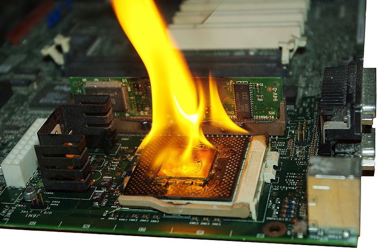 I also have no doubt that machine learning can be used effectively today for other tasks, such as research. However, we have a long way to go before we can trust an AI to offer advice that is as helpful as what you’d get from a human who has lived experience, judgment and empathy.
Note: As with all of our op-eds, the opinions expressed here belong to the writer alone and not Tom’s Hardware as a team.
Get instant access to breaking news, in-depth reviews and helpful tips.
Contact me with news and offers from other Future brandsReceive email from us on behalf of our trusted partners or sponsors
Avram Piltch is Tom’s Hardware’s editor-in-chief. When he’s not playing with the latest gadgets at work or putting on VR helmets at trade shows, you’ll find him rooting his phone, taking apart his PC or coding plugins. With his technical knowledge and passion for testing, Avram developed many real-world benchmarks, including our laptop battery test.
Apple Releases M2 Pro and M2 Max: 20 Percent Faster, Up to 19 GPU Cores
(Image credit: Apple)
Despite reports that M2 Pro and M2 Max-based products were delayed yet again, Apple today announced the launch of new MacBook Pros and Mac Minis using the new SoCs. The M2 Pro and M2 Max are more powerful versions of the M2 launched last year in the MacBook Air.
As Apple explains, the M2 Pro “scales up” the M2, giving customers 10 or 12 CPU cores and up to 19 GPU cores. The 12-core configuration has eight high-performance cores and four efficiency cores. For comparison, the M2 in the MacBook Air comes with an 8-core CPU and either an 8- or 10-core GPU. The M2 Pro can also be paired with up to 32GB of unified memory.
(Image credit: Apple)
Apple claims that the 12-core M2 Pro is up to 20 percent faster than the 10-core version of the M1 Pro in multi-threaded apps. With the new 19-core GPU (three more than the M1 Pro’s GPU), performance is up to 20 percent faster.
For a real-world example, Apple says that the 16-inch MacBook with the M2 Pro is 25 percent faster than its M1 Pro counterpart while compiling in Xcode. It’s also allegedly 2.5x faster than the legacy 16-inch MacBook Pro with an Intel Core i9 processor. In addition, image processing in Photoshop is reportedly 40 percent faster than the M1 Pro and 80 percent faster than the Core i9.
Swipe to scroll horizontally
|
M2 Pro |
M2 Pro Max |
|
|---|---|---|
|
Process Technology |
5-nanometer |
5-nanometer |
|
Number of Transistors |
40 billion |
69 billion |
|
CPU Cores |
10 or 12 cores |
12 cores |
|
GPU Cores |
16 or 19 cores |
19 or 38 cores |
|
Max LPDDR5 Memory |
32GB |
96GB |
|
Unified Memory Bandwidth |
200GB/s |
400GB/s |
|
Neural Engine |
16-core |
16-core |
The M2 Max is the flagship SoC and has the same 12-core CPU as the M2 Pro but doubles the maximum number of GPU cores to 38. Performance is further enhanced by doubling unified memory bandwidth to 400 GB/s compared to 200 GB/s for the M2 Pro. As a result, graphics performance is up to 30 percent faster than the preceding M1 Max. While the M2 Pro can be paired with a maximum of 32GB of memory, the M2 Max triples that figure to 96GB.
(Image credit: Apple)
The M2 Pro and M2 Max are built on a 5nm process node, packing 40 billion transistors and 67 billion transistors, respectively. The two chips also share a 16-core Neural Engine capable of executing nearly 16 trillion operations per second (a 40 percent uplift compared to the previous generation). Other features include an enhanced version of the Secure Enclave security platform and a beefed-up media engine.
The M2 Pro is available in refreshed versions of the Mac mini, 14-inch MacBook Pro and 16-inch MacBook Pro. The M2 Max is only available on the new MacBook Pros. All of the M2 Pro- and M2 Max-equipped Macs ship on January 24th.
Get instant access to breaking news, in-depth reviews and helpful tips.
Contact me with news and offers from other Future brandsReceive email from us on behalf of our trusted partners or sponsors
Brandon Hill is a senior editor at Tom’s Hardware. He has written about PC and Mac tech since the late 1990s with bylines at AnandTech, DailyTech, and Hot Hardware. When he is not consuming copious amounts of tech news, he can be found enjoying the NC mountains or the beach with his wife and two sons.
Topics
Notebooks
CPUs
company developed hardware emulators and launched Linux / Habr
At the ISC High Performance 2020 conference, the Slovak company Tachyum announced 128-core Prodigy processors, as well as an AI complex based on them.
Processors are planned to be used in large data centers, high-load platforms, AI systems and other areas where high performance is needed. The chip is very complex, both in itself and in production, so its development is not carried out at the fastest pace. But the company is doing what it can, and doing quite well. About what has already been achieved — under the cut. nine0005
What kind of processor is this?
Tachyum positions it as a chip for highly loaded systems. One of the main directions is the use of the processor in AI training systems. The fact is that ready-made scenarios do not need super-productive systems — a specialized chip from any of the manufacturers is enough. But training AI platforms, especially large-scale ones, is another matter, here you need machine resources and time for training.
The developers stated that their processor and infrastructure designed for this chip are able to provide the necessary resources. The supercomputer, which is based on Prodigy chips, is quite powerful — 125 Pflops per rack and 4 exaflops for a full complex, consisting of 32 racks 52U high. nine0003
Each processor provides up to 625 teraflops, which is approximately 2.5 teraflops per server. To ensure the operation of the system, a server-module of the company’s own design is used. The advantage of Tachyum chips and systems, according to its representatives, is not only in powerful chips and infrastructure, but also in lower power consumption and cost — not only of the systems themselves, but also of their operation.
As for the processors themselves, they stand out among their “colleagues” not only in the number of cores, but also in their architecture. It is universal, which makes it possible to use chips not only in the field of AI, but also in many other industries. nine0003
In one cycle, the processor performs two 512-bit multiply-add operations, 2 load operations and one store operation. The floating point unit supports both double, single and half precision according to IEEE standards. If necessary, support for 8-bit floating point data types can also be enabled.
It is worth talking about the details of the architecture. So, the processor is being developed using the 7nm process technology. The older version contains 128 cores with a frequency of up to 4 GHz each, 12 DDR5-4800 memory channels, 48 PCI Express 5.0 lanes and two 400GbE controllers. nine0003
There is also a 64-core version that contains an eight-lane DDR5 controller, a 64-lane PCI Express 5.0 controller, and two 400GbE network interfaces.
As for motherboards, there are two options:
- Full size with 4 processors for the HPC segment.
- Compact with 1 processor for high density modular systems.
Software on systems with new chips can run as x86, ARMv8, or RISC-V binaries. Unfortunately, the speed of work will be somewhat lower than in the case of running on the «native» architecture — the drop is from 25% to 40%. But you can also compile the sources for a new architecture, if the speed is critical. nine0003
We love to review the most interesting and controversial topics from the IT world on Habré.
If you want to keep abreast of news that are traditionally included in the top read, subscribe to our blog.
Stages of chip development
Hardware emulator
As mentioned above, preliminary information about the chips appeared back in 2020. But the project began to develop most actively already in 2021.
So, at the end of March, the company announced the readiness of a hardware emulator, which makes it possible to evaluate the capabilities and performance of the new processor. nine0003
The emulator is based on FPGA (Field-Programmable Gate Array) and I/O boards. The emulator’s motherboard includes four programmable dies that simulate the operation of eight Prodigy cores at once. I/O boards have been added to the prototype. The supplied prototype can already be installed in a 19″ rack. If you take several emulators, they can be connected to each other, simulating different processor configurations. 0004 No one doubts that the production of such high-tech products as processors requires a huge amount of resources. This is, first of all, money, time, help of professionals.
In July 2021, Tachyum was able to receive new funds from investors, as a result of which Tachyum’s capitalization tripled at once. Unfortunately, the company did not indicate the exact amount of funds received.
Nevertheless, after that, the company’s representatives announced the intensification of the development of processors and the beginning of work on a supercomputer based on Prodigy chips. nine0003
Running Linux on a Tachyum Prodigy prototype
Already in September, based on the FPGA prototype, Linux was launched. The company previously announced UEFI readiness for Prodigy, but now a prototype processor can provide full support for the operating system.
During the tests, the company was able to run the OS and a simple application, after which the system was turned off. It is clear that this is not God knows what, but the developers sought to show the performance of the prototype. The processor quietly handles interrupts and exceptions, switching modes and providing correct timings. There is a demonstration of the prototype. The video, unfortunately, is only available on the company’s website, it was not posted on YouTube. nine0003
Recently, the company announced that it plans to show the work of a number of services, applications and user sessions in the near future.
“Realizing a successful Linux boot just two months after the development of the FPGA IO motherboard prototype is a huge achievement, completing a milestone. Moving on to further debugging and testing, we look forward to running more «heavy» applications on the Prodigy prototype as early as next month, ”a company representative said. nine0003
By the way, Tachyum’s ultimate goal is to create a supercomputer or a whole system of their supercomputers capable of simulating the functioning of the human brain.
Hardware tabs in processors — myths and reality / Sudo Null IT News The threat of their presence in modern processors is very often almost the main leitmotif in justifying the need to use only the domestic component base in Russia. Moreover, often, some unfortunate experts who have worked to earn fame in the field of domestic microelectronics postulate the presence of undocumented features in foreign CPUs as a self-evident question. In this article, I would like to outline the general picture of what the situation is with the potential presence of hardware bugs in reality and how much this threat is a problem. nine0003
First, let’s define some definitions. We will call a hardware tab in the processor some hardware block in the processor, intentionally hidden from the user at the stage of creation (design, production) and hardwired into silicon, which can in certain cases (on command, at the appointed time) allow an action not authorized by the user (to give control to the processor , give access to data, disable the processor or change its characteristics). It is especially worth mentioning here that we are not talking about malicious system software or firmware that can be changed after the production of the processor (by the manufacturer of the end devices or simply by any user). Also, I will talk about hardware tabs in the CPU, and not in the final products built on their basis, such as computers, tablets, various industrial devices, component parts (for example, motherboards), etc. And one more important point — we will talk about industrial processors from well-known companies such as Intel, AMD, Qualcomm, etc., available on the mass market. For it is obvious that in a no-name processor from the NSA / FSB there can potentially be anything. nine0003
Let’s start with the main message of the entire article. In recent years, the topic of researching methods for injecting and detecting hardware bugs has become increasingly popular. Conferences are held, research groups publish articles of varying degrees of usefulness on methods for introducing bookmarks into processors. But in all this academic discussion, there is one fact that must be understood when reading published materials — over the decades of development of silicon microelectronics, NOT A SINGLE reliably proven hardware tab has been found in mass industrial processors . Thus, it can be stated that this threat is currently purely theoretical, but has not found (at least so far) its application in practice. Let’s try to figure out why this happens.
A modern microprocessor is an extremely complex engineering product that can contain several tens of billions of transistors (and not only transistors). In general, at first glance, it seems that with so many elements it is not difficult to add some circuits that can potentially perform actions hidden from the user. But the introduction of a bookmark has, roughly speaking, two aspects: technical and business. Let’s analyze them separately. nine0003
Technical aspects of the introduction of bugs
This is how the academic view of the problem of hardware trojans looks like:
Without delving into the taxonomy of hardware bugs, let’s consider the three most important for understanding the class of problems from the above diagram:
Types of bookmarks by activation mechanisms.
The result of unauthorized exposure.
Other details do not fundamentally affect the general understanding of the issue.
Let’s start with the last point — after all, it is for its implementation that all the others exist. To simplify the question, let’s take two possible options for triggering a hardware tab — processor failure and information leakage . By and large, the other options given (deterioration of characteristics and change in the behavior of the processor) are, in the limit, a processor failure, and for easier perception of the material, it is quite acceptable, I think, to reduce them to one point. nine0003
To simplify understanding, I would like to consider this issue with a slightly different approach than the authors of the above classification suggest.
Here, to begin with, it is worth recalling that the modern production of microprocessors is extremely globalized and has a large division of labor. There are companies developing processors, for example, from foreign ones: Intel, AMD, Nvidia, Qualcomm, MediaTek, etc., from domestic ones: Baikal Electronics, MCST, NIISI, Elvis, etc. But being directly responsible for the development, these companies involve many third-party enterprises in the production chain to create the final product. For example, all of the above companies directly manufacture most of their processors at TSMC factories in Taiwan (except for Intel, which also has its own production and orders only a small part of its processors from TSMC so far). Also, all companies use third-party software for designing processors, primarily from Synopsis and Cadence. Licensed IP blocks are massively used, somewhere more, somewhere less, but they are everywhere. Therefore, here it is worth dividing the question of the potential appearance of hardware tabs in the processor into two parts — when it appears by the intention of the developer directly, or when it appears hidden from the developer company due to the use of third-party companies in production or the results of their intellectual work
Implementation of the bookmark directly by the processor developer
There are no technical difficulties to add the logic that the creator wishes to the processor, this is obvious. But a problem arises — how then to use such a bookmark? As well as a variety of organizational complexities and consequences. We will talk about this a little lower.
The introduction of a bookmark by third parties in the production of the processor.
This option should be recognized as much more complicated (I would say almost unrealistic). It has all the same technical and organizational difficulties (and even more) as the previous paragraph, but with the only difference that it is much easier for the processor developer to control the occurrence of unauthorized changes. Any more or less complex circuit that suddenly appeared when compiling the source code of the project is unlikely to escape the vigilant eyes of engineers. A high degree of division of labor when creating a processor is also an obstacle to the introduction of bookmarks, because. in the general case, it does not give the attacker knowledge about the characteristics and features of the remaining links in production. For example, the creation of photomasks is usually separated from production at the factory, packaging is also carried out in other places, not to mention the fact that the introduction of any transistor at this stage without the knowledge of the developer can turn the chip into a brick. nine0003
But let’s assume that the malicious developer of the processor did decide to make a secret backdoor, no matter what motivated him to do so. Omitting organizational difficulties (more on them later), there are purely technical aspects that make such a decision rather meaningless.
Bookmarks can be roughly divided into 2 categories — requiring activation (by command from outside through various channels, or activated upon reaching a certain event, for example, by some internal counter) and constantly working
Bookmarks via activation.
In theory, the bookmark can be activated in various ways:
-
On the event of an internal counter (reaching a certain time, the number of times the power-on circuit has been triggered, etc.
). The problem with these bookmarks is obvious — they are not controlled. How can you predict how many times the computer will turn on, one or thousands? Or when you need to turn off the processor — in a year, two, or five years?
-
On command from outside. In this case, the question again arises — how to transfer the command to the desired processor? If a computer with a vulnerable processor is in a remote data center in an iron case and there are five more of the same racks above it, then the tab cannot be activated by any radio or optical signals. The only option left is to somehow send a complex sequence of commands through the network for execution to the processor, which will be a trigger for switching on. But in order to do this, you need to be able to directly run the code on the processor. The following cases are possible here:
-
The computer is not directly connected to the WAN. In this case, it will be impossible to activate the bookmark by running the desired sequence of commands — you simply will not physically reach the processor.
-
A server with a vulnerable processor is used to provide remote access for clients (for example, this is a virtual machine rental service). In this case, running the desired code is as easy as shelling pears — you rent a virtual machine and run the desired sequence of instructions in it. nine0003
-
A machine with a vulnerable processor has access to the global network and exposes certain services to the outside (but does not allow user code to run directly). In theory, one can imagine that by a certain impact on the service (for example, some special request), we can activate an extremely rarely working code branch in the software, which will contain the sequence necessary for activation. But here the problem is quite obvious — how to ensure that the machine we are interested in runs exactly the software stack that we need, up to its binary identity? During the creation of the processor, which can take several years, both the software stack itself and the versions of its components, libraries, compilers, etc.
can change. And the slightest change in all this software will lead to the meaninglessness of your hardware bookmark. And I’m not talking about all the delights of overcoming network equipment / stack, which can also introduce insurmountable obstacles. nine0003
-
Another variation for point 3 is possible — the machine with the service is hacked through a software vulnerability, and then the necessary code is launched on it. But in this case, the meaning of a hardware tab is practically lost — if you can hack a computer purely programmatically, why bother with hardware backdoors? Unless you activate a bookmark that will physically destroy the processor.
Bookmarks that work all the time
But let’s say we decided to bypass all the difficulties with activating the hardware bookmark and made it work right from the factory. Thus, immediately when you turn on your processor, it will start trying to transfer some information somewhere. The problem lies precisely in these «some» and «somewhere». The processor must somehow determine which of the entire array it processes is valuable information and where to send it. Even if we assume that not a single network administrator in the world will notice the constantly flashing incomprehensible traffic on his network, the problem is that at the level of implementation of the processor logic it is difficult to determine where and how to correctly send any data to the outside world. If the processor has a built-in Ethernet controller, then its hardware implementation (which, obviously, it makes sense to bookmark) must also make friends with the driver stack of the machine and the equipment used on the network. This can be a daunting task, to say the least. What if the user is using an external network card? To do this, you will have to somehow integrate into the work of the PCI interface and at the same time not break the work of an unknown network card and arbitrary drivers for it. Sounds almost unrealistic. But most importantly, even if all these difficulties are overcome, it is not clear how to overcome quite standard security settings on network equipment.
The network can be organized in different ways, you need to know the addresses of the gateways, and many settings are at the OSI levels above the channel on which the Ethernet adapter operates. Simply sending a packet with a silicon-hardened destination IP address on any minimally complex network will cause it to be rejected on the first network device. As a result, minimal efforts to properly organize the internal network make the network bookmark a meaningless set of transistors. Implementing such functionality in silicon that can intelligently bypass network security settings looks like science fiction
All of the above difficulties are also relevant for bookmarks with activation, in the event that we somehow managed to activate the malicious functionality and its purpose is to transfer information from the processor to the outside world
So which hardware bookmarks are realistic?
To sum up, a technically realistic situation is when the processor developer himself put a hardware tab into the processor and it can be activated using some special command sequence. You can use such a bookmark only if you can directly run the code on the processor of interest to us, which is relevant for virtual machine/server rental services. In this case, you can either access other people’s data or physically destroy the processor. Also, for machines that provide services to the global network, you can use a combination of software vulnerabilities and hardware tabs to destroy the processor physically. nine0003
All other options appear to be technically unrealizable.
Business aspects of the introduction of bugs
In addition to the technical ones, the deliberate introduction of bugs into chips has other aspects for the developer company, which we can roughly generalize under the term «business»:
-
Reputational losses — if it suddenly turns out that someone deliberately introduces bookmarks into their processors, this company will be bypassed by everyone who has the slightest opportunity for this
-
Risk of leakage of information about the mechanisms of operation of the hardware tab to third parties
The implementation of the hardware tab in the processor requires the involvement of company employees, and most likely in the amount of more than one person.
Each of them can then leak this information, for example, to criminal structures or intelligence agencies of other countries. As a result, there is a danger of unauthorized use of the backdoor
-
Legal
If the operation of the bookmark leads to data leaks, or, moreover, to man-made disasters, then the developer of such a chip will simply be destroyed in the courts. And I want to separately note that this issue cannot be resolved by any methods of organizing the supply of vulnerable chips only to the “necessary” countries. Because it is physically impossible to control the movement of all chips with millions of copies. And no one from RosAtom will give a guarantee that a processor with a stub will not end up at a nuclear power plant in India
-
Economic
Creating bookmarks requires additional financial costs. In the limit, this will require the creation of a separate line of processors, with the corresponding costs for the creation of individual photomasks and the production cycle as a whole.
This is an extremely expensive pleasure. Also, the introduction of any complex logic into the processor can lead to a deterioration in its performance, such as a decrease in frequency or an increase in power consumption. This also has economic implications. nine0003
What is the result?
Summarizing the above, we can say that the implementation of hardware tabs in the processor, on the one hand, has many risks and negative consequences for the developer, which can simply destroy any company. On the other hand, from a technical point of view, the introduction of a bookmark directly into the processor does not give the desired result — the use cases are extremely limited and are often easily countered by simple organizational measures. It is much easier and more efficient to implement bookmarks at the level of creating firmware, system software or final products (hardware, motherboards, etc.). That is why at the moment there is such a situation that, being theoretically possible for implementation, in practice, hardware bookmarks in processors have never been found. nine0003
Known misconceptions that are considered to be “hardware tabs in processors”
For completeness, I would like to go through the most exaggerated examples of “hardware tabs in processors” on the net, which, of course, are not such on closer examination:
-
Iranian centrifuges.
The story of the disabling of the Iranian nuclear facility has a trivial reason in the form of the introduction (intentional or not) of the Stuxnet 9 software virus0003
-
Intel ME, Intel AMT
Without going into arguments about how safe these technologies are, we can simply state that they are implemented on the basis of a separate processor on the motherboard and are not part of the CPU.
-
Snowden’s List
The exposé from a former CIA/NSA employee provides ample material for analyzing the methods used by US intelligence to obtain necessary information without the consent of users. But there are no hardware tabs in industrial processors.
nine0003
-
BMC on a Chinese board
Here we have a suspicion of insecure flash firmware of the BMC module.
-
VIA God Mode
This is quite an interesting case, which is closest to the hardware tab. The authors of an article published in 2018 even loudly called it “the first ever discovered backdoor in x86 processors.” Everything would be fine, but if the authors carefully read the documentation for VIA processors, they would find that the description of this “bookmark” has been there since 2004. Therefore, it cannot be called undocumented for sure. Yes, and its activation requires inclusion in the BIOS, which also does not allow it to be recognized as a hidden hardware tab. nine0003
Another indirect (but very weighty) evidence of the absence of hardware bugs in processors is the events that unfolded after February 24, 2022. After the start of the NWO in Ukraine, the level of confrontation between Russia and the US and the EU reached a critical level. In fact, the parties use almost all possible methods of causing damage, except for a direct military clash between the armies of states. This includes regular hacker attacks on the information infrastructure of Russia, which led to the collapse of some government services. But all this happened only with the use of software vulnerabilities. I think no one doubts that if there were hardware tabs in the Intel / AMD processors (on which the entire infrastructure of the country is built), they would be used. But we don’t see this. Moreover, an open secret is the fact that despite the mass of bravura statements for the press about the success of import substitution in critical industries, even in military equipment, a foreign component base has been and is still widely used. On this occasion, the US Department of Commerce even initiated a separate investigation. The British think tank RUSI published an interesting report with an analysis of the component base in the wreckage of missiles from Iskander-M and Tornado, and at the end gave a detailed list of foreign products in the Borisoglebsk-2 electronic warfare station captured in Ukraine.
And yet, we also do not observe any massive problems with the failure of military equipment due to the activation of bookmarks. nine0003
So why do we need domestic processors, if not to deal with bookmarks?
The problem of active exaggeration of scarecrows about hardware bugs is that, being nothing more than a marketing tool in unscrupulous hands, it generates false paths for the development of the domestic microelectronic industry. If our goal is to ensure security in terms of hardware bugs, then organizing the assembly of end products in Russia based on any components (including foreign ones) plus control over the security of the system software stack gives the desired result — there will be no hardware bugs in domestic computing systems and equipment. It may sound paradoxical, but in order to solve the problem of hardware tabs, the development of own processors, by and large, is not needed. nine0003
So why do we need domestic processors? At least for 2 quite obvious purposes:
-
Information security.