Page not found
Page not found
We couldn’t find such page: /en/video/geforce-rtx-2070-super-vs-geforce-rtx-2080-super%23general-info
Popular graphics cards comparisons
GeForce RTX
3060 Ti
vs
GeForce RTX
3060
GeForce RTX
2060 Super
vs
GeForce RTX
3060
GeForce GTX
1060 6 GB
vs
Radeon RX
580
GeForce RTX
3060 Ti
vs
GeForce RTX
3070
GeForce GTX
1660 Super
vs
GeForce RTX
3050 8 GB
GeForce GTX
1660 Super
vs
Radeon RX
580
Popular graphics cards
GeForce RTX
4090
Radeon RX
580
Radeon RX
Vega 7
GeForce GTX
1650
GeForce RTX
3060
GeForce GTX
1050 Ti
Popular CPU comparisons
Ryzen 5
5600X
vs
Core i5
12400F
Ryzen 5
3600
vs
Ryzen 5
5500
Core i5
10400F
vs
Core i3
12100F
Ryzen 5
3600
vs
Core i5
10400F
Ryzen 5
3600
vs
Core i3
12100F
Core i5
12400F
vs
Core i5
13400F
Popular CPUs
EPYC
9654
Ryzen 5
5500U
Core i3
1115G4
Core i5
12400F
Core i5
1135G7
Ryzen 5
3600
Page not found
Page not found
We couldn’t find such page: /en/video/geforce-rtx-2070-super-vs-geforce-rtx-2080-super%23benchmarks
Popular graphics cards comparisons
GeForce RTX
3060 Ti
vs
GeForce RTX
3060
GeForce RTX
2060 Super
vs
GeForce RTX
3060
GeForce GTX
1060 6 GB
vs
Radeon RX
580
GeForce RTX
3060 Ti
vs
GeForce RTX
3070
GeForce GTX
1660 Super
vs
GeForce RTX
3050 8 GB
GeForce GTX
1660 Super
vs
Radeon RX
580
Popular graphics cards
GeForce RTX
4090
Radeon RX
580
Radeon RX
Vega 7
GeForce GTX
1650
GeForce RTX
3060
GeForce GTX
1050 Ti
Popular CPU comparisons
Ryzen 5
5600X
vs
Core i5
12400F
Ryzen 5
3600
vs
Ryzen 5
5500
Core i5
10400F
vs
Core i3
12100F
Ryzen 5
3600
vs
Core i5
10400F
Ryzen 5
3600
vs
Core i3
12100F
Core i5
12400F
vs
Core i5
13400F
Popular CPUs
EPYC
9654
Ryzen 5
5500U
Core i3
1115G4
Core i5
12400F
Core i5
1135G7
Ryzen 5
3600
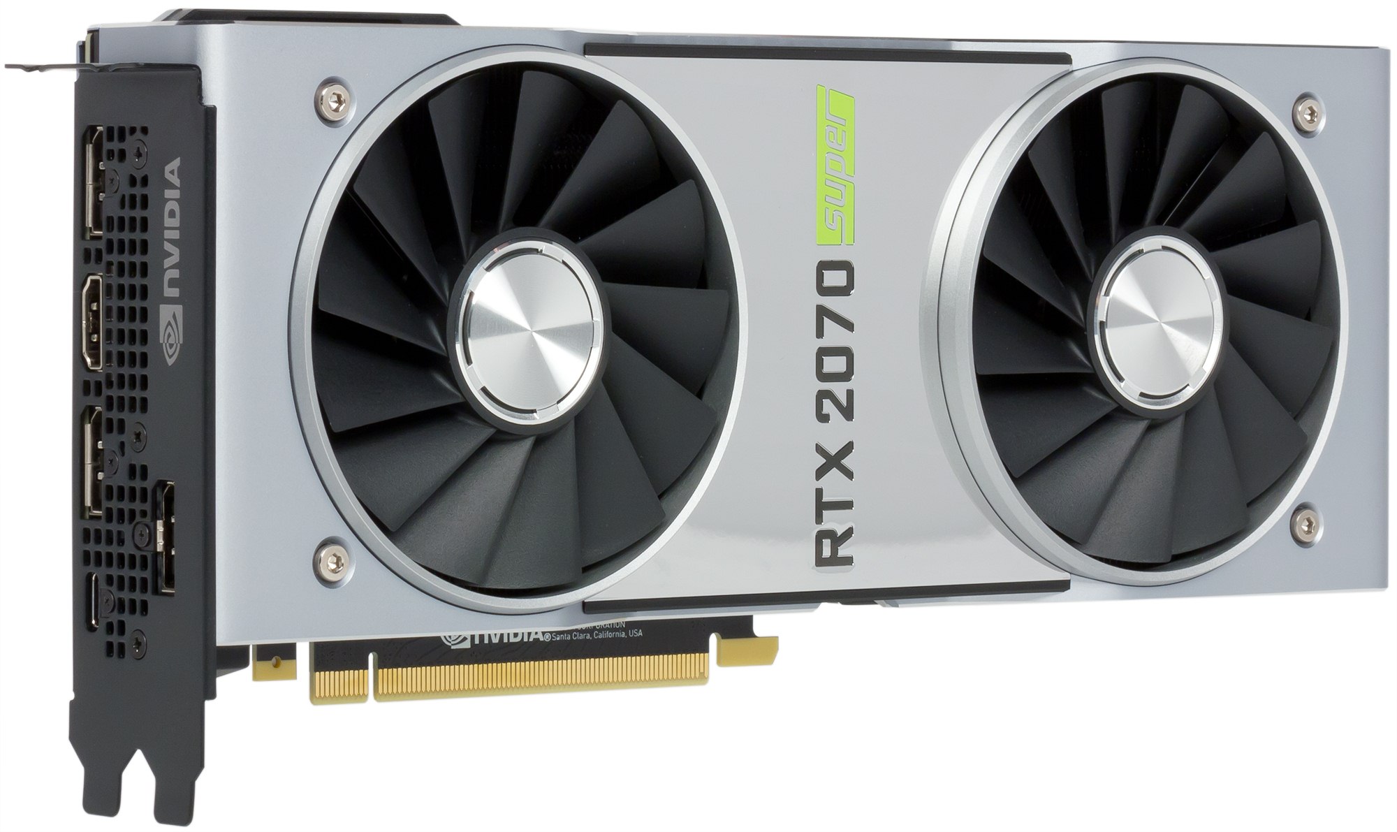
NVIDIA GeForce RTX 2070 Super vs NVIDIA GeForce RTX 2080 Super
NVIDIA GeForce RTX 2070 Super
NVIDIA GeForce RTX 2080 Super
GPU base clock
Graphic processing unit (GPU) is characterized by high clock frequency.
1605MHz
max 2457
Average: 1124.9 MHz
1650MHz
max 2457
Average: 1124.9 MHz
GPU memory frequency
This is an important aspect calculating memory bandwidth
1750MHz
max 16000
Average: 1468 MHz
1937 MHz
max 16000
Average: 1468 MHz
FLOPS
The measurement of processing power of a processor is called FLOPS.
9.28TFLOPS
max 1142.32
Average: 53 TFLOPS
11.19 TFLOPS
max 1142.32
Average: 53 TFLOPS
RAM
RAM in graphics cards (also known as video memory or VRAM) is a special type of memory used by a graphics card to store graphics data. It serves as a temporary buffer for textures, shaders, geometry, and other graphics resources that are needed to display images on the screen. More RAM allows the graphics card to work with more data and handle more complex graphic scenes with high resolution and detail.
Show all
8GB
max 128
Average: 4.6 GB
8GB
max 128
Average: 4.6 GB
Number of PCIe lanes
The number of PCIe lanes in graphics cards determines the speed and bandwidth of data transfer between the graphics card and other computer components through the PCIe interface. The more PCIe lanes a video card has, the more bandwidth and ability to communicate with other computer components.
Show all
16
16
L1 cache size
L1 cache size in video cards is usually small, measured in kilobytes (KB) or megabytes (MB). It is designed to temporarily store the most active and frequently used data and instructions, allowing the graphics card to access them faster and reduce delays in graphics operations.
64
64
Pixel draw speed
The higher the pixel rendering speed, the smoother and more realistic the graphics and movement of objects on the screen will be.
Show all
113 GTexel/s
max 563
Average: 94.3Gtexel/s
116 GTexel/s
max 563
Average: 94.3Gtexel/s
TMUs
Responsible for texturing objects in 3D graphics. TMU provides textures to the surfaces of objects, which gives them a realistic look and detail. The number of TMUs in a video card determines its ability to process textures. The more TMUs, the more textures can be processed at the same time, which contributes to better texturing of objects and increases the realism of graphics.
Show all
160
max 880
Average: 140.1
192
max 880
Average: 140.1
ROPs
Responsible for the final processing of pixels and their display on the screen. ROPs perform various operations on pixels, such as blending colors, applying transparency, and writing to the framebuffer. The number of ROPs in a video card affects its ability to process and display graphics. The more ROPs, the more pixels and image fragments can be processed and displayed on the screen at the same time. A higher number of ROPs generally results in faster and more efficient graphics rendering and better performance in games and graphics applications.
Show all
64
max 256
Average: 56.8
64
max 256
Average: 56.8
Number of shading blocks
The number of shader blocks in video cards refers to the number of parallel processors that perform computational operations in the GPU. The more shader units in the video card, the more computing resources are available for processing graphics tasks.
Show all
2560
max 17408
Mean value:
3072
max 17408
Mean value:
L2 cache size
Used to temporarily store data and instructions used by the video card when performing graphics calculations.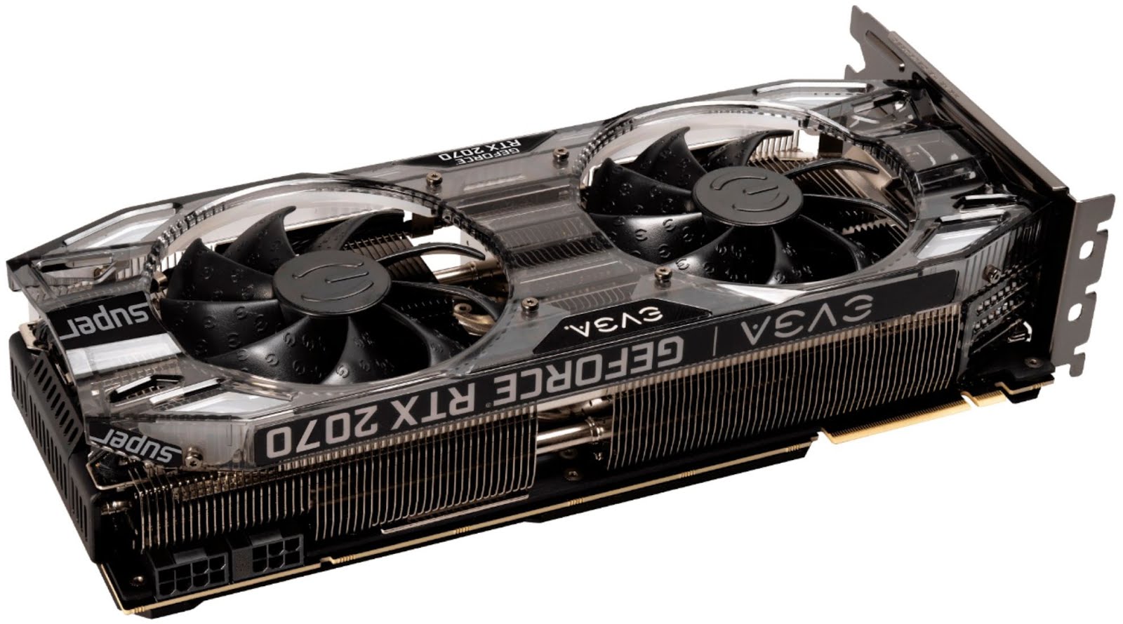 A larger L2 cache allows the graphics card to store more data and instructions, which helps speed up the processing of graphics operations.
Show all
4000
4000
Turbo GPU
If the GPU speed drops below its limit, it can switch to a high clock speed to improve performance.
Show all
1770MHz
max 2903
Average: 1514 MHz
1815MHz
max 2903
Average: 1514 MHz
Texture size
A certain number of textured pixels are displayed on the screen every second.
Show all
283.2 GTexels/s
max 756.8
Average: 145.4 GTexels/s
348.5 GTexels/s
max 756.8
Average: 145.4 GTexels/s
Architecture name
Turing
Turing
GPU name
TU104
TU104
Memory bandwidth
This is the rate at which the device stores or reads information.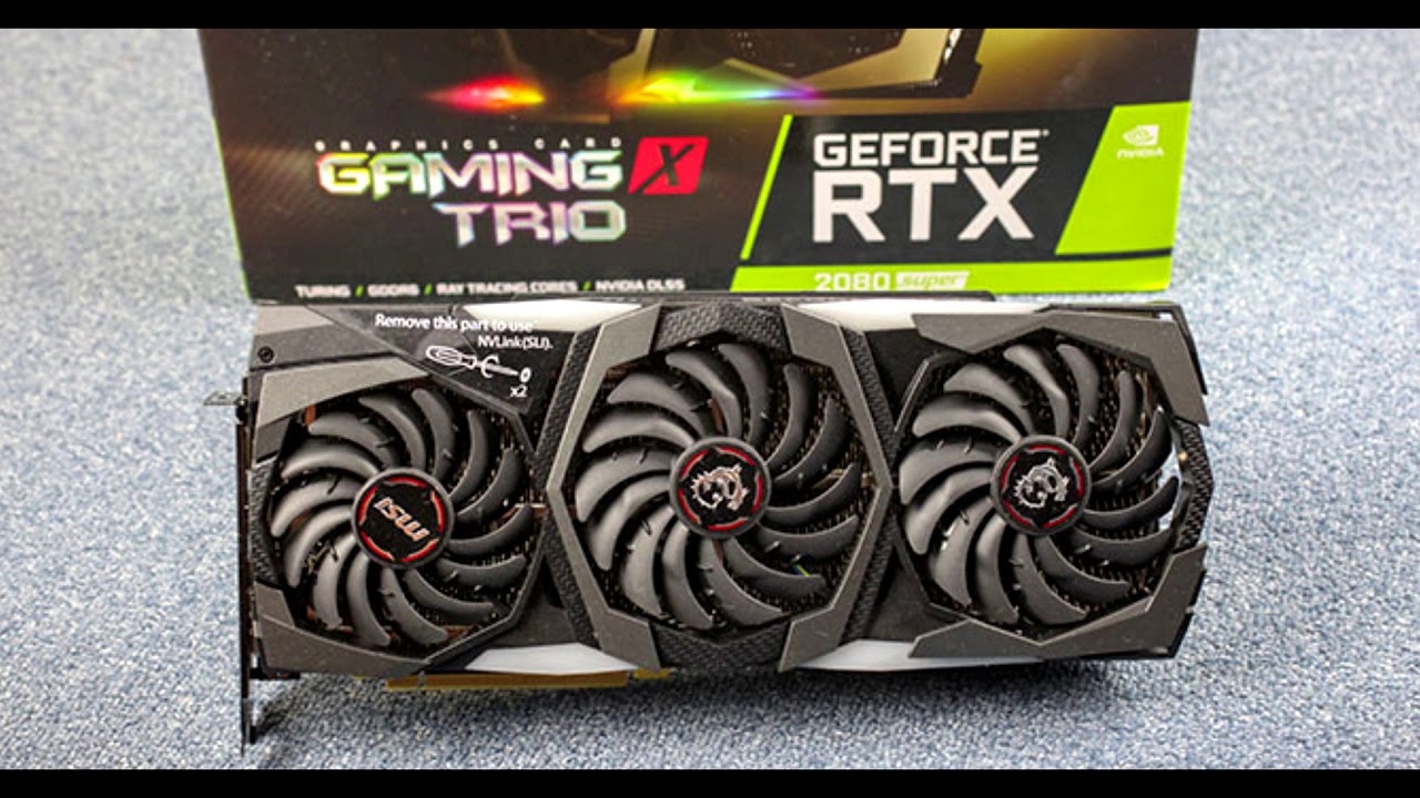
448GB/s
max 2656
Average: 257.8 GB/s
495.9GB/s
max 2656
Average: 257.8 GB/s
Effective memory speed
The effective memory clock speed is calculated from the size and information transfer rate of the memory. The performance of the device in applications depends on the clock frequency. The higher it is, the better.
Show all
14000MHz
max 19500
Average: 6984.5 MHz
15496MHz
max 19500
Average: 6984.5 MHz
RAM
RAM in graphics cards (also known as video memory or VRAM) is a special type of memory used by a graphics card to store graphics data. It serves as a temporary buffer for textures, shaders, geometry, and other graphics resources that are needed to display images on the screen. More RAM allows the graphics card to work with more data and handle more complex graphic scenes with high resolution and detail.
Show all
8GB
max 128
Average: 4.6 GB
8GB
max 128
Average: 4.6 GB
GDDR Memory Versions
Latest GDDR memory versions provide high data transfer rates to improve overall performance
Show all
6
Mean: 4.9
6
Mean: 4.9
Memory bus width
A wide memory bus indicates that it can transfer more information in one cycle. This property affects the performance of the memory as well as the overall performance of the device’s graphics card.
Show all
256bit
max 8192
Average: 283.9bit
256bit
max 8192
Average: 283.9bit
Crystal size
The physical dimensions of the chip that houses the transistors, microcircuits, and other components necessary for the operation of the video card. The larger the chip size, the more space the GPU takes up on the video card. Larger die sizes can provide more computing resources, such as CUDA cores or tensor cores, which can lead to increased performance and graphics processing capabilities.
Show all
545
max 826
Average: 356.7
545
max 826
Average: 356.7
Length
268
max 524
Average: 250.2
267
max 524
Average: 250.2
Generation
A new generation of graphics card usually includes improved architecture, higher performance, more energy efficient use, improved graphics capabilities and new features.
Show all
GeForce 20
GeForce 20
Manufacturer
TSMC
TSMC
Power supply capacity
90 002 When choosing a power supply for a video card, you must take into account the power requirements of the video card manufacturer, as well as other computer components.
Show all
550
max 1300
Mean value:
600
max 1300
Mean value:
Year of manufacture
2019
max 2023
Mean value:
2019
max 2023
Mean value:
Heat dissipation (TDP)
Heat dissipation requirement (TDP) is the maximum amount of energy that can be dissipated by the cooling system. The lower the TDP, the less power will be consumed.
Show in full
215W
Average value: 160 W
250W
Average value: 160 W
Process technology
The small size of the semiconductor means it is a new generation chip.
12 nm
Average: 34.7 nm
12 nm
Average: 34.7 nm
Number of transistors
The higher the number, the more powerful the processor is
13600 million
max 80000
Average: 7150 million
13600 million
max 80000
Average: 7150 million
PCIe version
Considerable speed is provided by the expansion card used to connect the computer to peripherals. The updated versions have impressive throughput and provide high performance.
Show all
3
Average: 3
3
Average: 3
Width
117mm
max 421.7
Average: 192.1mm
118mm
max 421.7
Average: 192.1mm
Height
34mm
max 620
Average: 89.6mm
34mm
max 620
Average: 89.6mm
Purpose
Desktop
Desktop
Sales start date
2019-07-02 00:00:00
9000 2 2019-07-02 00:00:00
Release price
$499
max 419999
Average: $5679.5
$699
max 419999
Average: $5679.5
OpenGL version
OpenGL provides access to the graphics card’s hardware capabilities for displaying 2D and 3D graphics objects. New versions of OpenGL may include support for new graphical effects, performance optimizations, bug fixes, and other improvements.
Show all
4.6
Mean value:
4.6
Mean value:
DirectX
Used in demanding games, providing enhanced graphics
12.2
max 12.2
Mean: 11.4
12.2
max 12.2
Mean: 11.4
Shader model version
The higher the shader model version in the video card, the more functions and possibilities are available for programming graphic effects.
Show all
6.6
max 6.7
Average: 5.9
6.6
max 6.7
Average: 5.9
Vulkan version
A higher Vulkan version usually means a larger set of features, optimizations, and improvements that software developers can use to create faster and more realistic graphical applications and games.
Show all
1.3
max 1.3
Mean value:
1.3
max 1.3
Mean value:
CUDA version
Enables the use of graphics card compute cores to perform parallel computations, which can be useful in areas such as scientific research, deep learning, image processing, and other computationally intensive tasks.
Show all
7.5
max 9.0
Mean value:
7.5
max 9.0
Mean value:
HDMI output
HDMI output allows you to connect devices with HDMI or mini HDMI ports. They can transmit video and audio to the display.
Yes
Yes
HDMI version
The latest version provides a wide signal transmission channel due to the increased number of audio channels, frames per second, etc.
Show all
2
max 2.1
Mean: 1.9
2
max 2. 1
1
Mean: 1.9
DisplayPort
Allows connection to a display using DisplayPort
3
Average: 2.2
3
Average: 2.2
Number of HDMI sockets
The more there are, the more devices can be connected at the same time (for example, game/TV type consoles)
Show all
1
Average: 1.1
1
Average: 1.1
USB Type-C
The device has a USB Type-C with a reversible connector orientation.
Yes
Yes
Interface 3 HDMI
A digital interface used to transmit high-definition audio and video signals.
Show all
Yes
Yes
Passmark Test Score
The Passmark Video Card Test is a program for measuring and comparing graphics system performance. It conducts various tests and calculations to evaluate the speed and performance of a graphics card in various areas.
Show all
17266
max 30117
Average: 7628.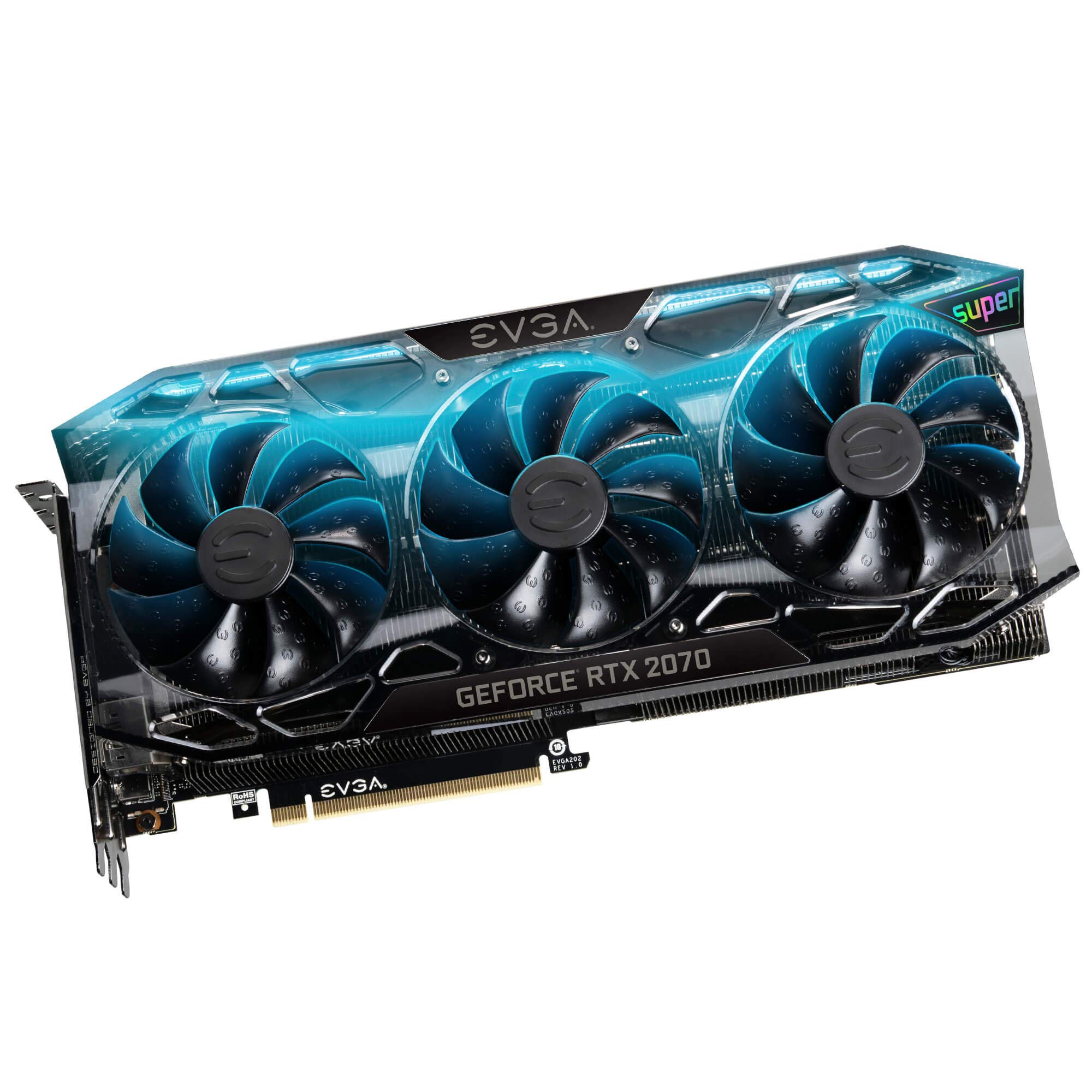 6
6
19579
max 30117
Average: 7628.6
3DMark Cloud Gate GPU test score
122452
max 196940
Average: 80042.3
140882
max 196940
Average: 80042.3
3DMark Fire Strike Score
20406
max 39424
Average: 12463
23447
max 39424
Average: 12463
3DMark Fire Strike Graphics Test Score
It measures and compares a graphics card’s ability to handle high-resolution 3D graphics with various graphic effects. The Fire Strike Graphics test includes complex scenes, lighting, shadows, particles, reflections, and other graphical effects to evaluate the graphics card’s performance in gaming and other demanding graphics scenarios.
Show all
23263
max 51062
Average: 11859.1
27494
max 51062
Average: 11859. 1
1
3DMark 11 Performance GPU score
31997
max 59675
Average: 18799.9
40550
max 59675
Average: 18799.9
3DMark Vantage Performance Score
65706
max 97329
Average: 37830.6
max 97329
Average: 37830.6
3DMark Ice Storm GPU score
478763
max 539757
Average: 372425.7
517703
max 539757
Average: 372425.7
SPECviewperf 12 test score — Solidworks
69
max 203
Average: 62.4
max 203
Average: 62.4
SPECviewperf 12 test score — specvp12 sw-03
The sw-03 test involves rendering and modeling objects using various graphic effects and techniques such as shadows, lighting, reflections and others.
Show all
67
max 203
Average: 64
72
max 203
Average: 64
SPECviewperf 12 test evaluation — Siemens NX
12
max 213
Average: 14
max 213
Average: 14
SPECviewperf 12 Test Evaluation — specvp12 showcase-01
The showcase-01 test is a scene with complex 3D models and effects that demonstrates the capabilities of the graphics system in processing complex scenes.
Show all
120
max 239
Average: 121.3
141
max 239
Average: 121.3
SPECviewperf 12 test score — Showcase
121
max 180
Average: 108.4
144
max 180
Average: 108.4
SPECviewperf 12 test evaluation — Medical
40
max 107
Average: 39. 6
6
max 107
Average: 39.6
SPECviewperf 12 test score — specvp12 mediacal-01
40
max 107
Average: 39
42
max 107
Average: 39
SPECviewperf 12 test score — Maya
143
max 182
Average: 129.8
135
max 182
Average: 129.8
SPECviewperf 12 test score — specvp12 maya-04
151
max 185
Average: 132.8
132
max 185
Average: 132.8
SPECviewperf 12 — Energy score
12
max 25
Average: 9.7
max 25
Average: 9.7
SPECviewperf 12 test score — specvp12 energy-01
12
max 21
Average: 10.7
12
max 21
Average: 10. 7
7
SPECviewperf 12 test score — Creo
48
max 154
Average: 49.5
max 154
Average: 49.5
SPECviewperf 12 test score — specvp12 creo-01
49
max 154
Average: 52.5
53
max 154
Average: 52.5
SPECviewperf 12 test score — specvp12 catia-04
94
max 190
Average: 91.5
108
max 190
Average: 91.5
SPECviewperf 12 evaluation — Catia
93
max 190
Average: 88.6
max 190
Average: 88.6
SPECviewperf 12 test score — specvp12 3dsmax-05
201
max 325
Average: 189.5
222
max 325
Average: 189.5
SPECviewperf 12 test score — 3ds Max
198
max 275
Average: 169. 8
8
228
max 275
Average: 169.8
Test and Review: GeForce RTX 2060 Super and RTX 2070 Super — New Versions of Graphics Cards
The game of hide and seek is over, NVIDIA has announced new graphics cards designed to compete with the AMD Radeon RX 5700 line, which will be officially released on July 7th. Namely, Super video cards. Not all rumors turned out to be true, NVIDIA didn’t just increase the clock speeds. You will learn all the performance details in the article.
According to rumors, NVIDIA has been preparing the Super line for quite some time, but was waiting for the right moment. Namely, the competitor’s move — AMD Radeon RX 5700 video cards based on the RDNA architecture, the prices of which are already known. However, on the technical specifications, NVIDIA did not have much flexibility, since the GPUs were shipped to partners a few weeks ago. But there were maneuvers in terms of price and final characteristics.
There were some delays. NVIDIA expected to receive the full technical specifications and prices of rival Radeon at Computex at the end of May. But AMD only announced new products without details, and the details appeared already at E3 two weeks later. So NVIDIA had to postpone Super graphics cards. At E3, AMD revealed the specs, and as a result, NVIDIA revealed some details about the upcoming Super. When the release date for AMD Ryzen processors and Navi graphics cards (July 7) became known, NVIDIA decided that the time had come. And sent two out of three video cards to the test labs, ahead of AMD.
NVIDIA has changed its positioning with Super graphics cards. Founders Editions models are no longer equipped with special A-GPUs and regular A-GPUs, which are also shipped to partners. Differences in the type of chips are a thing of the past. FE graphics cards are now the base for every line. So the partners will certainly introduce faster video cards, but slower options are not to be expected.
This review is for the GeForce RTX 2060 Super and GeForce RTX 2070 Super, both Founders Edition. First, we will look at the technical specifications, and then each video card in detail. If you’re interested in the details of the Turing architecture, we recommend checking out our theoretical overview of RTX, ray tracing, and new shader features.
| Model | GeForce RTX 2060 FE | GeForce RTX 2060 Super FE |
| Price | 31.990 ₽ 369 euro |
32.990 ₽ 419 euro |
| Technical specifications | ||
|---|---|---|
| Architecture | Turing | Turing |
| GPU | TU106-200 | TU106-410 |
| Process | TSMC 12 nm | TSMC 12 nm |
| Number of transistors | 10.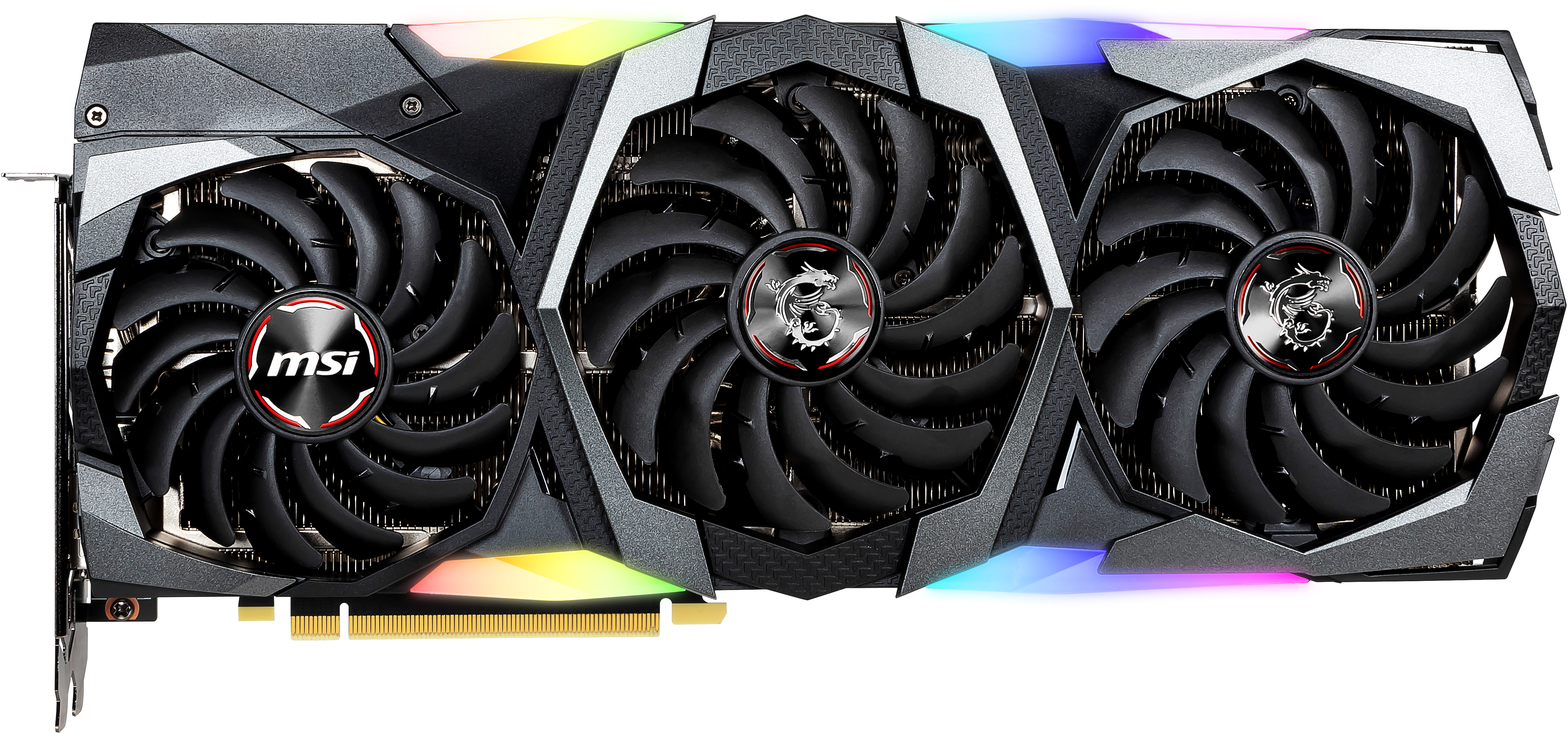 8 billion 8 billion |
10.8 billion |
| Crystal area | 445 mm² | 445 mm² |
| Stream Processors | 1.920 | 2.176 |
| Tensor cores | 240 | 272 |
| RT cores | 30 | 34 |
| Texture blocks | 120 | 136 |
| Geometric blocks | 15 | 17 |
| ROPs | 42 | 64 |
| GPU clock (base) | 1.365 MHz | 1.470 MHz |
| GPU clock (Boost) | 1.680 MHz | 1.650 MHz |
| Gigabeams/s | 5 PM/s | 6 PM/s |
| Memory frequency | 1.750 MHz | 1.750 MHz |
| Memory type | GDDR6 | GDDR6 |
| Memory size | 6GB | 8GB |
| Memory bus width | 192 bits | 256 bits |
| Capacity | 336 GB/s | 448 GB/s |
| TGP | 160 W | 175 W |
Add. nutrition nutrition |
1x 8-pin | 1x 8-pin |
GeForce RTX 2060 Super opens the list of new Super graphics cards «from the bottom», here the biggest changes have taken place. The TU106-410 GPU is now used instead of the TU106-200. There are 3 Graphics Processing Clusters (GPC) clusters and 17 Texture Processing Clusters (TPC) clusters on the chip. That gives 34 streaming multiprocessors (SMs) or 2,176 stream processors, 64 on each SM. The GPU also offers 272 Tensor cores (eight per SM) and 34 RT cores (one per SM). Note also 136 texture units. The L2 cache size is 4 MB.
NVIDIA has used a different level of GPU expansion for the GeForce RTX 2060 Super, now we are getting more stream processors and other GPU hardware units. The memory interface has also changed. Instead of 6 GB of GDDR5 over a 192-bit interface, the Super version is equipped with 8 GB over a 256-bit interface, more familiar to the Turing architecture. With a clock speed of 1. 750 MHz, we get a memory bandwidth of 448 GB/s.
The clock frequencies have also increased: in the case of the base frequency, we got an increase from 1.365 to 1.470 MHz. But the guaranteed Boost frequency has decreased a bit — from 1.680 to 1.650 MHz. NVIDIA increased the TGP from 160W to 175W due to the larger GPU and more memory. But the 8-pin socket is still sufficient for additional power for the Founders Edition.
| Model | GeForce RTX 2070 FE | GeForce RTX 2070 Super FE |
| Price | 48.990 ₽ 639 euro |
39.990 ₽ 529 euro |
| Technical specifications | ||
|---|---|---|
| Architecture | Turing | Turing |
| GPU | TU106-400 | TU104-410 |
| Process | TSMC 12 nm | TSMC 12 nm |
| Number of transistors | 10. 8 billion 8 billion |
13.6 billion |
| Crystal area | 445 mm² | 545 mm² |
| Stream Processors | 2.304 | 2.560 |
| Tensor cores | 288 | 320 |
| RT cores | 36 | 40 |
| Texture blocks | 144 | 160 |
| ROPs | 64 | 64 |
| GPU clock (base) | 1.410 MHz | 1.605 MHz |
| GPU clock (Boost) | 1.710 MHz | 1.770 MHz |
| Gigabeams/s | 6 MW/s | 7 MW/s |
| Memory frequency | 1.750 MHz | 1.750 MHz |
| Memory type | GDDR6 | GDDR6 |
| Memory size | 8GB | 8GB |
| Memory bus width | 256 bit | 256 bit |
| Capacity | 448 GB/s | 448 GB/s |
| TGP | 185 W | 215 W |
Add. nutrition nutrition |
1x 8-pin | 1x 8-pin 1x 6-pin |
NVIDIA has also changed the GPU type of the GeForce RTX 2070 Super. Instead of the TU106-400, the TU104-410 is now used, which was previously found in this form with the GeForce RTX 2080. Five or six Graphics Processing Clusters (GPCs) are used on the chip. Let’s note 20 TPC clusters, that is, 40 streaming multiprocessors (SMs). We ended up with 2.560 stream processors (40 x 64 = 2.560). Tensor and RT cores are available on die — 320 Tensor cores and 40 RT cores. Note also 184 texture units. The L2 cache is 4 MB in size.
8 GB of GDDR6 memory is connected on a 256-bit bus, which gives a bandwidth of 448 GB / s, no change here. The base frequency has increased from 1.410 to 1.605 MHz, the Boost frequency has increased from 1.710 to 1.770 MHz. However, in practice, the clock frequency should be higher. The power consumption of the Total Graphics Power graphics card has increased from 185 to 215 watts.
At E3, we got our first look at the GeForce RTX 2080 Super Founders Edition. The video card was also announced today, but technical details will come later. NVIDIA is going to sell this model from July 23rd.
| Model | GeForce RTX 2080 FE | GeForce RTX 2080 Super FE |
| Price | 63.990 ₽ 849 euro |
56.990 ₽ 739 euro |
| Technical specifications | ||
|---|---|---|
| Architecture | Turing | Turing |
| GPU | TU104-400 | TU104-450 |
| Process | TSMC 12 nm | TSMC 12 nm |
| Number of transistors | 13.6 billion | 13.6 billion |
| Crystal area | 545 mm² | 545 mm² |
| Stream Processors | 2.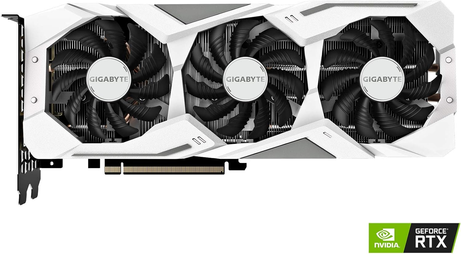 944 944 |
3.072 |
| Tensor cores | 368 | 384 |
| RT cores | 46 | 48 |
| Texture blocks | 184 | 192 |
| ROPs | 64 | 64 |
| GPU clock (base) | 1.515 MHz | 1.650 MHz |
| GPU clock (Boost) | 1.800 MHz | 1.815 MHz |
| Memory frequency | 1.750 MHz | 1.938 MHz |
| Memory type | GDDR6 | GDDR6 |
| Memory size | 8GB | 8GB |
| Memory bus width | 256 bit | 256 bit |
| Capacity | 448 GB/s | 496.1 GB/s |
| TGP | 225W | 250W |
GeForce RTX 2060 Super is based on six GPC (graphics processing cluster), 24 TPC (texture processing cluster) clusters and 48 streaming multiprocessors (SM).