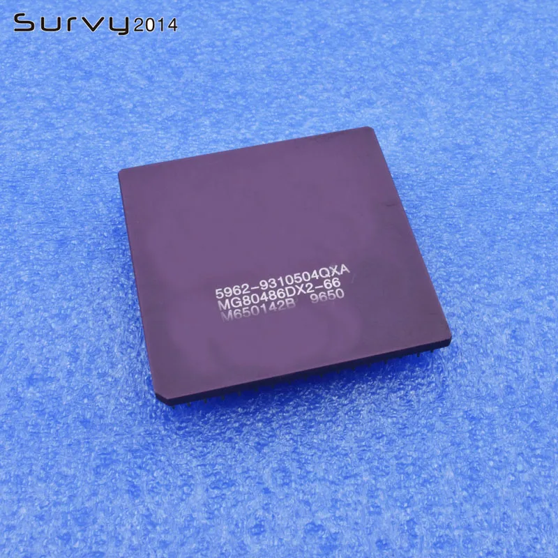
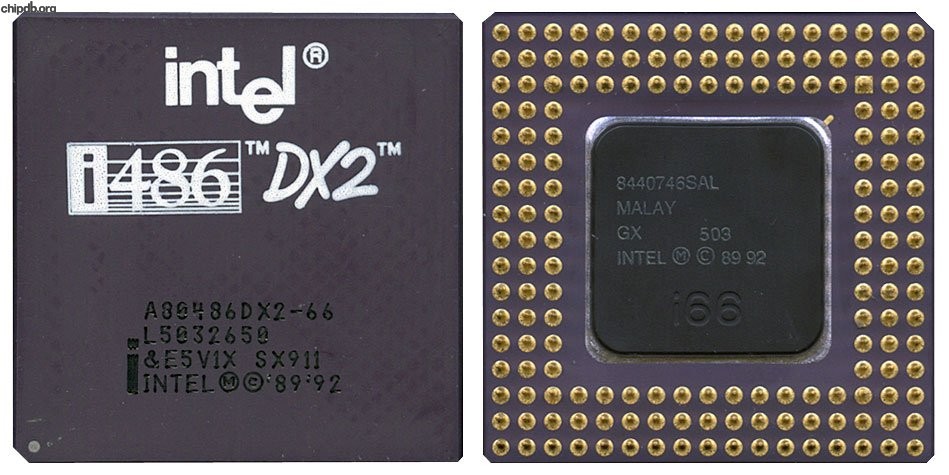
80486 — Intel — WikiChip
| Intel 80486 | |
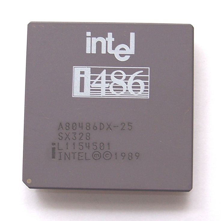
| Intel A80486DX-25 | |
| Developer | Intel |
| Manufacturer | Intel |
| Type | Microprocessors |
| Introduction | April 10, 1989 (announced) June, 1989 (launch) |
| Production | 1988-2007 |
| Architecture | x86 |
| ISA | IA-32 |
| µarch | 80486 |
| Word size | 32 bit
4 octets |
| Process | 1 µm
1,000 nm , 800 nm 0.8 μm , 600 nm 0.6 μm |
| Technology | CMOS |
| Clock | 16 MHz-100 MHz |
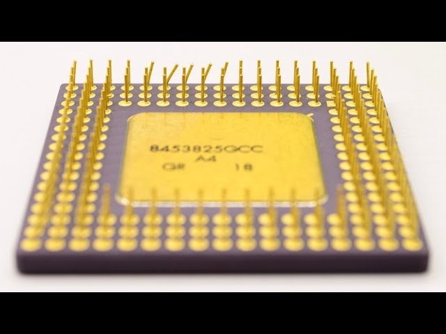
| Package | PGA-168, PQFP-196, SQFP-208 |
| Succession | |
| ← | → |
| 80386 | Pentium |
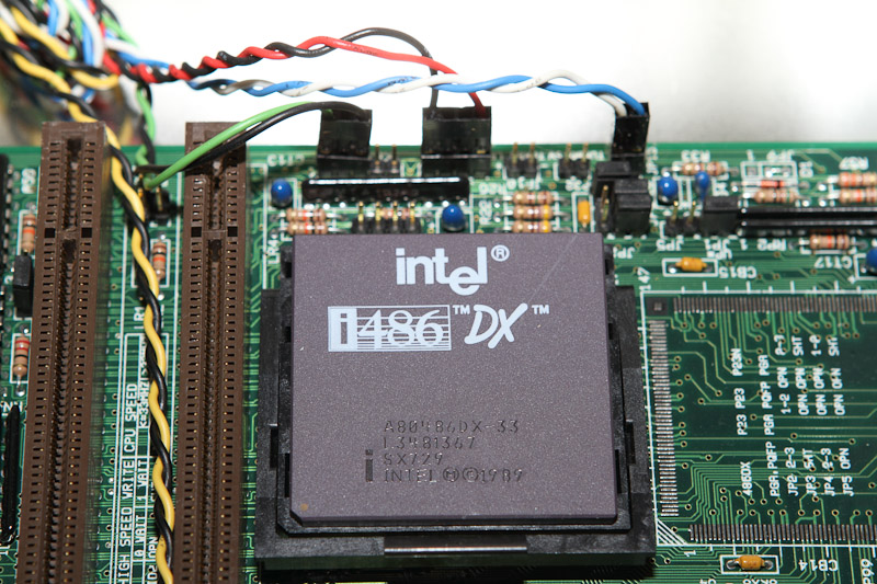
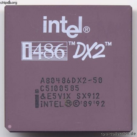
The 80486, also i486 and 486, (pronounced eighty-four-eighty-six) was a family of 32-bit 4th-generation x86 microprocessors introduced by Intel in 1989 as a successor to the 80386. 486 introduced a number of enhancements to 386 including a new level 1 cache, better IPC performance, and an integrated FPU. The 486 became the first x86 chip family to exceed one million transistors.
Contents
- 1 Architecture
- 2 Members
- 2.1 i486DX
- 2.2 i486SX
- 2.3 i486SL
- 2.4 i486GX
- 3 Clones
- 4 Documents
- 4.1 Datasheet
- 4.2 Manual
Architecture[edit]
- Main article: 80486 Microarchitectures
Like its predecessor, the 80486 maintains full backwards object code comparability with the all previous x86 processors (80386, 80286, 80186, etc…). To improve performance Intel introduced a new layer of cache on-die (previously various external extensions existed). The 8 KB, 4-way set associative, write-back policy, cache was unified for both the data and instructions. This provided much needed faster access to recently used data and instructions. Various enhancements were also made to the bus interface including faster communication that required single clock cycle instead of multiple.
Whereas before a separately packaged math coprocessor was used (i.e. 80387, 80287, etc..), the 80486 moved the unit on-die eliminating the external communication delays altogether. Furthermore more aggressive math algorithms were used to implement the new FPU yielding faster floating point calculations.
The pipeline itself received some attention as well. Simple ALU register, register and register, immediate cached operations could now complete in a single cycle; this previously required at least 2 cycles.
Members[edit]
i486DX[edit]
| i486DX Processors | |||||||||||||||
|---|---|---|---|---|---|---|---|---|---|---|---|---|---|---|---|
| Model | Launched | Process | Freq | Max Mem | |||||||||||
| i486DX-20 | June 1989 | 1,000 nm
1 μm 800 nm 0.8 μm |
20 MHz
0. |
4,096 MiB
4,194,304 KiB |
|||||||||||
| i486DX-25 | June 1989 | 1,000 nm
1 μm 800 nm 0.8 μm |
25 MHz
0.025 GHz |
4,096 MiB
4,194,304 KiB |
|||||||||||
| i486DX-33 | 7 May 1990 | 1,000 nm
1 μm 800 nm 0.8 μm |
33 MHz
0.033 GHz |
4,096 MiB
4,194,304 KiB |
|||||||||||
| i486DX-50 | 24 June 1991 | 1,000 nm
1 μm 800 nm 0.8 μm |
50 MHz
0.05 GHz |
4,096 MiB
4,194,304 KiB |
|||||||||||
| i486DX2-40 | 3 March 1992 | 1,000 nm
1 μm 800 nm 0.8 μm |
40 MHz
0.04 GHz |
4,096 MiB
4,194,304 KiB |
|||||||||||
| i486DX2-50 | 3 March 1992 | 1,000 nm
1 μm 800 nm 0.8 μm |
50 MHz
0.05 GHz |
4,096 MiB
4,194,304 KiB |
|||||||||||
| i486DX2-66 | 3 March 1992 | 1,000 nm
1 μm 800 nm 0.8 μm |
66 MHz
0.066 GHz |
4,096 MiB
4,194,304 KiB |
|||||||||||
| i486DX4-100 | 7 March 1994 | 600 nm
0.6 μm |
100 MHz
0.1 GHz |
4,096 MiB
4,194,304 KiB |
|||||||||||
| i486DX4-75 | 7 March 1994 | 600 nm
0. |
75 MHz
0.075 GHz |
4,096 MiB
4,194,304 KiB |
|||||||||||
| Count: 9 | |||||||||||||||
 02 GHz
 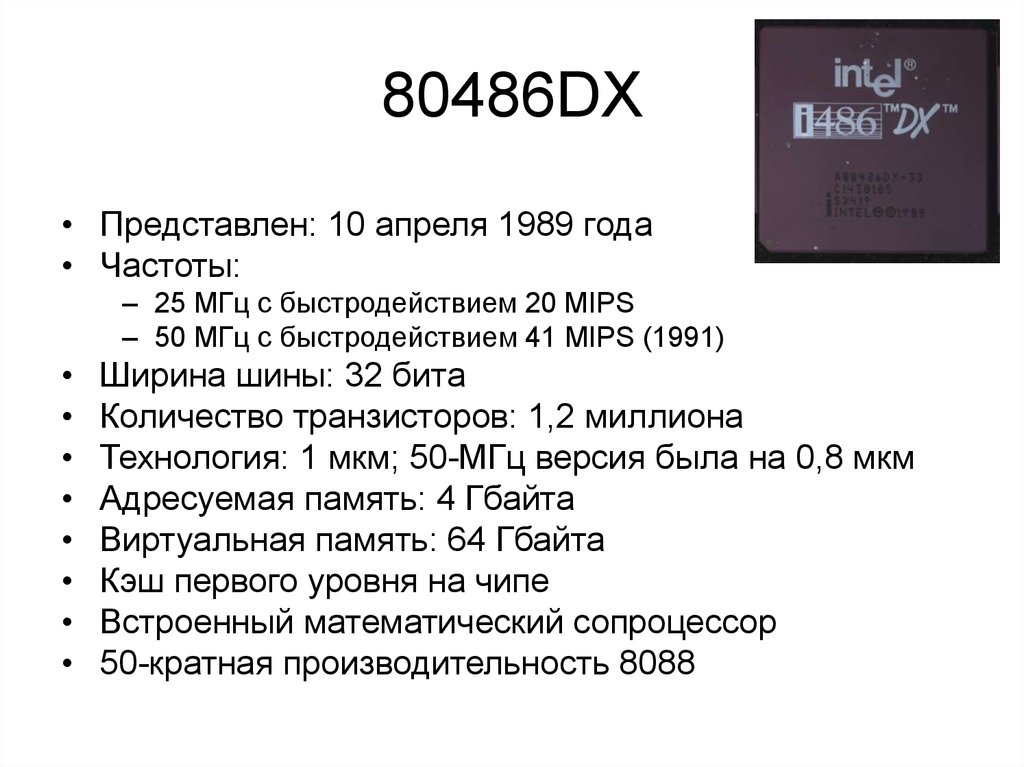 001 mm
  6 μm
6 μm i486SX[edit]
| i486SX Processors | |||||||||||||||
|---|---|---|---|---|---|---|---|---|---|---|---|---|---|---|---|
| Model | Launched | Process | Freq | Max Mem | |||||||||||
| i486SX-16 | 22 April 1991 | 1,000 nm
1 μm 800 nm 0.8 μm |
16 MHz
0.016 GHz |
4,096 MiB
4,194,304 KiB |
|||||||||||
| i486SX-20 | 16 September 1991 | 1,000 nm
1 μm 800 nm 0.8 μm |
20 MHz
0.02 GHz |
4,096 MiB
4,194,304 KiB |
|||||||||||
| i486SX-25 | 16 September 1991 | 1,000 nm
1 μm 800 nm 0.8 μm |
25 MHz
0.025 GHz |
4,096 MiB
4,194,304 KiB |
|||||||||||
| i486SX-33 | 21 September 1992 | 1,000 nm
1 μm 800 nm 0.8 μm |
33 MHz
0.033 GHz |
4,096 MiB
4,194,304 KiB |
|||||||||||
| i486SX2-50 | 800 nm
0.8 μm |
50 MHz
0.05 GHz |
4,096 MiB
4,194,304 KiB |
||||||||||||
| i486SX2-66 | 800 nm
0.8 μm |
66 MHz
0.066 GHz |
4,096 MiB
4,194,304 KiB |
||||||||||||
| Count: 6 | |||||||||||||||
 001 mm
 i486SL[edit]
| i486SL Processors | |||||||||||||||
|---|---|---|---|---|---|---|---|---|---|---|---|---|---|---|---|
| Model | Launched | Process | Freq | Max Mem | |||||||||||
| i486SL-20 | 9 November 1992 | 800 nm
0. |
20 MHz
0.02 GHz |
4,096 MiB
4,194,304 KiB |
|||||||||||
| i486SL-25 | 9 November 1992 | 800 nm
0.8 μm |
25 MHz
0.025 GHz |
4,096 MiB
4,194,304 KiB |
|||||||||||
| i486SL-33 | 9 November 1992 | 800 nm
0.8 μm |
33 MHz
0.033 GHz |
4,096 MiB
4,194,304 KiB |
|||||||||||
| Count: 3 | |||||||||||||||
 8 μm
8 μm i486GX[edit]
| i486GX Processors | |||||||||||||||
|---|---|---|---|---|---|---|---|---|---|---|---|---|---|---|---|
| Model | Launched | Process | Freq | Max Mem | |||||||||||
| i486GX-33 | 800 nm
0.8 μm |
33 MHz
0.033 GHz |
4,096 MiB
4,194,304 KiB |
||||||||||||
| Count: 1 | |||||||||||||||
 00391 TiB
 - Am486
This list is incomplete; you can help by expanding it.
Documents[edit]
Datasheet[edit]
- 486 DX2 Microprocessor Data Book (February 1992)
- Intel486 DX2 Microprocessor Data Book (July 1992)
- 486 DX Microprocessor Data Book (October 1992)
- i486 MICROPROCESSOR (April 1989)
Manual[edit]
- Intel486 Microprocessor Family Programmer’s Reference Manual (1992)
- i486 MICROPROCESSOR PROGRAMMER’S REFERENCE MANUAL (1990)
- i486 MICROPROCESSOR HARDWARE REFERENCE MANUAL (1990)
80486 — Intel — WikiChip
| Intel 80486 | |
| Intel A80486DX-25 | |
| Developer | Intel |
| Manufacturer | Intel |
| Type | Microprocessors |
| Introduction | April 10, 1989 (announced) June, 1989 (launch) |
| Production | 1988-2007 |
| Architecture | x86 |
| ISA | IA-32 |
| µarch | 80486 |
| Word size | 32 bit
4 octets |
| Process | 1 µm
1,000 nm , 800 nm 0.8 μm , 600 nm 0.6 μm |
| Technology | CMOS |
| Clock | 16 MHz-100 MHz |
| Package | PGA-168, PQFP-196, SQFP-208 |
| Succession | |
| ← | → |
| 80386 | Pentium |
 001 mm
 The 80486, also i486 and 486, (pronounced eighty-four-eighty-six) was a family of 32-bit 4th-generation x86 microprocessors introduced by Intel in 1989 as a successor to the 80386. 486 introduced a number of enhancements to 386 including a new level 1 cache, better IPC performance, and an integrated FPU. The 486 became the first x86 chip family to exceed one million transistors.
Contents
- 1 Architecture
- 2 Members
- 2.1 i486DX
- 2.2 i486SX
- 2.3 i486SL
- 2.
 4 i486GX
- 3 Clones
- 4 Documents
- 4.1 Datasheet
- 4.2 Manual
Architecture[edit]
- Main article: 80486 Microarchitectures
Like its predecessor, the 80486 maintains full backwards object code comparability with the all previous x86 processors (80386, 80286, 80186, etc…). To improve performance Intel introduced a new layer of cache on-die (previously various external extensions existed). The 8 KB, 4-way set associative, write-back policy, cache was unified for both the data and instructions. This provided much needed faster access to recently used data and instructions. Various enhancements were also made to the bus interface including faster communication that required single clock cycle instead of multiple.
Whereas before a separately packaged math coprocessor was used (i.e. 80387, 80287, etc..), the 80486 moved the unit on-die eliminating the external communication delays altogether. Furthermore more aggressive math algorithms were used to implement the new FPU yielding faster floating point calculations.
The pipeline itself received some attention as well. Simple ALU register, register and register, immediate cached operations could now complete in a single cycle; this previously required at least 2 cycles.
Members[edit]
i486DX[edit]
| i486DX Processors | |||||||||||||||
|---|---|---|---|---|---|---|---|---|---|---|---|---|---|---|---|
| Model | Launched | Process | Freq | Max Mem | |||||||||||
| i486DX-20 | June 1989 | 1,000 nm
1 μm 800 nm 0.8 μm |
20 MHz
0.02 GHz |
4,096 MiB
4,194,304 KiB |
|||||||||||
| i486DX-25 | June 1989 | 1,000 nm
1 μm 800 nm 0.8 μm |
25 MHz
0.025 GHz |
4,096 MiB
4,194,304 KiB |
|||||||||||
| i486DX-33 | 7 May 1990 | 1,000 nm
1 μm 800 nm 0.8 μm |
33 MHz
0.033 GHz |
4,096 MiB
4,194,304 KiB |
|||||||||||
| i486DX-50 | 24 June 1991 | 1,000 nm
1 μm 800 nm 0.8 μm |
50 MHz
0.05 GHz |
4,096 MiB
4,194,304 KiB |
|||||||||||
| i486DX2-40 | 3 March 1992 | 1,000 nm
1 μm 800 nm 0.8 μm |
40 MHz
0.04 GHz |
4,096 MiB
4,194,304 KiB |
|||||||||||
| i486DX2-50 | 3 March 1992 | 1,000 nm
1 μm 800 nm 0.8 μm |
50 MHz
0.05 GHz |
4,096 MiB
4,194,304 KiB |
|||||||||||
| i486DX2-66 | 3 March 1992 | 1,000 nm
1 μm 800 nm 0.8 μm |
66 MHz
0.066 GHz |
4,096 MiB
4,194,304 KiB |
|||||||||||
| i486DX4-100 | 7 March 1994 | 600 nm
0.6 μm |
100 MHz
0.1 GHz |
4,096 MiB
4,194,304 KiB |
|||||||||||
| i486DX4-75 | 7 March 1994 | 600 nm
0.6 μm |
75 MHz
0.075 GHz |
4,096 MiB
4,194,304 KiB |
|||||||||||
| Count: 9 | |||||||||||||||
 001 mm
  00391 TiB
 i486SX[edit]
| i486SX Processors | |||||||||||||||
|---|---|---|---|---|---|---|---|---|---|---|---|---|---|---|---|
| Model | Launched | Process | Freq | Max Mem | |||||||||||
| i486SX-16 | 22 April 1991 | 1,000 nm
1 μm 800 nm 0.8 μm |
16 MHz
0.016 GHz |
4,096 MiB
4,194,304 KiB |
|||||||||||
| i486SX-20 | 16 September 1991 | 1,000 nm
1 μm 800 nm 0.8 μm |
20 MHz
0.02 GHz |
4,096 MiB
4,194,304 KiB |
|||||||||||
| i486SX-25 | 16 September 1991 | 1,000 nm
1 μm 800 nm 0.8 μm |
25 MHz
0.025 GHz |
4,096 MiB
4,194,304 KiB |
|||||||||||
| i486SX-33 | 21 September 1992 | 1,000 nm
1 μm 800 nm 0.8 μm |
33 MHz
0.033 GHz |
4,096 MiB
4,194,304 KiB |
|||||||||||
| i486SX2-50 | 800 nm
0.8 μm |
50 MHz
0.05 GHz |
4,096 MiB
4,194,304 KiB |
||||||||||||
| i486SX2-66 | 800 nm
0.8 μm |
66 MHz
0.066 GHz |
4,096 MiB
4,194,304 KiB |
||||||||||||
| Count: 6 | |||||||||||||||
 001 mm
 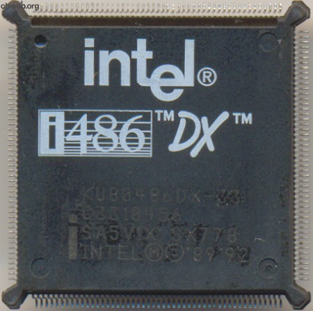 00391 TiB
 i486SL[edit]
| i486SL Processors | |||||||||||||||
|---|---|---|---|---|---|---|---|---|---|---|---|---|---|---|---|
| Model | Launched | Process | Freq | Max Mem | |||||||||||
| i486SL-20 | 9 November 1992 | 800 nm
0.8 μm |
20 MHz
0.02 GHz |
4,096 MiB
4,194,304 KiB |
|||||||||||
| i486SL-25 | 9 November 1992 | 800 nm
0. |
25 MHz
0.025 GHz |
4,096 MiB
4,194,304 KiB |
|||||||||||
| i486SL-33 | 9 November 1992 | 800 nm
0.8 μm |
33 MHz
0.033 GHz |
4,096 MiB
4,194,304 KiB |
|||||||||||
| Count: 3 | |||||||||||||||
 8 μm
8 μm i486GX[edit]
| i486GX Processors | |||||||||||||||
|---|---|---|---|---|---|---|---|---|---|---|---|---|---|---|---|
| Model | Launched | Process | Freq | Max Mem | |||||||||||
| i486GX-33 | 800 nm
0.8 μm |
33 MHz
0.033 GHz |
4,096 MiB
4,194,304 KiB |
||||||||||||
| Count: 1 | |||||||||||||||
- Am486
This list is incomplete; you can help by expanding it.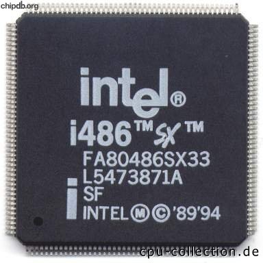
Documents[edit]
Datasheet[edit]
- 486 DX2 Microprocessor Data Book (February 1992)
- Intel486 DX2 Microprocessor Data Book (July 1992)
- 486 DX Microprocessor Data Book (October 1992)
- i486 MICROPROCESSOR (April 1989)
Manual[edit]
- Intel486 Microprocessor Family Programmer’s Reference Manual (1992)
- i486 MICROPROCESSOR PROGRAMMER’S REFERENCE MANUAL (1990)
- i486 MICROPROCESSOR HARDWARE REFERENCE MANUAL (1990)
80486 | Wiki | Fandom
Template:CPU Card
Intel 80486 (also known as i486, Intel 486 or simply 486th) is a fourth generation 32-bit scalar x86-compatible microprocessor built on a hybrid CISC-RISC core and released by Intel on April 10, 1989. This microprocessor is an improved version of the 80386 microprocessor. It was first demonstrated at the Comdex Fall exhibition in the fall of 1989. It was the first microprocessor with a built-in math coprocessor (FPU).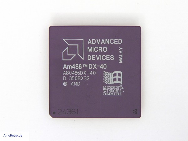 Used primarily in desktop PCs, high performance workstations, servers and portable PCs (notebooks and laptops).
The project manager for the Intel 486 microprocessor was Template:Not translated 2.
Contents
- 1 Description
- 1.1 Specifications (summary)
- 1.2 Differences between Intel 486DX and Intel 386 [2]
- 2 Microarchitecture
- 3 Mathematical model and instruction set
- 4 Blocks and implementation of interfaces
- 4.1 Registers
- 4.2 Instruction Pipelining
- 4.3 Processor cache
- 4.4 Math coprocessor
- 4.5 Building a computer system
- 5 Models
- 6 Competitive solutions
- 7 Notes
- 8 Literature
- 9 Links
Description[]
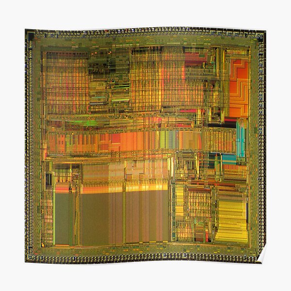
File:80486dx2-large.jpg
Intel 80486DX2 microprocessor die
File:80486 open.jpg
Chip location in the microprocessor package
Specifications (summary)[]
[1]
- First model announced: April 10, 1989
- Register width: 32 bits
- Width of external data and address buses: 32 bits
- Virtual addressable memory: 64 TB
- Maximum segment size: 4 GB
- Physical addressable memory: 4 GB
- L1 cache: 8 KB, DX4 — 16 KB
- L2 cache: on motherboard (at FSB frequency)
- FPU: on-chip, SX disabled
- Processor clock frequency, MHz: 16—33
- Clock frequency FSB, MHz: 16-50
- Supply voltage: 5-3.
 3 V
3 V - Number of transistors: 1.185M, SX2 — 0.9M, SL — 1.4M, DX4 — 1.6M
- Process technology, nm: 1000, 800 and 600 for DX4
- Chip area: 81 mm² for 1.185 MTS and 1000 nm technology, 67 mm² for 1.185 MTS and 800 nm technology, 76 mm² for DX4
- Maximum current consumption: no data
- Maximum power consumption: no data
- Connector: Socket
- Package: 168- and 169-pin ceramic PGA, 132- and 208-pin plastic PQFP
- Instructions: x86 (150 instructions, not including modifications)
The processor had 32-bit address and data buses. This required memory in the form of four 30-pin or one 72-pin SIMMs.
Differences between Intel 486DX and Intel 386
[2] []
The Intel 486DX, 486DX2, and Intel DX4 are a die that contains the CPU, math coprocessor, and cache controller. Fully compatible at the preprocessor level with Intel 386 processors, however, they have the following differences:
- Intel 486 processors, unlike the Intel ULP486GX, which only supports a 16-bit data bus, dynamically change the size of the used bus to support 8-, 16-, and 32-bit transactions.
 Intel 386s only support two bus widths, 16 and 32 bits, and do not require any external logic to manage bus width changes.
 - Intel 486 processors have a short transfer mode that allows four 32-bit words from external memory to cache to be transferred over the bus in one transaction using only five cycles. The Intel 386 requires a minimum of eight cycles to transfer the same amount of data.
- The Intel 486 processor has a BREQ signal used to support multiprocessor systems.
- The Intel 486 processor bus is significantly more powerful than the Intel 386 processor bus. New features in the form of bus frequency multiplication, parity check (not present in ULP486SX and ULP486GX), shorter data transfer cycle, cached cycles, including cached cycle without data check, support for transactions over 8-bit bus.
- To support the on-chip cache, new control registers (CD and NW) have been introduced, new pins for the bus, new types of bus exchange cycles have been added.
- The instruction set of the Intel 387 math processor is not only fully supported, but also extended. No I/O cycles are performed during the execution of a floating point instruction. Interrupt 9 not enabled, interrupt 13 occurs.
- The Intel 486 processor supports new error detection modes to ensure DOS compatibility. These new modes require a new bit in control register 0 (NE).
- Six new commands added to the command set: BSWAP (Byte Swap), XADD (Exchange and Add), CMPXCHG (Compare and Exchange), INVD (Invalidate data cache), WBINVD (Write-back and Invalidate data cache) and INVLPG (Invalidate TLB Entry).
- In control register 3, two new bits are assigned that are responsible for caching the current page directory.
- Added new page protection features that require a new bit in control register 0.
- Added new alignment checking capabilities that require a new bit in the flag register and control register 0.
- Replaced the algorithm for TLB with a pseudo-LRU (PLRU) algorithm similar to that used in the on-chip cache.
- Three new test registers have been added to test the on-chip cache: TR5, TR6, and TR7. Improved TLB stability.
- The prefetch queue has been increased from 16 bytes to 32 bytes. To ensure correct execution of new instructions, jumps are always performed after code modification.
- After a reset, the value <04> is written to the top of the ID byte.
The length of the instruction queue has been increased to 32 bytes.
Blocks and implementation of interfaces[]
Intel486 BB device interface.png
Interface with I/O devices
Intel486 32-bit IO Interface.png
Interface with 32-bit I/O devices
Intel4
Bus Swapping 16-bit interface.png
Variable data bus interface: 16 bit
Intel486 8-bit device interface.png
Organization of an interface with 8-bit I/O devices
Registers []
The processor has an extended instruction set compared to 80386, which has several additional registers, namely, three 32-bit test registers (TR5 , TR4, TR3).
 New flags have also been added in the flag register (EFLAGS) and other control registers (CR0, CR3).
Due to the inclusion of the coprocessor in the processor chip, the Intel 486 can also access the FPU registers: data registers, tag register, status register, FPU command and data pointers, FPU control register.
Instruction Pipelining[]
The Intel 486 has improved the instruction execution mechanism in several steps. The Intel 486 series processor pipeline consisted of 5 stages: instruction fetch, instruction decoding, instruction operand address decoding, instruction execution, instruction execution result recording. The use of a pipeline made it possible to perform preparatory operations on another instruction during the execution of one instruction. This greatly increased the performance of the processor.
Intel486 Fully Associative Cache.png
Fully Associative Cache
The Intel 486 had an on-chip cache of 8 KB, later 16 KB, running at the core frequency.
 The presence of the cache made it possible to significantly increase the speed of operations by the microprocessor. Initially, the Intel 486 cache was write-through (Pattern:Lang-en), but later, within the Intel 486 family, models with an internal write-back cache (Pattern:Lang-en) were released. The processor could also use an external cache, the read-write speed of which, however, was noticeably lower than that of the internal cache. At the same time, the internal cache began to be called the first level cache (Level 1 Cache), and the external cache located on the motherboard, the second level cache (Level 2 Cache). The cache had a 4-channel set-associative architecture and worked at the level of physical memory addresses.
However, as a result of using the integrated cache memory, the number of transistors in the processor has increased significantly and, as a result, the crystal area has increased. The increase in the number of transistors has led to a significant increase in power dissipation.
 On average, power dissipation has increased by 2 times compared to similar models of the 80386 series. In many ways, this was facilitated by the integration of cache memory, although there were other factors, but they are not so significant. For this reason, older Intel 486 processors already required forced (active) cooling.
Math Coprocessor[]
The built-in math coprocessor was used on the Intel 486 (Pattern:Lang-en). In general, it was the first microprocessor of the x86 family with an integrated FPU. The built-in FPU was software compatible with the Intel 80387 chip, the math coprocessor used in systems with the 80386 processor. Using the built-in coprocessor made the system cheaper and faster by reducing the overall number of pins and chip packages.
Initially, all manufactured Intel 486 microprocessors were equipped with a working coprocessor, these processors were named Intel 486DX. Later, in 1991, Intel decided to release processors with a disabled coprocessor, and these processors were named Intel 486SX.
 Systems built on these processors could be equipped with a separate coprocessor, for example, Intel 487SX or a coprocessor from other manufacturers.
Building a computer system[]
File:SIS chipset based MB for 486 CPUs.JPG
Motherboard based on SIS chipset (85C496 and 85C497) for i486 class processors
Intel 486-based systems were originally equipped with only 8- and/or 16-bit ISA buses. Later motherboards combined the slow ISA bus with the high-speed VESA (or VLB — Template:Lang-en) bus, primarily for video cards and hard drive controllers. The latest motherboards for i486 processors were equipped with PCI and ISA buses, and sometimes VESA. The speed of the ISA bus was determined by multipliers, and the operating frequency of the PCI and VLB buses was equal to the frequency of the i486 processor bus (although some motherboards had multipliers for them as well).
Later, i486 motherboards added support for the Plug-and-Play technology used in Windows 95, which allows computers to automatically detect and configure devices installed on the computer and install the appropriate drivers.
Intel486 System Controller.png
Building an Intel 486 System Controller
Intel486 System Arbitration.png
Organization of an arbitration system
Block diagram of EBC — EISA Bus Controller.png
Organization of the tire controller EISA
ISA Bridge Schematic.png
Organization of the Interface (bridge) PCI-ESA
Intel486 WITH 82C59A.png
Building 82C59A
Intel486 ANTEL486 ANTEL486 ANTEL486 ANTEL486 systems using interrupt controller cascading
Intel486-Typ EISA System.png
Building a typical configuration using the EISA bus
Intel486-Typ PCI System.png
Building a typical configuration using the PCI bus
Intel486 Address decider schematic.png
Building an address decoder
Intel486 Logic A1 BHE BLE for 16-bit.png
Building a signal decoder BHE# and BLE#
Intel486 Logic for 74S138.png
Construction of control circuits and truth table on the example of using IC 74S138
Models[]
Summary table of Intel 486 processor models [3] [4] [5] [6] Model Codename Intel S-Spec Housing type Processor socket type Frequency, MHz Data bus (external), bit Supply voltage, volts Process lithography standards, micron Number of transistors Announcement date Note, difference Intel 486DX Intel A80486DX-25 P4 SX328 Ceramic housing PGA-168 Socket 1,
Socket 2,
Socket 325 × 1 32 5 1 1,185,000 Template:Date The original processor of the i486 family.  First level cache 8 KB.
Intel A80486DX-33 P4 SX329 Ceramic housing PGA-168 Socket 1,
Socket 2,
Socket 333 × 1 32 5 1 1,185,000 Template:Date Intel A80486DX-33 P4 SX729 Ceramic bodyc PGA-168 Socket 1,
Socket 2,
Socket 333 × 1 32 5 1 1,185,000 Template:Date DX logo on body. Intel A80486DX-33 (SL enhanced) P4 SX810 Ceramic housing PGA-168 Socket 1,
Socket 2,
Socket 333 × 1 32 5 1 1,185,000 Template:Date «&E» marking and DX logo on the case. Intel A80486DX-50 P4 SX710 Ceramic housing PGA-168 Socket 2,
Socket 350 × 1 32 5 0.  8
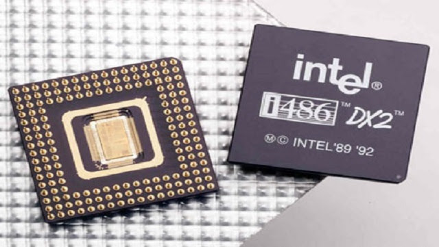
8 1,185,000 Template:Date DX logo on body. Intel 486DX2 Intel SB80486DX2-40 P24 SX809 Plastic housing PQFP-208 On adapter board 20 × 2 32 3.3 0.8 1,200,000 Template:Date On adapter board. Intel SB80486DX2-50 P24 SX920 Plastic housing PQFP-208 On adapter board 25 × 2 32 3.3 0.8 1,200,000 Template:Date On adapter board. Intel A80486DX2-50 P24 SX808 Ceramic housing PGA-168 Socket 1,
Socket 2,
Socket 325 × 2 32 5 0.8 1,200,000 Template:Date The
had no DX-50 problems with ISA 16 bit and VESA VL-Bus due to operation at 25 MHz, but was 3.  ..15% slower in real applications. The bulk was released by the OEM system manufacturer. Also produced by IBM with the appropriate marking on the case, type:
«COPYRIGHT INTEL ’89 ’92
1 MFG BY IBM»Intel A80486DX2-66 P24 SX807 Ceramic housing PGA-168 Socket 1,
Socket 2,
Socket 333 × 2 32 5 0.8 1,185,000 Template:Date Intel A80486DX2-66 P24 SX955 Ceramic housing PGA-168 Socket 1,
Socket 2,
Socket 333 × 2 32 5 0.8 1,200,000 Template:Date Write-back processor cache. Additional markings on the case «&EW»: SL enhanced CPU technology is used. Intel A80486DX2-66 P24 SX759 Ceramic housing PGA-168 Socket 1,
Socket 2,
Socket 333 × 2 32 5 0. 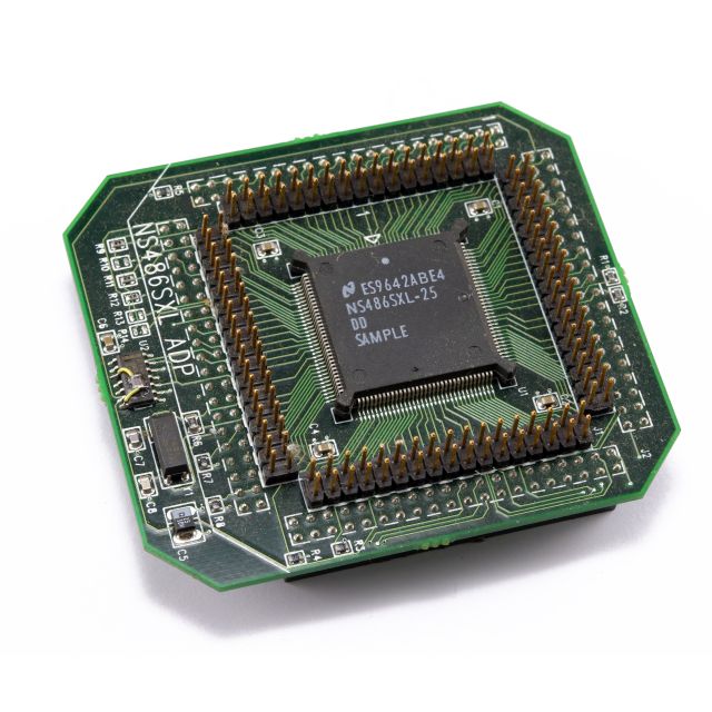 8
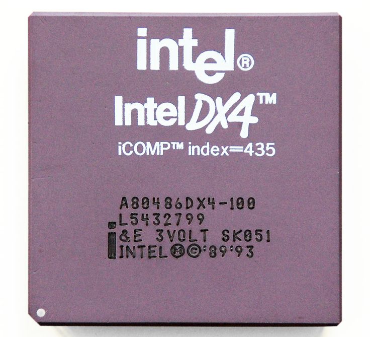
8 1,200,000 Template:Date A blue (factory-made in the USA) or black (Malaysia) heatsink is integrated on the ceramic body. Intel DX4 Intel A80486DX4-75 P24C SX884 Ceramic housing PGA-168 Socket 1,
Socket 2,
Socket 325 × 3 32 3 0.6 1,600,000 Template:Date Additional case markings «&EW»: Uses SL enhanced CPU technology. Intel FC80486DX4-75 Mobile P24C SK052 Plastic housing PQFP-208 On adapter board 25 × 3 32 3 0.6 1,600,000 Template:Date Mobile system adapter Intel FC80486DX4-75 Mobile Module P24C SX883 Plastic housingc PQFP-208 On adapter board 25 × 3 32 3 0. 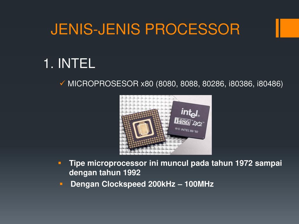 6
6 1,600,000 Template:Date Used in IBM Thinkpad 755 Intel A80486DX4-100 P24C SX900 Plastic housing PQFP-208 On adapter board 33 × 3 32 3 0.6 1,600,000 Template:Date Mobile system adapter Intel FC80486DX4-100 Mobile Module P24C SX883 Ceramic housing PGA-168 Socket 1,
Socket 2,
Socket 333 × 3 32 3 0.6 1,600,000 Template:Date Additional case markings «&EW»: Uses SL enhanced CPU technology. Intel RapidCAD-1 N/A SZ624 PGA-132 ceramic body i386/387 33 × 3 32 N/A N/A 1,600,000 1991 The
Intel RapidCad is a specially packaged Intel 486DX, without cache and with a stub instead of an FPU, a standard i386 pinout, designed to replace the Intel 80386 and 80387 FPU processors. 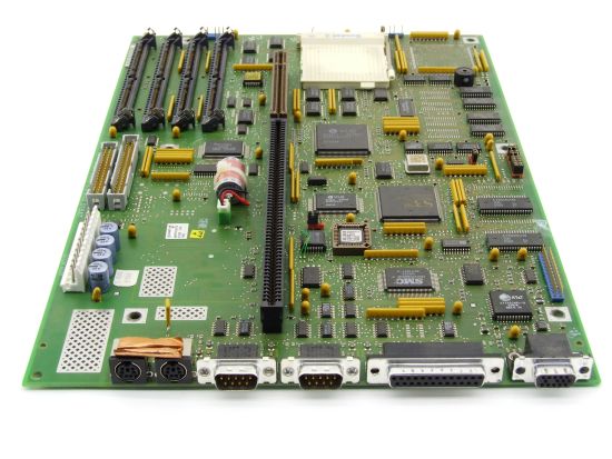
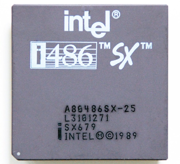
Intel RapidCAD-2 N/A SZ625 Ceramic housing PGA-68 i376/387 33 × 3 32 N/A N/A 1,600,000 Template:Date Intel486SX Intel A80486SX-20 P23 SX406 Ceramic housing PGA-168 Socket 1,
Socket 2,
Socket 320 × 1 32 5 1 1,185,000 Template:Date Like i486DX, but with math coprocessor disabled. Intel A80486SX-25 P23 SX679 Ceramic housing PGA-168 Socket 1,
Socket 2,
Socket 325 × 1 32 5 1 1,185,000 Template:Date Intel A80486SX-25 P23 SX903 Ceramic housing PGA-168 Socket 1,
Socket 2,
Socket 325 × 1 32 5 1 1,185,000 Template:Date Intel KU80486SX-25 P23 SX406 PQFP-196 plastic case inside PGA-168 Socket 1,
Socket 2,
Socket 325 × 1 32 5 1 1,185,000 Template:Date Overclocking to 40 MHz Intel A80486SX-33 P23 SX797 Ceramic housing PGA-168 Socket 1,
Socket 2,
Socket 333 × 1 32 5 1 1,185,000 Template:Date Intel SB80486SX-33 P23 SX855 Plastic housingc PQFP-208 On adapter board 33 × 1 32 5 1 1,185,000 Template:Date Intel A80486SX2-50 P23 SX845 Ceramic housing PGA-168 Socket 1,
Socket 2,
Socket 325 × 2 32 5 1 900,000 Template:Date Intel 486SX2-50/SA OEM P23 SX845 Ceramic housing PGA-168 Socket 1,
Socket 2,
Socket 325 × 2 32 5 1 900,000 Template:Date Integrated heatsink. 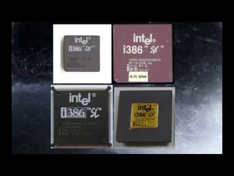 Supplied mainly to OEMs.
Other, manufactured by Intel Intel 487SX P23N Template:Date i486DX with changed pinout for use as FPU in i486SX systems. Intel 486 OverDrive P23T Template:Date Designed to upgrade computers with i486DX/SX processors. Intel KU80486SL-25 N/A SX709 Ceramic housing PGA-168 Socket 1,
Socket 2,
Socket 325 × 1 32 5 0.8 1,400,000 Template:Date i486SX low power consumption, mainly used in laptop computers. Intel 486DX SL-enhanced P4S Template:Date i486DX with SL technology. 
Intel 486SX SL-enhanced P23S Template:Date i486SX with SL technology. Intel 486DX2 SL-enhanced P24S Template:Date i486DX2 with SL technology. Frequency 50-66 MHz; supply voltage 5 volts. Intel 486SX2 ??? 1994 Like i486DX2, but with math coprocessor disabled. Intel DX4 P24C Template:Date Triple external bus clock, 75-100 MHz; supply voltage 3.3 volts. Intel 486DX2 wb P24D Template:Date i486DX2 with write-back cache. Frequency 50-66 MHz; supply voltage 5 volts. 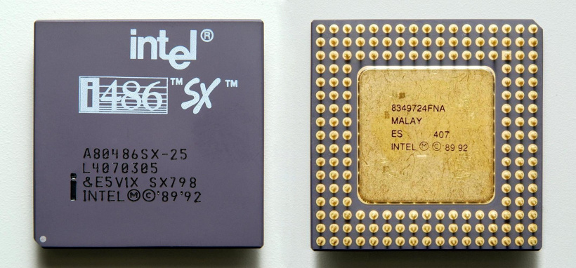
Intel DX4 OverDrive PR P4T Template:Date Designed to upgrade computers with i486DX/SX processors. Intel 486GX ??? Template:Date i486SX for use in portable devices. Pentium OverDrive 62.5/82.5 for 5V 486 /3.3V DX4 P24T Designed to upgrade computers with Intel DX4 processors to a Pentium processor with a frequency of 62.5 or 82.5 MHz. Since the introduction of the first Intel 486DX processor, many other models of the 486 family have been released with the suffixes SX, SL, DX2, DX4, GX. They differed in their functional purpose and some technological parameters (supply voltage, clock frequency, cache memory size, absence or presence of a coprocessor, etc.
 ).
).
486DX2 processors had a multiplier of 2 — that is, for example, at a system bus frequency of 33 MHz, the operating frequency of the processor itself was 66 MHz. Later, Intel DX4 processors appeared — however, their multiplier was not 4, but 3. As a result of the introduction of multipliers, for the first time such a concept as overclocking (Template:Lang-en) came into common use — increasing processor performance by increasing the bus clock frequency or coefficient multiplication. So, it is known that in Russia, even systems in which i486 processors operated at frequencies up to 160 MHz went on open sale.
Competitors[]
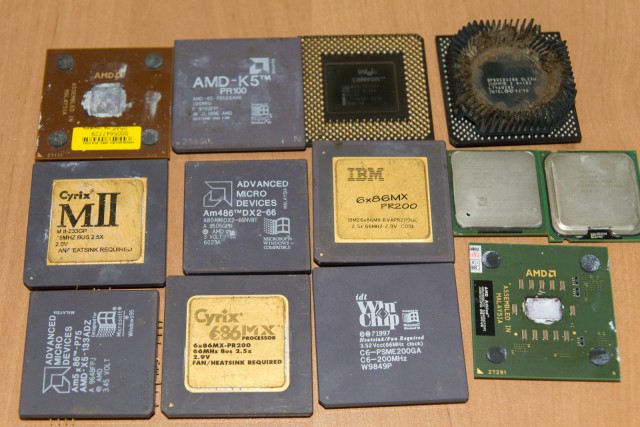
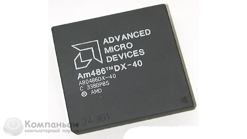
By the time the 486 was released, Intel had lost ownership of the x86 trademarks and many vendors used similar names. The main slogan of Intel’s competitors was «Practically the same as Intel, only for less money.»
486-compatible processors were also made by companies such as IBM, Texas Instruments, AMD, Cyrix, UMC, and Chips and Technologies.
 Some of them were almost exact copies both in terms of performance and specifications, while others, on the contrary, differed from the original.
Already after Intel’s 486 processors left the mass market, AMD released the 486DX4-120 and Am5x86-133 processors.
In May 2006, Intel announced that production of the 80486 chips would cease at the end of September 2007. While this chip had long been obsolete for personal computer applications, Intel continued to manufacture it for use in embedded systems.
486 Prozessoren von AMD Cyrix IBM Intel ST Texas Instruments.jpg
486 AMD Cyrix processors IBM Intel ST Texas Instruments
I486-cpu-col1.jpg
i486 processors surrounded by processors from other manufacturers. [7]
UMC Green CPU 486 40 MHz.jpg
UMC Green CPU
Notes[]
- ↑ Microprocessor Types and Specifications
- ↑ Intel «EMBEDDED Intel486 PROCESSOR FAMILY. DEVELOPER’S MANUAL» Order No: 273021-001
- ↑ Intel IT Galaxy -> Marking the 40th anniversary of the first Intel microprocessor.
 Part 1
- ↑ cpu-collection.de >> 486
- ↑ Processor Collection (8086-80486)
- ↑ DX, DX2, DX4 processors
- ↑ Above — AMD Am486DX2-50 in a proprietary case with cache included. Below are typical representatives of the 4th generation. In the center — server solutions from Intel. On the right is the spatula that came with the Intel 486 OverDrive to remove the processor from the slot.
Literature[]
- Documentation issued by Intel:
- Order No: 271329-002 «MILITARY Intel486 PROCESSOR FAMILY»
- Order No: 272755-001 «Embedded Ultra-Low Power Intel486 GX Processor»
- Order No: 272731-002 «Embedded Ultra-Low Power Intel486 SX Processor»
- Order No: 272731-001 «Embedded Ultra-Low Power Intel486 SX Processor»
- Order No: 271329-003 «MILITARY Intel486 PROCESSOR FAMILY»
- Order No: 241199-002 «Intel486 Family of Microprocessors. Low power version. Data Sheet»
- Order No: 273025-001 «EMBEDDED Intel486 PROCESSOR.
 HARDWARE REFERENCE MANUAL»
 - Order No: 273021-001 «EMBEDDED Intel486 PROCESSOR FAMILY. DEVELOPER’S MANUAL»
- Order No: 272815-001 «Ultra-Low Power Intel486 SX PROCESSOR. EVALUATION BOARD MANUAL»
- Order No: 272771-002 «Embedded Write-Back Enhanced IntelDX4 Processor»
- Order No: 272771-001 «Embedded Write-Back Enhanced IntelDX4 Processor»
- Order No: 272770-002 «Embedded IntelDX2 Processor»
- Order No: 272770-001 «Embedded IntelDX2 Processor»
- Order No: 272769-002 «Embedded Intel486 SX Processor»
- Order No: 272769-001 «Embedded Intel486 SX Processor»
- Order No: 272755-002 «Embedded Ultra-Low Power Intel486 GX Processor»
- Order No: 240440-006 «Intel486DX MICROPROCESSOR»
Links[]
- Litigation history between Intel and AMD
- Processor Documentation at bitsavers.org Template:Ref-en
Intel 80486 Processor Architecture — Schematic, Registers
ComputerPress №3 1993.
 A. Borzenko
 The i80486 microprocessor integrated circuit was announced by Intel in
1989 at Comdex in Chicago. And although, obviously, we have not long already
it remains to wait for the appearance of the new 586th microprocessor, today
Today one of the most powerful universal microprocessors is the i80486.i80486 microprocessor architecture
“Architecture intertwines functional, technical and aesthetic
the beginning is usefulness, strength, beauty.
(From the dictionary)The i80486 microprocessor is a worthy successor to the i80x86 family, since
it allows you to create computing systems much more
productive than, say, on the i80386 microprocessor. Basically
the i80486 chip consists of a complete i80386 microprocessor,
i80387 arithmetic coprocessor and i82385 cache controller.
It is clear that we are not talking about a mechanical connection of functional
devices on a single chip. High degree of integration (more than a million
transistors) is not just a technological achievement, but an opportunity
implement new architectural solutions that improve
microprocessor performance. For example, in a microprocessor
i80486 uses pipelined command processing, quite widely
used in RISC processors. At the same clock frequency with
i80386 The i80486 microprocessor is three to four times faster.
This is due to a decrease in the number of cycles (cycles) required for
executing a command (instruction).Three in one
On fig. 1 shows an exemplary block diagram of the i80486 microprocessor, on
which it is quite easy to single out its main functional units —
memory management unit (MMU), module
arithmetic coprocessor (Floating Point Unit, FPU) and cache block
(Cache Unit). Although the i80486 microprocessor has all the
properties inherent in i80386, of course, there are differences. For example, in
the instruction set of the i80486 microprocessor along with the known instructions for
i80386, several additional commands included. However, the device
memory management MMU is fully compatible with the same device in
i80386. The same can be said about the FPU. And this, generally speaking, means that
all software running on a series of microprocessors
80×86/80×87 will work on i80486 without making any changes.Rice. 1. Block diagram of the microprocessor 80486 enlarge figure
The memory management unit MMU consists in turn of the device
Segmentation Unit and Paging
unit). Thanks to the division of memory into segments (segmentation), program codes and
data areas can be located almost anywhere in the logical
address space. In other words, with segmented memory organization
each module occupies its own contiguous area of memory, while
pagination breaks the module into separate pages. AT
in turn, the page manager allows you to implement
a memory paging mechanism that functions on more
low level and is transparent to the segmentation process.
This makes it possible to manage the physical address space. Should
also note that paging can be
disabled by software.Each memory segment can be subdivided into one or more 4K blocks.
 And memory, in turn, can
be organized into one or more such segments, the size
which can be up to 4 GB. Moreover, each such segment can
be given appropriate attributes that determine its location
in memory, value, type (stack, code, data) and protection characteristic.
Each task running on the i80486 can in principle consist of 16
381 segments, 4 GB each. So the range of the virtual
addressing reaches 64 TB. microprocessor segmentation device
supports four application and system mode protection mechanisms each
from friend. Thanks to this, based on the i80486 microprocessor, it is possible
building highly secure systems.Fundamentally, the i80486 microprocessor has two modes of operation: real
mode (Real Mode, otherwise 8086-Mode) and protected (Protected Mode). Wherein
in real mode it just behaves like a very fast microprocessor
i8086. From this mode i80486 can easily switch to secure
a mode that has rich memory management capabilities. For example,
in this mode, it is possible to switch from one task to another, and their
processing will occur as processing of independent tasks on their i8086
microprocessors («virtual 8086-machines» mode). This name is associated
so that each task behaves in the same way as if it
was executed on its own i8086 processor (i8088, respectively).The arithmetic coprocessor device in the i80486 operates in parallel with
ALU and supports a large number of arithmetic instructions for various
operand types. These are, in particular, numerous transcendental functions,
such as sine, cosine, tangent, logarithm, etc. It should be noted that FPU
fully supports ANSI/IEEE 754-1985 standard
for floating point arithmetic.i80486 microprocessor internal cache size is 8
KB. It should be said right away that for some applications this size
cache memory is not sufficient at all. This applies primarily to CAD and
desktop publishing systems. However, in this case, when developing
corresponding system, you can use the i82485 cache controller and
external cache memory with a capacity of 64 or 128 KB. Internal cache
implemented as associative and works in write through mode (i.e.
Data is written to both cache and RAM at the same time.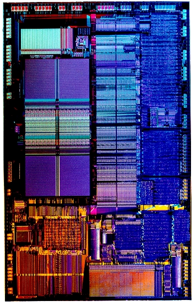 Cache in
The i80486 microprocessor certainly has some special features. AT
in particular, pages of memory can be designated as either «cached»,
or as «non-cached», and such a designation can be entered as
hardware as well as software. However, even the cache device itself can be
also disabled both hardware and software. According to some estimates,
using the built-in cache saves up to 80% of the time required
to access RAM.Registers, registers, registers…
The i80486 microprocessor contains, of course, all the registers available in
chips i80386 and i80387. Registers of the considered microprocessor
can be conditionally divided into three large groups: base registers,
system level registers and floating point registers. Consider these
register groups in more detail.The software model of the i80486 is determined mainly by the basic
registers shown in Fig. 2. That’s eight 32-bit
general purpose registers that can operate on data operands
sizes of 1, 2, and 4 bytes, or bit fields from 1 to 32. However, address operands
can only be either 2 or 4 bytes long. These
32-bit registers are designated as EAX, EBX, ECX, EDX, ESI,
EDI, EBP and ESP. Designations of the two low bytes of these registers to users
i8088/86/286 microprocessors are already well known. Of course, this is AX, BX,
CX, DX, SI, DI, BP and SP. Moreover, it should be noted that when accessing
the upper two bytes of these 32-bit registers, the contents of the two lower
bytes does not change. This ensures top-down compatibility with
i80286 microprocessor. Operations on byte operands (highest and
low bytes) are only available for four registers AX, BX, CX, DX,
moreover, the high bytes correspond to the designations AH, BH, CH and DH, and the low ones
— AL, BL, CL and DL.Rice. 2. Registers 80486
The Instruction Pointer (EIP) register is also 32-bit and points to the next instruction to be executed,
of course, indirectly. This register indicates only the offset relative to
the beginning of the address code segment, which is formed using
the contents of the CS register and the descriptor table element (more on
this a little later).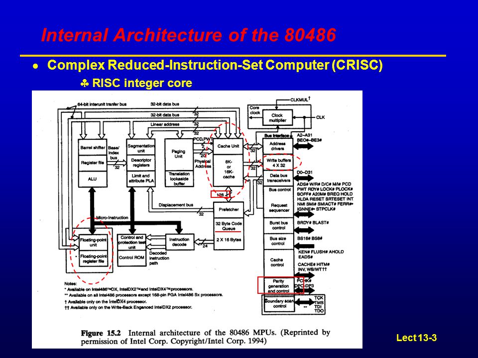 The low two bytes of the EIP register correspond to the 16-bit IP register, which is used only
with 16-bit addressing.To designate a basic 32-bit register
bit-by-bit indication of the state of the processor uses the so-called
flag register — EFLAGS. This register contains bits that characterize
the last operation performed by the processor, and some other service
information. On fig. 3 shows the bit designations in the EFLAGS register.
Let us explain the purpose of some of them. If the EFLAGS register is set
17th bit — VM (Virtual 8086 Mode), then
the i80486 microprocessor enters the «virtual 8086 machines» mode. Of course,
this is only possible in protected mode. Bit 16 — RF (Resume Flag)
usually used for debug modes. When it is set, the interrupt
caused by a fatal error is ignored and a jump to
following instruction. Bit 14 — NT (Nested Task) is used in i80486 for
monitoring multiple interrupted or called by CALL instruction
programs. Two bits 12 and 13 IOPL (Input/Output Privilege Level)
define access rights in protected mode to I/O instructions.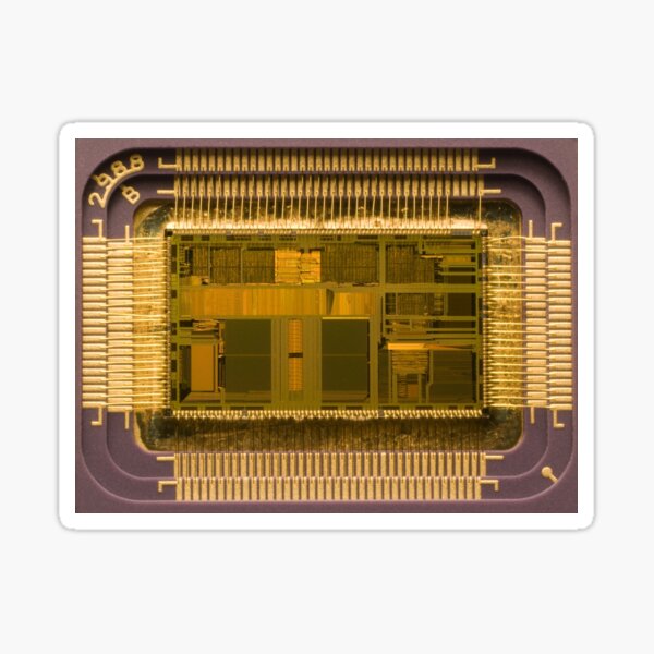
Rice. 3. Bits in the EFLAGS register
Of six 16-bit segment registers
four (DS, ES, FS and GS) are called data segment registers, CS —
code segment register, and SS is the stack segment register. How they work
these registers in i8086 microprocessor mode are fairly well known.
To get a 20-bit physical address
it is necessary to sum the 16-bit offset with
the base address stored in one of the segment registers. And
addition occurs so that the contents of the segment register are shifted
relative to the second term (shift) to the left by 4 bits. That is, by
essentially, the addition of the 20-bit base
address (the least significant 4 bits of which are, of course, always zeros) with a 16-bit offset, the result, of course, is
the required 20-bit address. While at work
microprocessor i80486 (and, of course, i80386) in protected mode
The executive physical address is formed somewhat differently. You can say
that it is made up of five components. First of all, we note that in
protected mode segment registers are called selector, or simply
selectors. The selector register points to the corresponding element in
one of the Descriptor Tables located in memory. Moreover, the basic
the address of this Table is stored either in the register of the Global Descriptor
Tables, or in the register of the Local Descriptor Table, although in general
case, it can be stored in another register of the microprocessor. Each element
Descriptor Table contains the base address of a particular segment, its
size and rights
access. The i80486 has a Global Descriptor Table entry of size 8
bytes and consists of a 32-bit base address,
A 20-bit segment size field and descriptor attributes. In field
segment size, for example, can be stored either the number of bytes (up to 1
MB) that contains this segment, or the number of pages by
4096 bytes each. Therefore, the segment size in protected mode
can vary from 1 byte to 4 GB. In this way,
the resulting protected mode address can be formed in the general
case by summing the contents of the base register with the contents of the index
register multiplied by the scale factor (1, 2, 4, or 8) plus
the offset in the command itself, plus the base address of the segment from the element
Descriptor Table (Fig. 4).
4).
Rice. 4. Address generation in secure mode
The i80486 microprocessor has three control registers (Control Registers)
system level — CR0, CR2, and CR3 (register CR1 is reserved by
Intel for further expansion). In the register CR0 of the available 32 bits
only 10 are used for control and status determination purposes (Fig.
5). Moreover, 5 of these 10 bits appeared only in i80486 (in i80386
They are not here). These beats are CD, NW, AM, WP and NE. Functionally, all these 10 bits
characterize the following: i80486 microprocessor modes — PG, PE, modes
built-in cache device — CD, NW, built-in device
float control — TS, EM, MP and NE control control
alignment — AM, supervisor write protection — WP. Low register word
CR0 is also used as a status word (status word)
microprocessor (Machine Status Word, MSW) in order to save
compatible with i80286 protected mode. Therefore, the LMSW and
SMSW (Load MSW, Store MSW) are only valid for the lower 16 bits of CR0 and
ignore new bits. In order to be able to work with these new
broken, the i80486 microprocessor instruction set includes a special
MOV instruction CR0, Reg.Rice. 5. CR0 register
The control register CR2 will accumulate the address at which the error occurred.
when paging memory. Control register CR3 is used
only when the PG bit is set in the CR0 register. In this case
register contains the base address of the page table that the
microprocessor for every task. The table itself is always aligned on
one page (4 KB).Four address system registers in i80386/486 microprocessors
are used for tables or segments that are stored in main memory.
This is the Global Descriptor Table (GDT),
Local Descriptor Table (LDT),
Interrupt Descriptor Table (IDT) and
Task State Segment (TSS). For symbols
the corresponding registers are abbreviated as GDTR, LDTR, IDTR and
TR. The GDTR and IDTR registers contain a 32-bit
base address, as well as a 16-bit boundary for
tables GDT and IDT. The GDT and IDT tables are available to all tasks
as global segments, while LDT and TSS are specific
tasks.