NVIDIA GeForce GTX 280 Graphics Cards by EVGA and PNY — Page 20 of 20
Power Consumption and Final Thoughts
Power Consumption
For testing power consumption, we took our test system and plugged it into a Seasonic Power Angel. For idle numbers, we allowed the system to idle on the desktop for 15 minutes and took the reading. For load numbers, we measured the peak wattage used by the system while running the game Call of Duty 4 at 1280×1024 with high graphics quality.
Power Consumption Results: Looking at total system power consumption levels, the PNY GeForce GTX 280 fits in great compared to the other cards, consuming a respectable amount of power. At idle the GeForce GTX 280 actually consumed the least amount of power! This is thanks in part to the fact that the GeForce GTX 200 GPUs include a more dynamic and flexible power management architecture than past generation NVIDIA GPUs. Four different performance / power modes are employed on the GTX 200 series:
-
Idle/2D power mode (approx 25 W)
-
Blu-ray DVD playback mode (approx 35 W)
-
Full 3D performance mode (variesworst case TDP 236 W)
-
HybridPower mode (effectively 0 W)
The new GTX 200 series of video cards have utilization monitors (digital watchdogs) that constantly check the amount of traffic occurring inside of the GPU. Based on the level of utilization reported by these monitors, the GPU driver can dynamically set the appropriate performance mode (i.e., a defined clock and voltage level) that minimizes the power draw of the graphics cardall fully transparent to the end user. The GPU also has clock-gating circuitry, which effectively shuts down blocks of the GPU which are not being used at a particular time (where time is measured in milliseconds), further reducing power during periods of non-peak GPU utilization. The ultimate in power savings would be to use use the card on a HybridPower motherboard to disable the card like we showed you in this recent article on HybridSLI and HybridPower.
Final Thoughts
After spending 20 pages talking about the GeForce GTX 280 it seems like we have just scratched the surface of what needs to be said for this card. If you haven’t noticed yet, graphics cards are getting complex. The move beyond just gaming makes it tough to just benchmark a few games and call it the next best thing. The brutal reality is that the industry is changing. Optimized PC design is the way things are moving and you either need to get on the bandwagon or get run over. For years the industry used to be about Enterprise Computing, which was all about productivity. Today, the industry is all about Visual Computing, which is gives creativity and self-expression with things like pictures, movies, gaming and so on. With Windows Vista and Mac OS X operating systems both enabling 3D content we all now have access to visual computing and we are soon to be surrounded by various applications and utilities that take it to the next level like PicLens. If you think about it, we are already well into the change and if you think a graphics card is just for gaming you have a rude awakening coming down the road.
The GeForce GTX 280 is one of the first new graphics card to be designed since the American economy slowed down and you can tell that being ‘green’ played a role in the development of the new GTX 200 series. NVIDIA spent more time than usual tweaking the power saving features of the core and it really shows. NVIDIA did a great job on this and while they added more features and transistors to the core, they managed to reduce idle power consumption and keep load power consumption at a reasonable level. They easily get an “A” in our books for that!
When it comes to gaming performance, the GeForce GTX 280 was the fastest single GPU video card that we have ever tested. It does great and was able to beat the dual-GPU GeForce 9800 GX2 and Radeon HD 3870 X2 in a number of benchmarks. The GeForce 9800 GX2 is still a great graphics card as our gaming performance showed. The GeForce 8800 GTX finally started to show signs of old age and was significantly slower than the GeForce GTX 280 in the benchmarks. If you have a GeForce 8800 GTX, you finally have a single-GPU based card to upgrade to that won’t leave you second-guessing if it is worth it or not.
The EVGA GeForce GTX 280 Hydro Copper 16 that we had for testing was a very nice video card. This was a prototype card and we thank EVGA for getting one out to us before the launch of the GTX 200 series. The sad part is that we got that card Saturday afternoon and had to go out of town on Sunday morning for briefings, so we had very little time with it. We tried a couple different water cooling kits, but none of the pumps we had on hand had enough volume to properly cool the GTX 280 core. The 670MHz core clock is impressive and the card was a good 10% faster than the stock clocked GeForce GTX 280. At $879 the EVGA GeForce GTX 280 Hydro Copper 16 won’t be for everyone, but if you can afford it and want water cooling, then this is the card.
The PNY GeForce GTX 280 performed like a champ and is based off the reference design. With a $649 MSRP, the card is still pricey, but no more so than the GeForce 8800 GTX when it came out over two years ago. We ran folding on this card for a few days and fell in love with the performance while gaming and then the points per day it was adding to our folding team.
Overall, the GeForce GTX 280 graphics card was a winner in our books and it made a difference while gaming, which is the most important thing. The game we noticed the performance gains the most was actually Age of Conan when we cranked up the image quality at 1920×1200 resolutions. Age of Conan: Hyborian Adventures passed the astounding ‘One Million Copies Shipped’ milestone in less than three weeks after the game’s launch, so that is a huge potential market in the months to come.
Legit Bottom Line: The NVIDIA GeForce GTX 280 series graphics cards usher in a new era of GPU computing and deliver improved gaming performance to boot. No one loses on this deal except for the competitors (ATI and Intel) if they have no answer.
Questions or comments?
View this thread in our forums!
Temperature and Power Consumption : Beyond Gaming — NVIDIA GeForce GTX 280 1GB GDDR3
Product Listing
- News
- Reviews & Articles
-
Page 1 of 13 — A New Name for a New GenerationPage 2 of 13 — GeForce GTX 200 Architectural Enhancements — Part 1Page 3 of 13 — GeForce GTX 200 Architectural Enhancements — Part 2Page 4 of 13 — The NVIDIA GeForce GTX 280 1GB GDDR3Page 5 of 13 — Test SetupPage 6 of 13 — Win XP Results — 3DMark06 (ver 110)Page 7 of 13 — Win XP Results — Company of Heroes & Unreal Tournament 3Page 8 of 13 — Win XP Results — Crysis (ver 1.
 1)Page 9 of 13 — Win Vista Results — 3DMark VantagePage 10 of 13 — Win Vista Results — Crysis (ver 1.21)Page 11 of 13 — Temperature and Power ConsumptionPage 12 of 13 — OverclockingPage 13 of 13 — Conclusion
Page 11 of 13 — Temperature and Power Consumption
- Next >
Temperature
The GeForce GTX 280 performed much like NVIDIA claimed as we recorded a core temperature of around 72 degrees Celsius during our temperature test. This was slightly better than the GeForce 9800 GX2 and comparable to the other high-end GPUs. Note that this was conducted with the GTX 280 smart fan in automatic mode, so it wasn’t noisy.
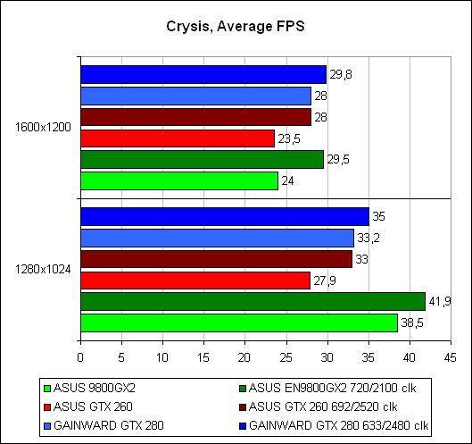
Power Consumption
With a power meter, we could measure the power draw of the entire system and the results below are what we got for the various high-end cards, on Windows Vista running 3DMark Vantage Performance preset. A 1200W Thermaltake PSU was used for this. While our test was unable to isolate the specific power draw of the GeForce GTX 280, the idle power draw of the entire system with that card was lower than all the other cards here, which showed that NVIDIA had indeed improved the dynamic power management on the GTX 280. At peak however, the GTX 280 was as power hungry as the high-end GPUs nowadays and our readings more or less correlate with what we know about this card (236W maximum TDP).
-
Page 1 of 13 — A New Name for a New GenerationPage 2 of 13 — GeForce GTX 200 Architectural Enhancements — Part 1Page 3 of 13 — GeForce GTX 200 Architectural Enhancements — Part 2Page 4 of 13 — The NVIDIA GeForce GTX 280 1GB GDDR3Page 5 of 13 — Test SetupPage 6 of 13 — Win XP Results — 3DMark06 (ver 110)Page 7 of 13 — Win XP Results — Company of Heroes & Unreal Tournament 3Page 8 of 13 — Win XP Results — Crysis (ver 1.1)Page 9 of 13 — Win Vista Results — 3DMark VantagePage 10 of 13 — Win Vista Results — Crysis (ver 1.21)Page 11 of 13 — Temperature and Power ConsumptionPage 12 of 13 — OverclockingPage 13 of 13 — Conclusion
Page 11 of 13 — Temperature and Power Consumption
- Next >
Join HWZ’s Telegram channel here and catch all the latest tech news!
Our articles may contain affiliate links. If you buy through these links, we may earn a small commission.
Retrobenchmarking — GeForce GTX 280 (GT200)
This content has been written by a website visitor and has been rewarded.
Introduction
In the last article devoted to the budget solution NVIDIA GeForce 9600 GT (G94), we noted that in early 2008 the top single-chip ATI/AMD solution represented by the Radeon HD 3870 was already struggling to cope with competition even in the middle- end segment. But with high-end accelerators, the situation for the company was even worse — if in the range from $150 to $300 various versions of the Radeon HD 3850/3870 could compete with NVIDIA products due to constantly decreasing ATI / AMD prices, then those who wanted to get better performance in 3D , albeit sacrificing a wallet, the «red company» had little to offer. Formally, ATI/AMD had dual-processor solutions Radeon HD 3850/3870 X2, the older of which outperformed not only its closest competitor NVIDIA in the face of the updated GeForce 8800 GTS, but also more expensive top-end accelerators GeForce 8800 GTX/Ultra. Here, however, we should not forget that the two-chip solutions lost in terms of power consumption and heat dissipation, and also required significant costs for optimizing drivers and gaming applications in order to avoid performance problems such as poor scalability and the notorious microstatters. And if developers usually did not deprive large AAA projects of attention in terms of optimizations for multi-GPU systems, including dual-chip solutions, then serious problems were observed in not the most popular games. In this situation, ATI/AMD certainly needed to release fundamentally new single-chip accelerators as quickly as possible, but NVIDIA again slightly outstripped the competitor by introducing the new tenth generation of its graphics processors a little earlier, in mid-July 2008. The first accelerators of the new 200th GeForce series were GTX 260 and 280, and today we will talk about the top solution of the new line.
The 2007 update of the architecture of NVIDIA graphics chips can be considered minor — as noted earlier, the new G92 chip was a G80 chip transferred to a 65-nm process technology with minor architectural changes that mainly affected only texture modules. Of course, the transition to a thinner process technology allowed NVIDIA to reduce the cost of chip production and present powerful solutions in the middle price segment, but in 2008 we wanted something truly new. And, I must say, NVIDIA did not disappoint, presenting in June 2008 solutions based on a new video chip code-named GT200, which already implemented a significantly larger number of architectural changes compared to the transition from G80 to G92. Of course, the new chip architecturally differed from its predecessor G80 not as much as the G80 from the G70, but it’s understandable — the unified shader architecture, which proved itself well earlier, was only slightly redesigned and improved. Nevertheless, there were quite serious architectural changes in the GT200 chip, so there is something to talk about.
As we noted in the GeForce 8800 GTX review, NVIDIA’s unified shader architecture chips are an array of devices for floating point calculations, the so-called streaming processors (Streaming Processor, SP). Stream processors are combined into stream multiprocessors (Streaming Multiprocessor, SM), which are independent instruction execution devices containing, in addition to stream processors, more complex devices for calculating transcendental function values and interpolating pixel attributes (Special-Function Unit, SFU), as well as a device fetching and sending execution instructions, a cache of instructions and constants, and a small block of shared memory. Streaming multiprocessors, in turn, are combined into texture-processor clusters (Texture / Processor luster, TPC), equipped with blocks that load data from memory and unload data back into memory.
recommendations
In the G80/G92, each TPC cluster included 2 stream multiprocessors, and each SM stream multiprocessor included 8 SP stream processors and a couple of more complex SFUs. Thus, a full-fledged G80 chip containing 8 TPC clusters boasted 8 × 2 × 8 = 128 stream processors. The G92 chip was designed in the same way, but in the GT200, the internal structure, on the contrary, was significantly changed: firstly, the number of SM streaming multiprocessors per TPC cluster was increased from 2 to 3, and secondly, from 8 to 10 there were the number of TPC clusters in the chip has been increased. As a result, instead of 128 stream processors, a full-fledged GT200 chip already had 10 × 3 × 8 = 240 stream processors, that is, almost twice as many as before! The number of texture units per TPC cluster remained compared to G92 without changes — each TPC had 8 TA texture addressing modules and 8 TF texture filtering modules (in the G80 there were half as many addressing modules). However, due to the increase in the number of TPCs themselves, the total number of texture modules in the GT200 increased from 64 to 80.
Please note that the increase in the number of compute units in the GT200 by an impressive 87.5% was accompanied by only a slight increase in the number of filter modules by 25%. However, this development of NVIDIA’s unified shader architecture is not surprising, as the company was only moving in the direction set by the industry — games used more and more complex shaders from year to year, so performance was no longer limited by texturing speed, as was often the case in the past. .
.
Wide rasterizers, each of which still processed four pixels per clock, also became more — in G80 there were 6 of them, in G92 their number was reduced to 4, and in GT200, on the contrary, increased to 8. Final configuration of the full-fledged GT200 chip, thus, in the format SPs:TMUs:ROPs looked like 240:80:32, while the G80 and G92 had a configuration of 128:32:24 and 128:64:16, respectively.
The changes already described above would be enough to bring 3D accelerators to a new level of performance, even taking into account the fact that the frequencies of the computing units in the GTX 280 were lowered compared to previous solutions due to increased power consumption and heat dissipation of the new one is much more a complex chip produced using the old 65-nm technology. But NVIDIA did not limit itself to just increasing the number of execution units, as can be seen even from a brief comparison of the characteristics in the table above. Immediately striking is an even wider 512-bit memory bus and its volume increased to 1 GB.
But that’s not all, because in addition to the quantitative changes that lie on the surface, NVIDIA has made a lot of smaller microarchitectural optimizations in the GT200, of which at least the following deserve unconditional mention.
- The number of streams processed simultaneously by the chip has been significantly increased. Each SM in the GT200 could schedule up to 1024 threads, so an entire chip with 30 multiprocessors could execute 30,720 threads. In G80/G92, these figures were noticeably more modest — 768 threads per SM multiprocessor and 12288 for the entire chip.
- The register file size of each multiprocessor has been doubled.
- The ability to execute two instructions simultaneously has been significantly improved. The notorious «dual issue MAD+MUL» mode, which we wrote about in detail in a note on the GeForce 8800 GTX, has finally become a reality.
- Support for double precision calculations has been added. The stream processors in the GT200 were still only able to perform operations on single precision numbers (FP32), but each multiprocessor was additionally equipped with a block for double precision calculations, which are so important for various non-graphical calculations.

As a result of many quantitative and qualitative changes, the efficiency of the unified shader architecture in the GT200 has been significantly increased. And in synthetic tests, and what is more important, in real gaming tests, the new top NVIDIA accelerator significantly outperformed single-chip versions of previous years in speed, sometimes up to two times or even more! Below, for example, are summary charts of the results of comparing the performance of the GeForce GTX 280 and GeForce 9800 GTX, which differed from the GeForce 8800 GTS (G92) only slightly higher frequencies.
On average, the GeForce GTX 280 was faster than the GeForce 9800 GTX at launch by 45% in HD and 66% in FHD. Now let’s see how the situation looks after many years (and many versions of Windows and graphics drivers) in the most advanced game projects that supported DX10 accelerators. The GV-N28-1GH-B card from GIGABYTE will help us with this, the rest of the test bench components remained unchanged:
- GIGABYTE Z390 GAMING SLI motherboard.
- Processor i5-9600K slightly overclocked to 4.8 GHz for all 6 cores under inexpensive LSS ID-Cooling AURAFLOW X 360.
- 2×16 GB Ballistix Sport LT RAM (BLS16G4D32AESE) overclocked to 3733 MHz with primary timings 16-20-20-40.
- Windows 10 2004 installed on a WD Blue SN550 SSD, games installed on a Seagate Barracuda 3 TB ST3000DM008 HDD.
The GeForce GTX 280 is a long and heavy card with a very complex PCB. Power requirements (2 additional connectors 6-pin + 8-pin, at least 40 A at 12 V power supply lines) and heat dissipation (TDP 236 W) of the card are also rather big. Cooling system similar to GeForce 8800 GTS (G92), only with a slightly larger radiator can conditionally cope even after many years. I say «conditionally», because in the FurMark stress test, the temperature of the GPU, even on an open bench, exceeds 90 ° C. On the one hand, even in stress tests, things did not reach the maximum temperature of 105 ° C, on the other hand, even 90 ° C on an open bench is still very hot.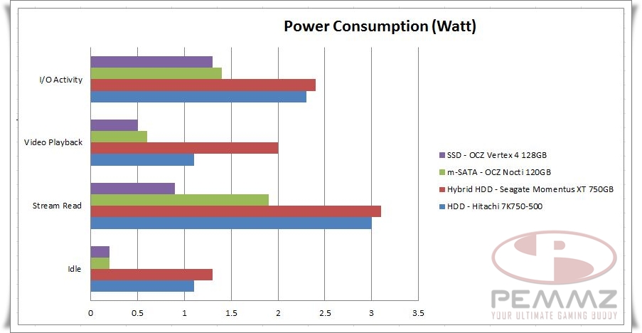 And never quiet. Cooling down the heat of almost one and a half billion transistors is no joke!
Tests
Unigine Tropics
3DMARK Vantage
3DMARK CLOUD GATE
In our set of synthetic tests GTX 280, the total GTS (G9) % in FHD. The GeForce 8800 GTX looks a little more confident in synthetics, so the figures for the superiority of the GeForce GTX 280 over it are slightly less — 55% and 63% in HD and FHD, respectively.
Call of Juarez (Chrome Engine 3, 2007)
Crysis (Cryengine 2, 2007)
Far Cry 2 (Dunia Engine, 2008)
S.T.A.L.K.E.R. Call of Pripyat (X-Ray Engine 1.6, 2009)
Metro 2033 (4a Engine, 2010)
Total War Shogun 2 (TW Engine 3, 2011)
000
9000 9000 Elite V2 (Asura Eingine, 2012)
Hitman Absolution (Glacier 2, 2012)
BIOSHOCK Infinite (Unreal Engine 3, 2013)
Tomb (Crystal Engine, 2013) 9000 9000 9000 9000 9000 9000 9000 9000 9000 9000 9000 9000 9000 9000 9000 9000 9000 9000 9000 9000 9000 9000 9000 9000 9000 9000 9000 2014)
Grand Theft Auto V (Rage, 2015)
Medium -geometric results
GEFORCE GTX 280 above the previous tops of NVIDI 8800 GTS (G92) the new product outperforms the GeForce 8800 GTX by 27–45% and 45–100% in HD and FHD resolutions, respectively, while the advantage over GeForce 8800 GTX in the same resolutions was 36–50% and 50–67%.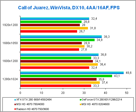
Conclusions
- NVIDIA’s new top single-chip solution turned out to be very powerful, outperforming the previous single-chip accelerators from this company by 1.5–2 times in high (at the time of release) resolutions. If the G92 compared to the G80 gave almost the same performance for less money, that is, it became a breakthrough in terms of price / performance, then the GT200 offered a completely new level of performance, albeit at a price.
- As for the price, then, of course, like any high-end product, the GTX 280, even at a recommended price of $650, could not boast of a good price/performance ratio. But after all, any top-end pieces of iron are not bought for this at all.
- Among other shortcomings, it is worth noting the high power consumption and heat dissipation of the novelty, which led to serious heating (and often the blade of the graphics chip) and a high level of noise in loads.
- The top single-chip product of its rival, the Radeon HD 3870, was hopelessly behind NVIDIA’s new product — in our gaming tests, the GeForce GTX 280 turned out to be faster by 48–96% in HD and 78-150% in FHD.
 ATI/AMD urgently needed to release a worthy single-chip response to the market, since the technological gap between the competitor’s solutions had already become simply colossal.
 - Yes, ATI/AMD, as well as NVIDIA itself, had dual-chip accelerators in its arsenal that could compete with the GeForce GTX 280 in terms of performance and cost less, however, as we have already noted, dual-chip solutions often lost in terms of power consumption and heat dissipation, as well as not always scaling well and suffering from microstatters.
Previous Reviews
- GeForce 8800 GTX (G80)
- GeForce 8800 GTS (G80)
- Radeon HD 2900XT (R600)
- GeForce 8800 GT (G92)
- GeForce 8800 GTS Core 112 (G80)
- Radeon HD 3870 (RV670)
- GeForce 8800 GTS (G92)
- GeForce 9600 GT (G94)
This material was written by a site visitor and has been rewarded.
NVIDIA GeForce GTX 280 Specifications
Home / Video card / Nvidia / Nvidia GeForce GTX 280
- 2 General information
- Memory
The price-quality ratio 13. 8 %
8 %
,0003 649 649 $ / $) $ / rub)
Core clock 1296 MHz
Process technology 65 nm
Power consumption (TDP) 236 W
Maximum memory 1 GB
04
NVIDIA GeForce GTX 280 was released in 2008 and by 2022 it has good performance (better than 53% of all video cards).
The main advantages of this model are: Value for money: 13.8, Price at the time of release: 649, Core frequency: 1296, Technological process: 65, Power consumption (TDP): 236, Maximum memory: 1.
General information
|
Value for money The sum of all the advantages of the device divided by its price. The more%, the better the quality per unit price in comparison with all analogues. |
13.8%
525 place in the rating Price/Quality |
|
Architecture |
Tesla 2. 0 0 |
|
Codename |
GT200 |
|
Type |
Desktop |
|
Release price |
649 $ |
|
Number of shader processors |
240 |
|
Number of CUDA cores A large number of CUDA cores improve performance in graphics computing, |
240 |
|
Core clock |
1296 MHz |
|
Number of transistors |
1.400 million |
|
Process |
65 nm |
|
Power Demand (TDP) |
236 W |
|
Maximum temperature |
105 °C |
|
Floating point performance |
622. 1 gflops 1 gflops |
|
Interface |
PCIe 2.0 x16 |
|
Length |
26.7 cm |
|
Height |
11.1 cm |
|
Additional power connectors |
6-pin & 8-pin |
|
SLI support |
+ |
|
Video connectors |
HDTVDual Link DVI |
|
Multi-monitor support |
1 |
|
Maximum resolution via VGA |
2048×1536 |
|
Audio input for HDMI |
S/PDIF |
|
3D Vision |
+ |
|
DirectX |
11.1 (10_0) |
|
CUDA The CUDA architecture enables applications that are optimized for |
|
|
Floating point performance |
622. 1 gflops 1 gflops |
|
Video connectors |
HDTVDual Link DVI |
|
DirectX |
11.1 (10_0) |
Memory
|
Memory type |
GDDR3 |
|
Maximum memory Large video memory allows you to run demanding games with a lot of textures, |
1 GB
597 place in the rating Memory size |
|
Memory bus width The wider the video memory bus, the more data is transferred to the GPU per unit of time and the better performance in demanding games. |
512 bit |
|
Memory frequency A high memory frequency has a positive effect on the speed of a video card with a large amount of data. |
1107 MHz |
|
Memory bandwidth The greater the data transfer bandwidth, the more effective amount of RAM the PC can use. |
