Hynix – The Memory Guy
The single most interesting thing I learned at the 2015 Flash Memory Summit was that 3D NAND doesn’t have a natural limit, after which some other memory type will need to be adopted.
For years SanDisk has been presenting a memory roadmap (this post’s graphic is one rendition) that anticipates a move to ReRAM after 3D NAND has run through its natural life, which was expected to be as little as three generations. This has been backed by the idea that a 3D NAND stack would only be able to reach a certain number of layers before it would encounter difficulties caused by the need to etch a high aspect ratio hole through an increasing number of layers.
The aspect ratio issue is not hard to understand: Let’s assume that the hole in a 24-layer stack has an aspect ratio of 40:1, then a 32-layer hole would have an aspect ratio of about 50:1, and a 64-layer stack would be something close to 100:1. Today’s technology starts to have trouble etching holes with an aspect ratio higher than 60:1.
These high aspect ratios were thought to be the limiting factor that would prevent 3D NAND from continuing for more than three generations. 3D NAND could only have as many layers as the aspect ratio could support.
On a panel that I moderated at this year’s Flash Memory Summit one panelist, Dr. Myoung Kwan Cho of SK hynix, explained that although there is a limit Continue reading “Flash Memory Summit: Limitless Layers of 3D NAND”
Author Jim HandyPosted on Categories NAND Flash, Vertical StructuresTags aspect ratio, back-grind, backgrind, BiCS, Etch, etching, Hynix, MK Cho, Myoung Kwan Cho, SanDisk, SK, String stacking, Toshiba9 Comments on Flash Memory Summit: Limitless Layers of 3D NAND
For the past ten months DRAM prices have been undergoing a steady slide. Is the market in a crisis? Not really!
Today’s low spot price of $4. 30/GB puts us on a par with February 2013, a full two years ago (see chart). DRAM makers have done a lot to reduce their production costs since that time, so their margins this quarter will be much better than they were in the first quarter of 2013.
But we are still a very long way from the bottom of the last market downturn. In late 2012 spot prices reached a low of $2.52/GB, a full 41% lower than today’s lowest spot prices.
The Memory Guy models the production costs of leading memory chips, and DRAM manufacturing costs have been decreasing for the past several years at an average annual rate of about 30%. That means that costs today are about half of what they were two years ago, and one third of their level this time in 2012.
So even though today’s Continue reading “DRAM Prices Down, But Not So Bad”
Author Jim HandyPosted on Categories Business Strategies, DRAM, Memory Manufacturers, Price Trends & Forecasts, Supply & DemandTags DRAM, Elpida, Hynix, Micron, Nanya, Powerchip, Prices, Samsung, SK, SK Hynix, Spot Market1 Comment on DRAM Prices Down, But Not So Bad
The following is excerpted from an Objective Analysis Alert sent to our clients on March 26: On March 25 SanDisk and Toshiba announced sampling of their 3D NAND flash technology, a 128Gb (gigabit) 48-layer second-generation product based on the BiCS technology that the companies pioneered in 2007. Pilot production will begin in the second half of 2015 with meaningful production targeted for 2016. This release was issued at the same time that Intel and Micron were briefing the press and analysts for their March 26 announcement of their own 3D NAND offering (pictured), which is currently sampling with select customers, and is to enter full production by year-end. The Micron-Intel chip is a 32-layer 256Gb device, which the companies proudly point out is the densest flash chip in the industry.
Similarities and Differences
These two joint ventures (Intel-Micron and SanDisk-Toshiba) are taking very different Continue reading “Four New Players Join 3D NAND Market”
Author Jim HandyPosted on Categories NAND Flash, Vertical StructuresTags 3D, Flash Ventures, Hynix, IMFT, Intel, Micron, Samsung, SanDisk, SK Hynix, Toshiba, V-NAND, VNAND3 Comments on Four New Players Join 3D NAND Market
NAND flash is the process leader in memory technology, and this puts it in a very challenging position: It must ramp to high volume production using techniques that have never been tried before.
The graphic for this post (click to enlarge), supplied by ASML, the semiconductor industry’s leading lithography tool supplier, illustrates the challenge of migrating from one process node to the next. Across the bottom, on the X-axis, are representative process nodes ranging from “2D-45”, or two-dimensional (planar) 45nm NAND, to “3D-5x”, or three-dimensional 5xnm NAND. Below these numbers are the year of volume production.
The vertical axis, labeled “Tolerance” represents the minimum Continue reading “Why NAND is So Difficult to Scale”
Author Jim HandyPosted on Categories NAND Flash, Process Geometries & Die Sizes, Vertical StructuresTags 10nm, 16nm, 1Xnm, 20nm, 25nm, 2Xnm, 35nm, 3D NAND, 45nm, ASM, ASML, BiCS, Bit Cost Scaling, Hynix, IMFT, Intel, lithography, Micron, Moore’s Law, multi pattern, multi patterning, multipattern, multipatterning, patterning, pitch double, pitch doubling, Samsung, SanDisk, SK, Toshiba, V-NAND, vertical NAND, VNAND
Every so often something very strange happens that puzzles The Memory Guy. On December 29 (or Dec. 30 in Seoul) something odd occurred.
I received two e-mails, one from SK hynix at 3:55 PM Pacific Time, and one from Samsung exactly one hour later. Both were press releases.
The SK hynix release was titled: “SK Hynix Developed the World’s First Next Generation Mobile Memory LPDDR4”. It announced that the company is sampling its 20nm-class 8Gb LPDDR4 DRAM to customers.
The Samsung release was Continue reading “Did SK hynix Beat Samsung to the 8Gb LPDDR4?”
Author Jim HandyPosted on Categories DRAM, Memory ManufacturersTags 20nm, 8Gb, Hynix, LPDDR, LPDDR4, Micron, Samsung, SK1 Comment on Did SK hynix Beat Samsung to the 8Gb LPDDR4?
This series has looked at 3D NAND technology in a good deal of technical depth. The last question to be answered centers around the players and the timing of the technology. A lot has been said about the technology and its necessity. Will everyone be making 3D NAND? When will this big transition occur?
This post will provide an update as of its publication (13 December 2013) to show each company’s current status, to the best of The Memory Guy’s understanding./fddfe1f8b92a77f.s.siteapi.org/img/90a25c54d70f3af6abe33f1c48529aa2cc742d52.jpg) Readers may want to refer back to the earlier posts in this series, as well as to a June 2013 Nikkei TechON article that gives a good review of the 3D NAND alternatives that have been presented at various technical conferences.
Readers may want to refer back to the earlier posts in this series, as well as to a June 2013 Nikkei TechON article that gives a good review of the 3D NAND alternatives that have been presented at various technical conferences.
Let’s start with Samsung, the largest producer of NAND flash today. Just prior to Memcon 2013 last Continue reading “3D NAND: Who Will Make It and When?”
Author Jim HandyPosted on Categories Memory Manufacturers, NAND Flash, Vertical StructuresTags 3D NAND, 3DNAND, BiCS, cake, Charge Trap, Cheese, hole, Hynix, IEEE, IMFT, Intel, Intel Micron Flash Technology, layer cake, Macaroni, Micron, nitride, ONO, Samsung, SanDisk, Schiltron, SK Hynix, slit, SONOS, TANOS, TCAT, Toshiba, Transactions, trench, V-NAND, Walker4 Comments on 3D NAND: Who Will Make It and When?
The following is excerpted from an Objective Analysis Alert that can be downloaded from the company’s website.Rambus and Micron announced on Tuesday that they have signed a patent cross license agreement. Micron receives rights to Rambus IC patents, including memories. Both Micron and Elpida products will be covered. The companies have thus settled all outstanding patent and antitrust claims in their 13-year court battle.
Micron will make royalty payments to Rambus of up to $10 million per quarter over the next seven years, totaling $280 million, after which Micron will receive a perpetual, paid-up license.
Rambus and Micron both have Continue reading “Rambus and Micron Sign License Agreement”
Author Jim HandyPosted on Categories DRAM, Memory Interfaces, Memory ManufacturersTags Elpida, Hynix, IP, Micron, NEC, patents, Qimonda, R-DRAM, Rambus, Samsung
Some of my readers have asked: “How is 3D NAND programmed and erased? Is it any different from planar NAND?”
In a word: No.
(Before I get too far into this allow me to admit that The Memory Guy doesn’t understand quantum physics, so I will be presenting this only to the depth that I understand it. There will be no band-gap diagrams or equations to wrestle with.)
Both 3D NAND and planar NAND use Fowler Nordheim Tunneling (FN) to both program and erase. This differs from NOR flash which programs bits using Continue reading “How Do You Erase and Program 3D NAND?”
Author Jim HandyPosted on Categories Charge Trapping, NAND Flash, Vertical StructuresTags BiCS, Bit Cost Scaling, Channel Hot Electron, Charge Trap, charge trapping, CHE, CTF, FN, Fowler Nordheim, Hot Hole Injection, Hot-Electron Injection, Hynix, IMFT, Intel, Micron, ONO, Samsung, SanDisk, SONOS, Spansion, TANOS, TCAT, Terabit Cell Array Transistor, Toshiba, Tunneling, V-NAND, VNAND6 Comments on How Do You Erase and Program 3D NAND?
One of the thornier problems in making 3D NAND is the job of connecting the peripheral logic (the row decoders) to all of those control gates that are on layers buried somewhere within the bit array. Remember that the control gates are the conductive sheets of polysilicon or tantalum nitride at various depths in the chip.
The problem boils down to this: You can’t run connections from each layer up or down the side of the chip to get to the CMOS circuits below. Instead you have to create a terrace structure to expose and connect to each layer.
These connections are made by etching a stair-step pattern into the layers and sinking Continue reading “3D NAND: How do You Access the Control Gates?”
Author Jim HandyPosted on Categories NAND Flash, Technical Trends, Vertical StructuresTags 3D NAND, 3DNAND, BiCS, Bit Cost Scaling, Hynix, IEDM, IEEE, IMFT, Intel, Micron, NAND Flash, oxide, pillar, poly, polysilicon, Samsung, silicon dioxide, slit, Stair Case, Stair Step, Staircase, Stairstep, TCAT, Toshiba, Tower, V-NAND, Vertical Structures, VLSI Technology Forum, VLSIT, VNAND, word lines, wordlines6 Comments on 3D NAND: How do You Access the Control Gates?
My prior 3D NAND post explained how Toshiba’s BiCS cell works, using a silicon nitride charge trap to substitute for a floating gate. This post will look at an alternative technology used by Samsung and Hynix which is illustrated in the first graphic, a diagram Samsung presented at a technical conference. This cell also uses a charge trap.
Let The Memory Guy warn you, if the process in my prior post seemed tricky, this one promises to put that one to shame!
Part of this stems from the use of a different kind of NAND bit cell. You can shrink flash cells smaller if you use a high-k gate dielectric (one with a high dielectric constant “k”) since it Continue reading “An Alternative Kind of Vertical 3D NAND String”
Author Jim HandyPosted on Categories NAND Flash, Vertical StructuresTags 2009, 3D NAND, 3DNAND, Alumina, BiCS, Bit Cost Scaling, cake, Charge Trap, charge trapping, column, CTF, floating gate, frosting, gate-all-around, hole, Hynix, IBM, IEDM, IEEE, IMFT, Intel, layer cake, Micron, NAND Flash, nitride, ONO, oxide, pillar, poly, polysilicon, Samsung, silicon dioxide, silicon nitride, slit, TANOS, Tantalum, TFT, Toshiba, Tower, trench, trench cell, tube, V-NAND, Vertical Structures, VLSI Technology Forum, VLSIT, VNAND, word lines, wordlines17 Comments on An Alternative Kind of Vertical 3D NAND String
20nm – The Memory Guy
In a November 25 press release Samsung introduced a 128GB DDR4 DIMM. This is eight times the density of the largest broadly-available DIMM and rivals the full capacity of mainstream SSDs.
Naturally, the first question is: “How do they do that?”
To get all the chips into the DIMM format Samsung uses TSV interconnects on the DRAMs. The module’s 36 DRAM packages each contain four 8Gb (1GB) chips, resulting in 144 DRAM chips squeezed into a standard DIMM format. Each package also includes a data buffer chip, making the stack very closely resemble either the High-Bandwidth Memory (HBM) or the Hybrid Memory Cube (HMC).
Since these 36 packages (or worse, 144 DRAM chips) would overload the processor’s address bus, the DIMM uses an RDIMM protocol – the address and control pins are buffered on the DIMM before they reach the DRAM chips, cutting the processor bus loading by an order of magnitude or more. RDIMMs are supported by certain server platforms.
The Memory Guy asked Samsung whether Continue reading “Samsung’s Colossal 128GB DIMM”
Author Jim HandyPosted on Categories DRAM, Memory Interfaces, Memory Manufacturers, Memory Packaging, Packaging AdvancesTags 128 Gigabyte, 128Gb, 20nm, 8Gb, HBM, High-bandwidth Memory, HMC, Hybrid Memory Cube, Samsung8 Comments on Samsung’s Colossal 128GB DIMM
NAND flash is the process leader in memory technology, and this puts it in a very challenging position: It must ramp to high volume production using techniques that have never been tried before.
The graphic for this post (click to enlarge), supplied by ASML, the semiconductor industry’s leading lithography tool supplier, illustrates the challenge of migrating from one process node to the next. Across the bottom, on the X-axis, are representative process nodes ranging from “2D-45”, or two-dimensional (planar) 45nm NAND, to “3D-5x”, or three-dimensional 5xnm NAND. Below these numbers are the year of volume production.
The vertical axis, labeled “Tolerance” represents the minimum Continue reading “Why NAND is So Difficult to Scale”
Author Jim HandyPosted on Categories NAND Flash, Process Geometries & Die Sizes, Vertical StructuresTags 10nm, 16nm, 1Xnm, 20nm, 25nm, 2Xnm, 35nm, 3D NAND, 45nm, ASM, ASML, BiCS, Bit Cost Scaling, Hynix, IMFT, Intel, lithography, Micron, Moore’s Law, multi pattern, multi patterning, multipattern, multipatterning, patterning, pitch double, pitch doubling, Samsung, SanDisk, SK, Toshiba, V-NAND, vertical NAND, VNAND
Every so often something very strange happens that puzzles The Memory Guy. On December 29 (or Dec. 30 in Seoul) something odd occurred.
I received two e-mails, one from SK hynix at 3:55 PM Pacific Time, and one from Samsung exactly one hour later. Both were press releases.
The SK hynix release was titled: “SK Hynix Developed the World’s First Next Generation Mobile Memory LPDDR4”. It announced that the company is sampling its 20nm-class 8Gb LPDDR4 DRAM to customers.
The Samsung release was Continue reading “Did SK hynix Beat Samsung to the 8Gb LPDDR4?”
Author Jim HandyPosted on Categories DRAM, Memory ManufacturersTags 20nm, 8Gb, Hynix, LPDDR, LPDDR4, Micron, Samsung, SK1 Comment on Did SK hynix Beat Samsung to the 8Gb LPDDR4?
Micron has announced that it is sampling a new 128Gb NAND flash chip based upon a 16nm process, with production slated for the fourth quarter. To The Memory Guy’s knowledge this is the tightest process available.
The company, with its partner Intel, gained a lead with its 20nm process generation through its use of a Hi-k tunnel dielectric, a new material that replaces more conventional silicon dioxide layer with a new material (Micron won’t say what) that yields the same capacitance with a thinner layer. This has become very important with today’s tight processes because of issues of inter-cell interference.
Other NAND makers are migrating to Continue reading “Micron NAND Reaches 16nm”
Author Jim HandyPosted on Categories Memory Manufacturers, NAND FlashTags $/GB, 16nm, 20nm, 22nm, 27nm, cost, die size, dielectric, Hi-k, high k, Intel, Micron, NAND, Samsung, SanDisk, silicon dioxide, SK Hynix, Toshiba1 Comment on Micron NAND Reaches 16nm
SanDisk and Toshiba, in separate announcements, both today disclosed their next-generation process technology.
The companies introduced their new “1y” processing node that, according to SanDisk, produces 19nm x 19.5nm cell, versus the earlier “19nm” process (or “1x”) that used a 19nm x 26nm cell.
The graphic for this post (click to enlarge) was presented during SanDisk’s May 5th Analyst Day and compares the 24nm process to the 19 x 26nm process, moving to the 19 x 19nm process, and eventually to “1z” which neither company is yet revealing. After the 1z process SanDisk believes Continue reading “SanDisk & Toshiba Move to Next Process Node”
Author Jim HandyPosted on Categories NAND Flash, Technical TrendsTags 19nm, 20nm, 24nm, dielectric, Hi-k, high k, IMFT, Intel, Micron, NAND Flash, process technology, Samsung, SanDisk, Toshiba1 Comment on SanDisk & Toshiba Move to Next Process Node
Micron Technology and Intel announced today (6 December, 2011) that the two companies are sampling a 128 gigabit (that’s 16 gigabytes) NAND flash chip manufactured by the company’s IMFT joint venture.
This is a doubling of the capacity of the 64Gb chip the companies announced in April, but they assure us that the size of the die hasn’t doubled, and the accompanying photo supports this. Intel tells us that the die will fit into standard BGA and TSOP packages. Continue reading “Micron, Intel, Introduce 128Gb NAND Chip”
Author Jim HandyPosted on Categories Memory Manufacturers, NAND Flash, Process Geometries & Die SizesTags 20nm, flash, IMFT, Intel, Micron, Micron Technology, NAND, ONFi, semiconductors
Comparison 1Y nanometer NAND architecture and beyond
By Jeongdong Choe, PhD. , TechInsights
A few years ago, some of the semiconductor process and device analysts thought 2D planar NAND Flash would soon be coming to an end due to the scaling limits, especially around the 20nm or sub-20nm generation. Do we still think the 2D NAND Flash technologies have hit the scaling wall? According to TechInsights’ deep-dive analysis on current and future NAND Flash technologies, although 3D V-NAND architecture could help with the scaling limit, we believe the 2D MLC and TLC NAND Flash technologies remain strong and cost effective for 14nm, 12nm and even for single-digit nanometer node.
When it comes to 3D NAND technology, Samsung has been developing and mass-producing 32-tier V-NAND architecture (for technical analysis related to the Samsung 3D V-NAND click here) with MLC and TLC for their 850 PRO and 850 EVO since 2014, although, this is not the final goal for Samsung due to a relatively low yield, process complexity and bit-cost viewpoints. More 3D Flash products may appear at the end of this year, or early in 2016, as major NAND players such as Toshiba, SanDisk, Micron, Intel, and SK-Hynix bring out their 3D products with 24-tier, 32-tier or 48-tier FG (floating gate)/CTF (charge-trap-flash) architecture (Figure 1).
Figure 1. 2D and 3D NAND Technology Roadmap (Source: TechInsights Nand Roadmap, download here)
However, the ultimate target for 3D NAND is 128-tier or at least 64-tier structure from the bit-cost viewpoints. In that case, the aspect ratio of Si-channel and common source contacts would be over 80:1, which is a strong burden for process integration engineers. In addition, the uniformity of the 64-tier or 128-tier NAND cell characteristics in a NAND string and their endurance/retention/reliability properties during program/erase operation would be another big challenge for the vertical NAND string architecture.
The scaling limits for 10 nm-class and sub-10 nm 2D planar NAND structures include patterning technology including QPT (Quadruple Patterning Technology), cell-to-cell interference such as cross-talk, poly-Si gap-filling process for control gate (CG), self-aligned STI (SA-STI) for isolation patterning, self-aligned process (SAP) for CG/FG, interconnection methodology including pad layout/design, inter-poly dielectric (IPD) layer engineering, and cell transistor channel/source-drain (S/D) engineering. According to TechInsights’ detailed structural analysis and comparison of 15nm and 16nm NAND flash devices (so called 1Y NAND technology node) such as Samsung 16nm, Toshiba 15nm, Micron 16nm and SK-Hynix 16nm products, we may expect that at least two more next generation 2D planar NAND products having 12nm and less than 12 nm technology would be developed and released from major players near future. As for NAND memory density and die size, Toshiba/SanDisk 15nm TLC products have 1.28 Gb/mm2 which is double from other MLC products although Samsung 32-tier 3D V-NAND TLC products have 1.87 Gb/mm2 (Figure 2).
Figure 2. Comparison of NAND memory density for each product (Source: TechInsights)
For patterning the three finest lines of the NAND cell structure such as active/STI, gate/wordline (CG/FG) and bitline (usually, metal-2 lines), a quadruple patterning technology (QPT) seems to be very mature for each of the major NAND players. They use their own QPT integration on three critical layers with three or four masks, SOH etching and two-step self-align reverse patterning (SARP) process. Although the critical dimensions have a little skew on every four patterns, they have successfully developed QPT integration with less than 1nm CD (Critical Dimension) and it could be extended into 10nm and even single-digit nanometer NAND products. Fortunately and thanks to state-of-the-art anisotropic plasma etching and ALD/CVD technology, uniformly repeated 8nm patterns would be possible for NAND cell array. Figure 3 shows a comparison of DPT/QPT patterns for each product.
Figure 3. Comparison of DPT and QPT patterns for each product (Source: TechInsights)
Micron uses a 3.3nm thin-FG poly-Si storage node to decrease cell-to-cell interference, while other manufacturers introduce an air-gap process for active, gate wordline (FG/CG) and bitline (metal-2) for thick-FG structure. Especially, the air-gap process has been developed and applied on the channel region of active patterns and FG/CG pillars help decrease the cross-talk.
For an IPD (Inter-Poly Dielectric) or a barrier layer between CG and FG, a multi-layer stacked with thin oxide (O) and nitride (N) layers such as ONO or NONON structure has been used for mid-10 nm class NAND devices, while Micron uses a high-k dielectrics such as HfO/SiO/HfO/Nitrided-SiO which is the same as their 20 nm NAND products. Micron successfully integrated IPD/FG/Tunnel-oxide and decreased FG thickness from 5 nm to 3.3 nm with high-k IPD. It might be further reduced to 10ish nm NAND products by optimizing IPD/FG quantum well structure for their unique thin-FG architecture. A 6 nm tunnel oxide (SiO) is used on Micron, Toshiba/SanDisk and SK-Hynix, while Samsung uses nitrogen-doped oxide in its top and bottom portion.
Triple-row staggered bitline contacts (BC) are used on Toshiba/SanDisk for the first time which is an excellent choice to make things smooth for cell layout and process integration although NAND string overhead is increased from 13% to 19%. Other players still use double-row staggered BC layouts on their 15nm/16nm NAND products (Figure 4).
Figure 4. Double- and triple-row staggered bitline contacts (Source: TechInsights)
Other barriers to extend 2D planar NAND to 10nm such as CG poly fill-ability, anisotropic etching for SA-FG/STI and CG/FG, cell transistor S/D engineering and leaning effect during the process integration are still there. Nevertheless, major players and their equipment vendors will successfully develop and integrate the 10 nm 2D NAND architecture in a few years.
I believe most of the major NAND players have their own matured process integration capability with assistance from ECC and circuit/layout optimization. 2D NAND technology will be further scaled down to 12nm, 10nm, or even 8ish nm which is more cost-effective than 3D V-NAND for near future NAND products.
Jeongdong Choe has more than 20 years of experience on semiconductor process and device integration including NAND Flash, DRAM, logic and advanced memory devices at Samsung and SK-Hynix. He works at TechInsights as a consulting engineer especially focusing on memory and logic process integration.
Easily post a comment below using your Linkedin, Twitter, Google or Facebook account. Comments won’t automatically be posted to your social media accounts unless you select to share.
Flash memory chips: thinner and denser
-
Market
-
Business
home
12/12/2013Author
Evgeny Kuryshev
SK Hynix, a manufacturer of DRAM and NAND memory chips, announced the start of mass production of MLC (Multi Level Cell) NAND flash memory with a density of 64 Gb using a 16 nm process technology.
SK Hynix, manufacturer of DRAM and NAND memory chips, announced the start of mass production of MLC (Multi Level Cell) NAND flash memory with a density of 64 Gb using a 16 nm process technology.
The company’s management is interested in maintaining the competitiveness of its products: the mass production of the first version of 16nm NAND flash memory started back in June. And today, at the end of the year, SK Hynix introduced the second generation of 16 nm MLC NAND chips with a density of 64 Gbit, which should become more profitable due to the next miniaturization of the chip. The Koreans officially claim that we are talking about the most delicate manufacturing process in the industry.
Here it is worth noting that the thinner the technical process, the more often and more strongly neighboring cells of the chip interfere with each other. To reduce the impact of these interferences, instead of the usual insulating materials, SK Hynix engineers use Air-Gap technology, which organizes insulating shields using the so-called vacuum holes.
But that’s not all. A similar MLC NAND flash memory chip has already been developed with a density of 128 Gb (which corresponds to a capacity of 16 GB), built according to the same technical specification as the younger, 64 Gb version. This is claimed to be the highest density for a single MLC chip to date. This type of memory will be launched in early 2014.
SK Hynix also confirmed its intention to develop alternative technologies for the NAND flash segment, such as TLC (Triple Level Cell) and 3D NAND.
IT-News magazine [№ 17/2013 (December 30)] Journal subscription
Technologies
Previous
IT transformation — Dmitry Pshychenko
Next
NAND-chip market: conscious limitations
Want to be the first to know about new materials?
Subscribe to the newsletter
Weekly
Material Tape
By clicking on the button, I accept the terms of the agreement.
Related Articles
New tablet form factor from Samsung and Intel
Samsung Display and Intel are working on «sliding» PCs. Yesterday, a prototype was shown that transforms from a 13-inch tablet to a 17-inch display…0053
Now there are 173 high-tech development zones in China, and about 50 more are planned to be created by 2030. It is expected that this will lead to an increase in in September
It is expected that after the completion of technology research and development, mass production of chips using the production process N3 …
TSMCTechnology, 18.08.22
The future of supersonic passenger aviation.
American Airlines has confirmed the purchase of twenty Boom Supersonic Overture supersonic passenger aircraft. They can carry the passage…
Technologies, 17.08.22
Load more1
2
3
four
5
»»
Next →
20:52
Apple forced to accept price increase for TSMC chips
20:35
ITentika: creating solutions that allow customers to increase profits
20:03
Mavic 3 Enterprise and Mavic 3 Thermal drones in Russia
16:49
GoodWAN temperature and humidity sensors are available in OCS TOIR»
15:57
Certificates and certificates from the registry office can be ordered at the State Services
15:48
How to train employees: motivation, personal approach and discussion communities
15:42
Optimacrosa
14:09
Google is working on artificial intelligence — the creator of the video
13:29
The government of the Russian Federation will subsidize manufacturers of laptops, computers, tablets
Go to section
Road Show SearchInform 20022: Security in new realities Offline
Date: 20. 09.22 — 22.11.22
18th Mining and Geological Forum and Exhibition MINEX Russia 2022
Offline
Date: 04.10.22 — 06.10.22
Global Information Security Days
Online
Date: 05.10.22-07.10.22
All events
IT-NEWS №
Technological Sports. Politics
Mobilization. How will this affect the IT market?
Experience
Work under sanctions. How Businesses Handle Challenges and Constraints
Video Log
IT Wednesday
IT and Business.
What is important today?
First-hand ideas and opinions
Valery Baulin, Group-IB: “There has been a lot of work”
Parallel import of IT equipment: turbulence will be replaced by adaptation
IB in cloudy conditions. Cyber confrontation
The Merge: the end of the era of mining farms
Multi-factor authentication with MULTIFACTOR: remote work without danger
Dual-loop monetary and financial system of the Russian Federation: the end of dollar hegemony or a return to a planned economy?
IB in conditions of high cloudiness. «Iron» supplies
BI analytics without analytical storage: life hack or mistake?
Russian market of software robots
Video conferencing in Russian
14nm process — SANDBIGBOX.com
12nm, 14nm and 16nm manufacturing units are discussed here.
|
Scaling MOSFET (technology nodes) |
|
|
Future
|
|
The 14 nm process refers to the MOSFET node technology which is the successor to the 22 nm (or 20 nm) node. 14 nm was named as such in the International Technology Roadmap for Semiconductors (ITRS). Until about 2011, the next node after 22 nm was expected to be 16 nm. All 14nm nodes use FinFET (fin field-effect transistor) technology, a type of multi-gate MOSFET technology that is a non-planar evolution of planar silicon CMOS technology.
Samsung Electronics launched a 14nm chip in 2014, and started manufacturing 10nm-class NAND chips in 2013. [ Clarification required ] In the same year, SK Hynix began mass production of 16nm NAND flash and TSMC mass-produced 16nm FinFET. production. The following year, Intel began shipping 14nm devices to consumers.
- 1 History
- 1.1 Prerequisites
- 1.2 Technology Demonstrations
- 1.3 Transport devices
- 2 processes 14 nm
- 3 links
The basis for sub-20nm fabrication is FinFET (FET), an evolution of the MOSFET. [1] FinFET technology was first proposed by Dai Hisamoto and his research team at the Hitachi Central Research Laboratory in 1989. [2] [3]
14 nm resolution is difficult to achieve in polymer resist even with electron beam lithography. In addition, the chemical effects of ionizing radiation also limit reliable resolution to around 30 nm, which is also achievable using modern immersion lithography. Hard masking materials and some patterns are required.
A more significant limitation is associated with plasma damage to materials with low k . The degree of damage is usually 20 nm [4], but can reach up to 100 nm. [5] Damage sensitivity is expected to deteriorate as low k materials become more porous. For comparison: the atomic radius of unrestricted silicon is 0.11 nm. Thus, about 90 Si atoms will span the length of the channel, resulting in significant leakage.
Around 2010, Tela Innovations and Sequoia Design Systems developed a methodology to allow double exposure for the 16/14 nm node. [6] Samsung and Synopsys have also begun implementing dual patterning in the 22 and 16 nm design streams. [7] Mentor Graphics announced that it released 16nm test chips in 2010. [8] On January 17, 2011, IBM announced that they had teamed up with ARM to develop 14 nm chip processing technology. [9]
On February 18, 2011, Intel announced that it would build a new $5 billion semiconductor manufacturing facility in Arizona to manufacture chips using a 14nm process and advanced 300mm wafers. [10] [11] The new production facility was to be called Fab 42 and construction was to start in mid-2011. Intel billed the new facility as «the most advanced high-volume manufacturing facility in the world» and said it would launch in 2013. Intel has since decided to delay the opening of this facility and instead upgrade its existing facilities to support 14nm chips. [12] On May 17, 2011, Intel announced development plans for 2014 that included 14 nm transistors for its Xeon, Core, and Atom product lines. [13]
[13]
In the late 1990s, the Japanese Hisamoto team from Hitachi Central Research Laboratory began collaborating with an international team of researchers to further develop the FinFET technology, including TSMC’s Chenming Hu and various UC Berkeley researchers. In 1998, the team successfully produced devices using the 17nm process. Later in 2001 they developed the 15nm FinFET process. [1] In 2002, an international team of researchers from UC Berkeley including Shibli Ahmed (Bangladesh), Scott Bell, Cyrus Taberi (Iran), Jeffrey Bokor, David Kaiser, Chenming Hu (Taiwan Semiconductor Company) and Tsu -Je Qing Liu, demonstrated FinFET devices with gate lengths up to 10 nm. [1] [14]
In 2005, Toshiba demonstrated a 15nm FinFET process with a gate length of 15nm and a fin width of 10nm using a sidewall padding process. [15] It has been suggested that for a 16 nm node, the logic transistor would have a gate length of about 5 nm. [16] In December 2007, Toshiba demonstrated a prototype memory unit using 15 nanometer thin lines. [17]
In December 2009, the National Nanolaboratory of Nanodevices, owned by the government of Taiwan, produced a 16nm SRAM chip. [18]
In September 2011, Hynix announced the development of 15nm NAND cells. [19]
In December 2012, Samsung Electronics installed a 14nm chip. [20]
In September 2013, Intel demonstrated an Ultrabook laptop with a 14nm Broadwell processor, and Intel CEO Brian Krzanich said, «[CPUs] will be on sale by the end of this year.» [21] However, the shipment was delayed until the fourth quarter of 2014. [22]
In August 2014, Intel announced details of the 14nm microarchitecture for its upcoming Core M processors, the first product to be manufactured on Intel’s 14nm manufacturing process. According to a press release, the first systems based on the Core M processor were expected to arrive in the fourth quarter of 2014. «Intel’s 14nm technology uses second-generation three-gate transistors to provide industry-leading transistor performance, power, density, and cost,» said Mark Bohr, Intel senior fellow, technology and manufacturing group, and director of process architecture and integration. [23]
In 2018, Intel announced a shortage of 14nm manufacturing capacity. [24]
In 2013, Hynix IC started mass production of 16nm NAND flash, [25] TSMC started 16nm FinFET production, [26] and Samsung started 10nm class NAND flash production. [27]
On September 5, 2014, Intel released the first three Broadwell-based processors that belonged to the low TDP Core M family: Core M-5Y10, Core M-5Y10a, and Core M-5Y70. [28]
In February 2015, Samsung announced that its flagship Galaxy S6 and S6 Edge smartphones will feature 14nm Exynos SoCs. [29]
March 9, 2015 Apple Inc. released the «Early 2015» MacBook and MacBook Pro, which used 14nm Intel processors.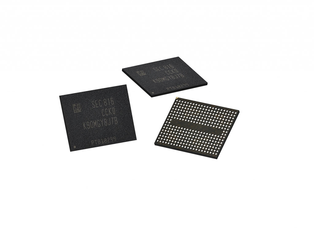 Of note is the i7-5557U with Intel Iris Graphics 6100 and two cores running at 3.1 GHz, consuming only 28 watts. [30] [31]
September 25, 2015 Apple Inc. released the iPhone 6S and iPhone 6S Plus, which are equipped with «desktop grade» A9 chips [32] , which are manufactured in both Samsung’s 14nm process and TSMC’s (Taiwan Semiconductor Manufacturing Company) 16nm process.
In May 2016, Nvidia released its GeForce 10 series GPUs based on the Pascal architecture, which includes TSMC’s 16 nm FinFET technology and Samsung’s 14 nm FinFET technology. [33] [34]
In June 2016, AMD released its Radeon RX 400 GPUs based on the Polaris architecture, which incorporates Samsung’s 14nm FinFET technology. The technology has been licensed by GlobalFoundries to use dual providers. [35]
On August 2, 2016, Microsoft released the Xbox One S, in which TSMC used 16 nm.
On March 2, 2017, AMD released its Ryzen processors based on the Zen architecture, incorporating Samsung’s 14nm FinFET technology licensed by GlobalFoundries from GlobalFoundries. [36]
[36]
The NEC SX-Aurora TSUBASA processor, introduced in October 2017 [37], uses TSMC’s 16 nm FinFET process and is designed for use with NEC SX supercomputers. [38]
On July 22, 2018, GlobalFoundries announced a 12nm Leading-Performance (12LP) process based on Samsung’s licensed 14LP process. [39]
In September 2018, Nvidia released GPUs based on its Turing microarchitecture, which were manufactured in TSMC’s 12nm process and have a transistor density of 24.67 million transistors per square millimeter. [40]
| Basic Rules ITRS Logic Device (2015) |
[a] | TSMC | Intel | GlobalFoundries [b] | SMIK | |
|---|---|---|---|---|---|---|
| Process name | ~ 16/14 nm | ~ 14 nm | ~ 16/12 nm | ~ 14 nm | 14 nm, 12 nm [41] | 14 nm |
| Transistor Density (MTr/mm²) | Unknown | 32. 94 [39] 94 [39] |
28.88 [42] | 37.5 [43] [c] | 36.71 [39] | ? |
| Transistor gate pitch | ~ 70 nm | ~ 78nm — 14LPE (HD) ~ 78nm — 14LPP (HD) ~ 84nm — 14LPP (UHP) ~ 84nm — 14LPP (HP) |
~ 88 nm | ~ 70 nm (14 nm) 70 nm (14 nm +) 84 nm (14 nm ++) |
84 | ? |
| Interconnect pitch | ~ 56 nm | ~ 67 nm | ~ 70 nm | ~ 52 nm | ? | ? |
| Transistor fin pitch | ~ 42 nm | ~ 49 nm | ~ 45 nm | ~ 42 nm | 48 | ? |
| Transistor fin width | ~ 0 8 nm | ~ 0 8 nm | Unknown 9 Richard, O.; and others. (2007). «Sidewall damage in the basis of silicon dioxide with low K material caused by various patterning of plasma processes, studied energy scanned and analytical TMI».  Microelectronic engineering . 84 (3): 517–523. Gross, T.; and others. (2008). «Detection of nanoscale etching and ash damage of nanoporous methylsilsesquioxane using electrostatic force microscopy». Microelectronic engineering . 85 (2): 401–407. DOI : 10.1016 / j.mee.2007.07.014 . Microelectronic engineering . 84 (3): 517–523. Gross, T.; and others. (2008). «Detection of nanoscale etching and ash damage of nanoporous methylsilsesquioxane using electrostatic force microscopy». Microelectronic engineering . 85 (2): 401–407. DOI : 10.1016 / j.mee.2007.07.014 .
9 Axelrad, V.; and others. (2010). Rieger, Michael L; Thiele, Jörg (ed.). «16 nm with 193 nm immersion lithography and double exposure». Proc. SPY . Design for manufacturability through design and process integration IV. 7641 : 764109. DOI : 10.1117 / 12.846677 . Hello friends! A regular reader of ours asked a good question the other day. He asked how to find out how much longer his SSD will last or how to find out the working life of his SSD. Also last week, other users asked more questions on this topic, for example: Which type of flash memory is better for SSD: NAND, 3D NAND, 3D V-NAND and NOR? How can I find out which memory chips the purchased SSD (SLC, MLC or TLC) consists of and which memory is better? What is the number of overwrite cycles or TBW? We will answer all these interesting questions in today’s article. Author Vladimir! I’m not afraid to repeat myself and say that everything is important in a computer, including a solid-state drive. The performance and life of an SSD depends on two terms — the type of NAND flash memory chips: (SLC, MLC, TLC) and the controller with firmware. The price of the drive directly depends on them. There are two main types of Flash memory in SSDs: NOR and NAND . NAND technology is faster and cheaper. NAND memory has been improved to date. 3D NAND and 3D V-NAND memory appeared. If we take the market of SSDs currently offered on the market, then 5 percent belongs to 3D V-NAND, 15 percent to 3D NAND, and the remaining 80 percent to NAND. These data with an error, but small. In turn, Flash memory: NAND can have three types of memory chips: SLC, MLC and TLC. To date, SSDs based on MLC and TLC flash memory are mainly sold. According to TLC and MLC, the SSDs offered on the market are 50 to 50. TLC memory has a lower TBW limit. The AIDA64 program can show the type of SSD memory, the official website of the developer https://www.aida64.com/ In the main window of the program, select «Data storage», then select the SSD model, for example, I have three SSDs installed in the system and I will choose the first one — Samsung 850 Evo 250GB. As you can see, the flash memory type of the drive is TLC. Second Kingston SHSS37A/240G flash type MLC. How to find out the resource of a solid state driveFor example, let’s find out the resource of Kingston SHSS37A/240G. Go to the official website of the device manufacturer https://www.hyperxgaming.com/ru Select «Solid State Drives» —> «Savage». Capacity 240 GB and we see the total amount of data (TBW) that can be written to the Kingston SHSS37A drive with a capacity of 240 GB — 306 TB. Let’s compare it with Samsung 850 Evo 250GB drive. We go to the official website of the manufacturer http://www.samsung.com/ru/ssd/all-ssd/ We mark the item — Drive SSD 850 Evo Sata III. Capacity 240 GB and left-click on the image of the SSD. «Show all characteristics» We see the indicator at the very bottom. Recording resource: 75 TB. It turns out that the Kingston SHSS37A / 240G SSD has a TBW rewrite cycle resource four times larger. If you have an OCZ SSD, then go to the website https://ocz.com/us/ssd/ 0053To do this, we will use the CrystalDiskInfo program. In the main window of the program, select my Samsung 850 Evo 250GB SSD. In the item «Total host records» we see the amount of data written to the drive 41.088 TB. If we compare this figure with the Recording resource indicated on the official website: 75 TB, then we can conclude that 33 TB of data can still be written to the SSD. In the case of Kingston SHSS37A/240G SSD, CrystalDiskInfo cannot show the total amount of data written to the drive. In this case, we will use the SSD — Z program. In the main window, in the “Bytes Written” item, we see the amount of data written to the drive 43,902 TB. If we compare this figure with the Recording resource indicated on the official website: 306 TB, then we can conclude that 262 TB of data can still be written to the SSD. |
 9 But, MS .; and others. (2010). Dusa, Mircea V; Conley, Will (ed.). «Introduction and validation of dual patterning in product and pattern design processes from 22 to 16 nm.» Proc. SPY . Optical microlithography XXIII. 7640 : 76400S. Bibcode : 2010SPIE.7640E..0SN 9 Ahmed, Shibli; Bell, Scott; Tabery, Cyrus; Bokor, Geoffrey; Kaiser, David; Hu, Chenmin; Liu, Tsu-Je King; Yu, Bin; Chang, Leland (December 2002). FinFET scaling to 10 nm gate length (PDF) . Digest. International Conference on Electronic Devices : 251–254.
 9 Kaneko, A; Yagashita, A; Yahashi, K; Kubota, T; and others. (2005). «Sidewall transfer process and technology for forming selective gate sidewall separators for FinFET less than 15 nm thick with increased source/drain extension.» IEEE International Electron Devices Meeting (IEDM 2005) . pp. 844–847. 9 «Samsung Mass Production 128GB 3-bit MLC NAND Flash» . Hardware Tom . 11 April 2013 Archived from original 21 June 2019 . Retrieved June 21st 2019 .
 CPU World . 2015 . Retrieved March 18 2015 .
 IEEE Spectrum: Technology, Engineering, and Science News . Retrieved November 14 2018 .
 Retrieved November 16 2019 .
 Before buying it, be sure to find out the performance and lifespan of your future SSD. It is easy for a novice user to get confused here, because instead of the service life of an SSD, everyone on the Internet is talking about some number of overwrite cycles . Will explain. The overwrite cycle is overwriting the entire volume (all cells) of the solid state disk, but the controller evenly overwrites the cells. For our convenience, manufacturers indicate (calculate by formula) not rewrite cycles, but the total amount of data in terabytes that can be written to the drive. This volume is called — TBW (Total Bytes Written — Total Bytes Written). The larger the disk, the more TBW it has. Knowing TBW, you can accurately calculate the life of your solid state. The TBW limit may differ on different SSDs at times!
 The cost of a solid state based on SLC memory chips is very expensive and it is very difficult to find a modern SSD with it.