Intel Sandy Bridge Review | bit-tech.net
Written by
bit-tech Staff
January 3, 2011 | 04:58
Tags: #comparative #core-i3 #core-i5 #core-i7 #cpu #h67 #k-series #lga1155 #overclocking #p67 #performance #processor #processor-graphics #recommended #sandy-bridge
Companies: #amd #bit-tech #intel
1 — Intel Sandy Bridge Review2 — What’s New in Intel’s Sandy Bridge3 — More of What’s New in Intel’s Sandy Bridge4 — Intel Processor Graphics Overview5 — How to Overclock an LGA1155 CPU6 — Sandy Bridge Test Setup7 — Sandy Bridge Cinebench and WPrime Performance8 — Sandy Bridge Image Editing and Video Encoding Performance9 — Sandy Bridge Multi-tasking and Overall Performance10 — Sandy Bridge Gaming Performance11 — Sandy Bridge Power Consumption12 — Intel Core i5-2500K Review13 — Intel Core i7-2600K Review14 — Intel Core i5-2400 Review
Intel Core i5-2500K Review
Manufacturer:Intel
UK price (as reviewed): TBC
US price (as reviewed): $216 (ex tax)
Only P67 motherboards allow CPU overclocking at the moment, so we used the Asus P8P67 (review coming soon) for our testing. We’ll start with the Core i5-2500K, as this is sure to be the most popular choice with bit-tech readers, before moving onto the Hyper-Threaded Core i7-2600K, and the multiplier-locked and cheaper Core i5-2400.
The Core i5-2500K amazed us with its stock-speed performance – it even beat the epic £750 Intel Core i7-980X Extreme Edition in the image editing and multi-threaded video encoding tests. Only the higher multi-tasking score of the i7-980X prevented the i5-2500K from being faster overall than the mighty 6-core super-CPU in everyday applications.
An army of Sandy Bridge CPU dies, ready for world domination.
It was only when we switched to the heavily multi-threaded Cinebench R11.5 that the i7-980X really shone, with a huge stock-speed score of 8.95 compared to the modest 5.47 of the i5-2500K. AMD’s new 6-core Phenom II X6 1100T Black Edition managed a higher score at stock speeds, thanks to its extra pair of cores, but we should remember that the i5-2500K is cheaper than both these 6-core leviathans (massively so in the case of the i7-980X).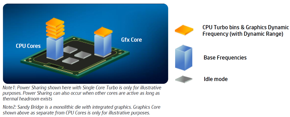
The i7-980X held its own against the new mid-range CPU in our gaming tests, managing to crank out an extra 1fps from Crysis when both CPUs were at stock speed. However, the much cheaper i5-2500K ran X3: Terran Conflict 8-11fps faster than the i7-980X, which was previously the fastest CPU for this game before the new range was launched.
You’ll notice that we haven’t compared the i5-2500K with anything but the fastest CPUs that Intel and AMD have previously released – it walks all over everything else, as you can see from the performance graphs.
In the power consumption stakes, the i5-2500K proved to be highly energy-efficient, with the PC drawing only 76W from the wall when idle and 148W under load. Those figures compare favourably to cheap, low-end hardware; naturally, the X6 1100T and i7-980X draw more power from the wall by an exponential amount. The power to performance efficiency of the i5-2500K is staggering.
We overclocked the i5-2500K by first setting the Load-Line Calibration of the Asus P8P67 to Extreme. We then set the Base Clock to 104.7MHz and the CPU multiplier to 47x for an overall frequency of 4.92GHz. To make this stable, we set the CPU voltage to 1.35V, the CPU PLL to 1.9V, the VCCSA to 1.1V and the VCCIO to 1.106V. See How to Overclock an LGA1155 CPU for more details on how we overclocked all the CPUs.
The boost from a nominal 3.3GHz to 4.9GHz resulted in phenomenal performance: the overall Media Benchmarks score jumped from 1,889 to 2,687, making the Sandy Bridge system slightly faster than an X58-based PC with a 4.4GHz i7-980X at its heart. We saw incredible performance gains in every application, with the i7-980X only making a case for itself in Cinebench where its six Hyper-Threaded cores overclocked to 4.4GHz managed a score of 11.22.
Conclusion
The Sandy Bridge lineup gives us some of the easiest conclusions to write that we’ve ever come across: the new range of Intel CPUs renders almost every other processor redundant and pointless.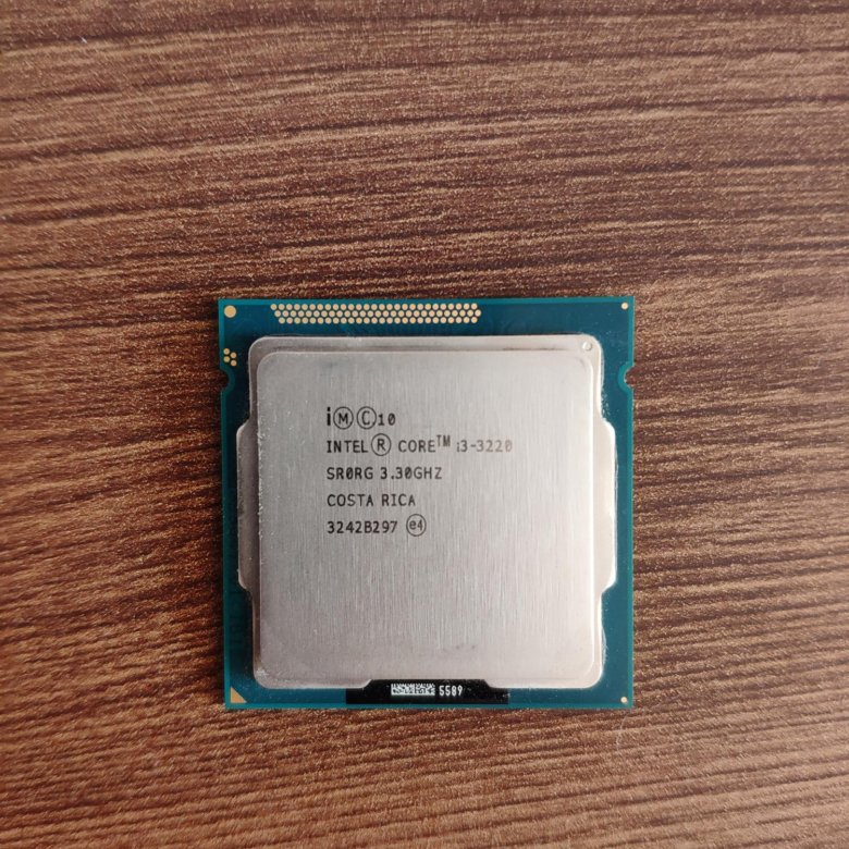 Only if you need incredible performance in multi-threaded applications should you look beyond the Core i5-2500K for your next CPU.
- Performance
- x
- x
- x
- x
- x
- x
- x
- x
- x
- —
- 9/10
- Features
- x
- x
- x
- x
- x
- x
- x
- x
- x
- —
- 9/10
- Value
- x
- x
- x
- x
- x
- x
- x
- x
- x
- x
- 10/10
- Overall
- x
- x
- x
- x
- x
- x
- x
- x
- x
- —
- 9/10
Score Guide
Intel Core i5-2500K
Specifications
- Frequency: 3.3GHz
- Core: Sandy Bridge
- Manufacturing process: 32nm
- Number of cores: 4 x physical
- Cache: L1: 64KB + 64KB (each core), L2: 512 KB (each core), L3: 6MB (shared)
- Memory controller: Dual-channel DDR3, 1,333MHz
- GPU: HD 3000
- Packaging: LGA1155
- Thermal Design Power (TDP): 95W
- Features: SSE, SSE2, SSE3, SSSE3, SSE4, SSE4.
 2, EM64T, EIST, Execute Disable Bit, VT, AES-NI, Turbo Boost 2.0, AVX, Quick Sync Video
1 — Intel Sandy Bridge Review2 — What’s New in Intel’s Sandy Bridge3 — More of What’s New in Intel’s Sandy Bridge4 — Intel Processor Graphics Overview5 — How to Overclock an LGA1155 CPU6 — Sandy Bridge Test Setup7 — Sandy Bridge Cinebench and WPrime Performance8 — Sandy Bridge Image Editing and Video Encoding Performance9 — Sandy Bridge Multi-tasking and Overall Performance10 — Sandy Bridge Gaming Performance11 — Sandy Bridge Power Consumption12 — Intel Core i5-2500K Review13 — Intel Core i7-2600K Review14 — Intel Core i5-2400 Review
Intel Sandy Bridge Review | bit-tech.net
Written by
bit-tech Staff
January 3, 2011 | 04:58
Tags: #comparative #core-i3 #core-i5 #core-i7 #cpu #h67 #k-series #lga1155 #overclocking #p67 #performance #processor #processor-graphics #recommended #sandy-bridge
Companies: #amd #bit-tech #intel
1 — Intel Sandy Bridge Review2 — What’s New in Intel’s Sandy Bridge3 — More of What’s New in Intel’s Sandy Bridge4 — Intel Processor Graphics Overview5 — How to Overclock an LGA1155 CPU6 — Sandy Bridge Test Setup7 — Sandy Bridge Cinebench and WPrime Performance8 — Sandy Bridge Image Editing and Video Encoding Performance9 — Sandy Bridge Multi-tasking and Overall Performance10 — Sandy Bridge Gaming Performance11 — Sandy Bridge Power Consumption12 — Intel Core i5-2500K Review13 — Intel Core i7-2600K Review14 — Intel Core i5-2400 Review
Intel Sandy Bridge Review
Manufacturer:Intel
UK price (as reviewed): TBC
US price (as reviewed): From $117 to $317 (ex tax)
It seems that we’ve been hearing about Intel’s next-gen CPU architecture, codenamed Sandy Bridge, for the past year, and previewing motherboards and revelling in the leaks for at least four months. In fact, it reached the point where we’d said ‘Sandy Bridge’ so often in the office that it started sounded stupid – Intel’s coming in to show us its Sandy Bridge? Wouldn’t a medical professional be more appropriate, we’d joke.
However, that all ended soon after we received our first CPU samples in November and started our own testing. Our conclusions? The Sandy Bridge CPU range is incredible, and has the potential to change the entire PC industry.
Intel’s new CPU has the price and performance to change the PC industry
Intel hasn’t helped at all to convey the significance of its new line-up – the range is still branded Core i3, i5 and i7, making it hard to know whether it’s new at all. The Internet has also been awash with rumours that Sandy Bridge won’t overclock at all, or that it’s so easy to do so and the CPUs are so fast that Sandy Bridge will make the LGA1366 Core i7 range redundant – not bad for a mid-range, mid-priced CPU.
There’s a lot to explain when it comes to the new Sandy Bridge range, so we’ll endeavour to blow away the myths and deliver the facts as clearly and concisely as possible.
How to Spot a Sandy Bridge CPU
Intel is calling Sandy Bridge its second-generation Core architecture, which is wrong. The first Core-branded CPU was a laptop-only CPU based on the Yonah architecture of early 2006, followed by Conroe and its mobile equivalent Merom, which was sold under the Core 2 brand. Ignoring the Conroe update that was Allendale, manufacturing process shrinks of Wolfdale and Penryn, and the Core 2 Quad CPU designs, Intel should have realised that Nehalem counts as a new architecture.
We therefore reckon that Sandy Bridge is Intel’s fourth genuinely new Core architecture, not its second. It’s scandalous that Intel should throw away the excellent pedigree of the Core brand by not recognising this.
The lower line shows the new logo for the Sandy Bridge range – the brand is cracking apart to reveal the underlying technology, rather than peeling off as before. As Intel is erroneously calling all its Sandy Bridge CPUs its second generation of Core CPUs, every model name starts with the number ‘2’. You can also recognise a Sandy Bridge CPU by the four numerals in its model number rather than three, and any CPU with a ‘K’ at the end of its model number as a practically unlocked multiplier (it caps out at 57x, which is plenty for almost every possible use).
1 — Intel Sandy Bridge Review2 — What’s New in Intel’s Sandy Bridge3 — More of What’s New in Intel’s Sandy Bridge4 — Intel Processor Graphics Overview5 — How to Overclock an LGA1155 CPU6 — Sandy Bridge Test Setup7 — Sandy Bridge Cinebench and WPrime Performance8 — Sandy Bridge Image Editing and Video Encoding Performance9 — Sandy Bridge Multi-tasking and Overall Performance10 — Sandy Bridge Gaming Performance11 — Sandy Bridge Power Consumption12 — Intel Core i5-2500K Review13 — Intel Core i7-2600K Review14 — Intel Core i5-2400 Review
What do we need to build a bridge.
 ..
..
Intel has announced its readiness to release in early 2011 processors of the new Sandy Bridge architecture («sand bridge»), which will replace the current Nehalem (45 nm) and Westmere (32 nm). In accordance with the “tick-tock” release rule, Sandy Bridge is “tuck” — a new microarchitecture released on an already established process technology (32 nm). However, at the end of 2011, another tick is expected — a slightly updated 22-nanometer version of Sandy Bridge called Ivy Bridge (ivy bridge). Well, now, while dealing with the sandy brainchild, as an experiment, we will try a new approach — we will use original illustrations from Intel presentations (of course, not all and not entirely), but we will comment on them in our own way 🙂
So we’re being offered processors built (hold on tight!) around «energy efficiency» and «mind-blowing performance» — the best way to make the reader fall asleep from boredom in this very place. However, here is a short list of real advantages compared to the current generation of Intel CPUs:
- The Northbridge of the chipset is now integrated into the chip along with the video core.
- The graphics core (GPU) itself has been updated, but the ability to connect external graphics has been retained.
- General purpose kernels support the AVX extension.
- L3 cache increased throughput due to high-speed connection to cores (including GPU).
- TurboBoost technology has been improved.
Let’s go through these and smaller points.
The coarse-grained CPU core has not changed. It’s all about the details.
In the front, the main innovation is a cache for 1536 uops, which buffers the results of the decoders. The branch predictor has also been redesigned, now storing twice as many target addresses and a longer history of command behavior. It is connected to a block that determines hits in the mop cache, and in these cases, the L1I cache, length predecoder and decoders are disabled, saving power. Performance is also improved by improving the response to a mispredicted branch (the correct branch may end up in the mop cache) and by eliminating the need to decode long instructions for several cycles each time they are executed.
The rear of the conveyor has changed more. First explicit change: moving from a full ROB buffer (storing the uops and the values of the registers they change) to a combination of a shortened ROB (storing only the uops in the original order) and two physical register files (PRFs, storing the contents of the renamed registers that the uops refer to) — an integer and vector-real. The meaning of the transition is that instead of transferring uops, only register references are sent along with the data, and the uops and data themselves remain in place until retirement — as a result of removing unnecessary transfers, energy is saved. And the quite duty increase in the size of the whole variety of buffers and queues is responsible for the performance.
At the functional unit level, the big news is support for AVX, a new addition to the x86-64 instruction set. Unlike the next SSE, which simply adds new commands, AVX allows you to:
- access 256-bit vector ymm registers that extend the usual xmm for SSE;
- use 3-4 operands in non-destructive form in all vector commands, when the result of the operation does not destroy the original arguments;
- save on the size of vector instructions due to code compaction (especially for SSSE3 and beyond).

Of course, there are new instructions for allocating elements in a vector and masked memory operations.
To prevent good intentions from remaining only at the AVX command recognition level, the FU block has been redesigned to process ymm registers at the same speed as xmm. To do this, the 128-bit adder, multiplier, ALU, and shufflers doubled the bit depth, raising the core’s peak performance accordingly.
L1D cache increased total throughput by 50% to 32 read bytes + 16 write bytes per clock. To do this, a second 16-byte read port is installed in the LSU (L1D controller). This will allow you to saturate the FU with data at the right pace when executing the AVX code.
Other kernel updates that didn’t make it onto the charts include speeding up several commands that are important for encryption tasks, as well as saving processor state when switching task contexts in the OS.
In the extra-core (this is how Intel calls the rest of the CPU that is not included in the general-purpose cores), the list of changes opens with a seemingly new (appeared in March 2010 in 8-core Nehalem-EX server chips) 32-byte ring bus , connecting the L3 cache, computing and graphics cores and the «system agent» (the former northbridge with ICP for DDR3 memory). L3, designated LLC (last level cache), consists of several banks (according to the number of general purpose cores) with an access port in each. The ring bus connecting all this operates at a frequency comparable to the frequency of the cores, and ideally transfers an amount of data per clock equal to the product of 32 times the number of banks. In this way, the performance of a shared L3 increases in proportion to the number of cores, but the promised reduction in latency (at least in cycles) is doubtful compared to a centralized L3 controller.
Since the GPU is now located on the processor chip, and not on a separate one, as in the current Core i3 / i5, the L3 cache can also be used for graphics, which alleviates the lack of system memory bandwidth compared to specialized video memory, rarely available for an embedded GPU.
The video core is promised double performance, and not only due to the fast L3 cache, but also from doubling the number of execution units to 12 — though not in all models, which is silent on the diagrams. Also introduced is support for DirectX 10 (and it’s already the 11th in the yard …) and new HD video formats for energy-efficient hardware acceleration of (de)coding.
The CPU will receive triple power — for general purpose cores and L3, for the GPU, as well as for the system agent with various bus controllers. It is not yet clear whether all lines have auto-tuning for the current load, because on the above slide the voltage of the system agent is indicated as fixed, and in the text to another it is written that all voltages can be adjusted.
The thermal and power controller implements an updated version of TurboBoost technology that takes into account transients. It will allow within a short time (20–60 s) to overclock the cores (including the GPU) to frequencies at which the heat dissipation is even higher than the nominal peak (TDP), if the CPU has been idle for some time before. This will provide more responsiveness to short execution time, but computationally intensive tasks.
Processors will ship with a wide range of TDPs and frequencies in different (non-modern compatible) cases for new motherboards. For desktops, this is LGA1155 (2.3-3.4 GHz), and for mobile PCs, PGA and BGA2 (2.2-2.7 GHz). The 60-series chipsets (which, like their predecessors, are only a southbridge) will support SATA-III (at a speed doubled to 6 Gb / s), but there will not yet be USB 3.0. There will also be no system clock generator that has migrated to the south bridge — this means that significant overclocking through the base frequency, fixed at 100 MHz, is possible only with an external generator, which will not be on cheap boards. However, Intel leaves the possibility of overclocking due to the multiplier, which will be unlocked in models with the letter K and can reach a value of 57. Speaking of models, their names will remain in the form of Core i3/i5/i7, but the model number is now 4-digit. In addition to the letter K, it can be supplemented by S (low TDP), T (even more economical) or M (mobile). A little later, server and budget options will be released.
What is the result? Intel has seriously updated Nehalem — without revolutionary breakthroughs, but simply by consistently updating the details of the microarchitecture and introducing all the innovations of the last two years. As a result, we should once again get even faster processors, but remaining within the same thermal limits. Using AVX optimizations, Sandy Bridge promises to run almost twice as fast as Nehalem, but even without that, the rest of the innovations will not make you bored while waiting. Which, of course, we will check.
For those who are interested, the picture will turn out to be much more interesting if you examine the «sand bridge» in detail, compare it with its main competitor — AMD Bulldozer processors coming out 8-10 months later — and find a lot of both unexpected coincidences and cardinal differences. Wait for our new reviews!
October 8, 2010
Tasit Murki
News0003
February 10, 2023
Is this really an enthusiast processor? Xeon W7-2495X loses to Core i9-13900K in Geekbench test
February 10, 2023
One of the most unusual motherboards. Asus X670 Mini-ITX has one of the chipset chips located on a hidden separate board
February 9, 2023
Newsroom >
Intel Core i5 and Core i7 processors with Lynnfield 9 core0001
( Socket
LGA1156 ).
Platform
Intel
LGA1156
came out officially. Although processors
Lynnfield
and the P55 chipset were introduced by Intel
September 6, 2009, buy older model
processor core
i7-870
could have been at the end of August. Consider
overview of two Lynnfield processors:
Core
i5-750
and Core
i7-870,
for the new platform
LGA1156.
For
start some theory. Processors
Lynnfield
are derived from Bloomfield,
i.e. Core processors
i7
nine hundredth series, intended for
connector LGA1366. Both options are based on
based on the Nehalem architecture
and the differences between them are not so great.
Small simplifications allowed Intel
create a platform that in the future
designed to replace the Core architecture
2 in the mass market, although now the cost
new processors are far from mainstream.
Simplification
Nehalem architecture
in new products affected mainly
only a memory controller that lost
one of the three channels and became familiar
two-channel. In addition, Intel
moved the PCI controller
Express
2.0 into the processor, which made it possible to reduce the cost
chipset for it because it’s expensive
QPI interface
(Quick
Path
interconnect)
for connecting the processor and the northbridge
chipset is no longer required, as,
in fact, the north bridge itself.
|
|
|
Diagram of the structure of the nucleus |
New
P55 chipset supporting processors
LGA1156, consists of only one chip
– the south bridge, which is connected with
processor via bus DMI
( Direct
Media
Interface —
with peak throughput 2
Gb/s Is it a lot or a little? So to speak —
enough. After all, the main data exchange
happens between the processor, video card
and RAM, and controllers
the last two are in the very
processor: Intel engineers
maintained communication via QPI between
cores and a PCI-E controller in the
processor. 2 Gb/s DMI bus is enough
for data transmission over the network, exchange with
hard drives or USB bus, so
special loss of performance of new
products compared to Bloomfield be no
must.
However
PCI controller
Express
in Lynnfield processors
has a total of 16 separable lines, while
time as Intel chipset
X58
can provide up to 36 PCI lanes
Express
through the northbridge. So
way, based on Intel P55 and processor
LGA1156 can build SLI/CrossFire system
in PCI-E x8+x8 mode. Although some maternal
boards are equipped with three PCI-E x16 slots, but
they work in x8 + x8 + x4 mode — additional
four PCI lanes
Express
provided by the chipset (southern
bridge) P55. It is obvious that in this case
the communication bus between the processor and the DMI chipset will be
overloaded, which will affect the efficiency
3-Way SLI mode. However, hardly economical
the user will build the system with
multiple GPUs
on an economical platform, which is planned
make LGA1156: maximum can be set
two video cards without much loss of them
efficiency.
Characteristics
Intel processors
Core
i7-870
and Core
i5-750
differ insignificantly from each other. Apart from
different frequencies, the main difference
is the lack of Core processors
i5
Hyper technology support
threading.
|
Table 1. |
|||||
|
Options |
Core i7-870 |
Core i7-860 |
Core i7-860s |
Core i5-750 |
Core i5-750s |
|
Clock |
2. |
2.80 |
2, 5 3 |
2.66 |
2, 4 0 |
|
L3 |
8.0 |
8.0 |
8.0 |
8.0 |
8.0 |
|
Number of cores/threads |
4/8 |
4/8 |
4/8 |
4/4 |
4/4 |
|
Hyper Trading |
+ |
+ |
+ |
– |
– |
|
Availability |
Core i7 |
Core i7 |
Q1 2010 |
Core i5 |
Q1 2010 |
 93
93
Corporation
Intel began shipping the Core i5-750 chip together
with two other quads
Core i7-860 and Core i7-870 in the early days of autumn
2009d. These chips operate at frequencies of 2.66
GHz, 2.8 GHz and 2.93 GHz respectively, and their
TDP is 95 watts. Except
Moreover, in early 2010 this list will be
replenished with two energy efficient
Core i5-750s and Core i7-860s models with clocked
frequencies of 2.4 GHz and 2.53 GHz and an indicator
TDP at 82 watts.
These
Core i5 processors have the same L3
Cache
(8 MB) as well as technology support
virtualization of VT-x and socket LGA 1156, which
Core i7 chips. However, they lack
support for VT-d function as well as technology
Hyper
threading,
to bring the number up to eight
processed CPU computing
streams.
At
this auto overclocking function
Turbo
boost,
also present in all new
processors, allows you to increase the frequency
one of the cores of Core i5-750, Core
i7-860 and Core i7-870 up to 3.2GHz, 3.46GHz and 3.46GHz
respectively.
Externally
new processors less processors
bloomfield,
which is quite natural. Quantity
contacts decreased — in fact,
their number is placed in the name of the sockets
Intel
— because the dimensions of the processors have changed.
Physically, the processor is made in one
core, however Lynnfield
with a core area of 296 sq. mm. contains 771
million transistors, while
Bloomfield
(Core i7-9xx) — 731 million with a core area of 263
sq. mm. The appearance in new
PCI controller models
express.
Not
forget to mention the new version of the technology
Intel Dynamic Overclocking
Turbo
boost,
introduced with Core i7-8×0 and Core
i5-750. Turbo
Boost
was implemented back in Bloomfield
and allowed to increase the multiplier beyond
standard (for example, x20) per unit,
if three or four cores worked; or
by two if one core worked. In new
Turbo processors
Boost
became more aggressive: Core i7-8×0 increase
multiplier by two steps in the case
activity of 3-4 cores, and Core i5 only on
one step; but in the case of two active
cores all Lynnfield processors
can accelerate by 4 steps, and in the case of
with one stream — five steps (667
MHz!).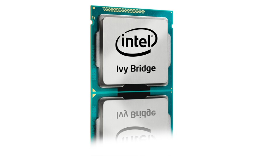 What will it give in practice? It is known
that multithreaded programs win
in performance when using
more cores, but single-threaded
applications are more frequency sensitive
kernels. In this case Lynnfield
performs very well, especially
in games that do not use multithreading.
In practice, during testing, we
managed to see an increase in the multiplier
four steps, which is not bad
result: as you may know,
to increase the multiplier to two
steps from Bloomfield
was problematic.
So
way, together with inexpensive
chipset, new Intel processors have
every chance to become popular in the segment
mainstream.
If the Core i7-9xx plus motherboard is on
based on the X58 have a fairly serious
cost, the new platform will not
for example more economical, especially with
Core i5 processor.
Differences
in memory subsystem performance
between Core i7-870 and Core i5-750 are small, however
in single-channel mode, the Core i7 noticeably
faster, but much more different
latency — i7 ahead. A loss
performance compared to
three-channel mode, of course,
there is, but it is not as critical as it could
appear earlier: yet built-in
processor memory controller its role
plays, it is enough to compare with
memory subsystem performance
platform LGA775, for which the values
more than 10 Gb / s are simply unattainable in
most cases. Therefore, to work
with databases in inexpensive office
servers new processors are fine
fit.
Without
Hyper
threading
processors show close
performance.
Corporation
Intel plans to move from
already existing 32 nm process technology on
thinner 22nm technology. This
the transition must take place in the fourth
quarter of 2011. So Intel
trying to stick to his plan
and submit a new one every two years
kernel type.
Further
in the corporation’s official roadmap, we
we see the following of the same tradition. IN
fourth quarter of 2013, Intel plans to
switch to 15 nm process technology, and even later
two years the global chipmaker must
present workable 11 nm
solutions. Finally, in a very remote
in the future, it is planned to release the CPU,
whose dimensions will be 80 percent smaller,
than 11 nm chips. Perhaps he will
be created according to the standards of 7 nm technology.
Data
plans look quite intriguing,
but quite feasible, if, of course,
Intel will not face purely technological
problems. So far, it is not entirely clear
on what principles can
such «thin» processors. At the same
time Intel competitor GlobalFoundries
two years behind the given
graphics, at least with mastering
32 nm and 22 nm process standards. However, when
sufficient capital investment
can even outpace the current
industry leader.
Confusion with
names
Although
product range seems simple
and unambiguous — Core i3, Core i5 and Core i7 — Intel all
left a few «underwater
stones» to remember.
Processors
Core
i 3
are dual-core CPUs. They don’t have all those
features that are present in more
expensive models. These are the processors of the initial
level, while the market has
only two models — i3-530 at 2.93 GHz and i3–
540 at 3.06 GHz.
Processors
Core
i 5
available
as with two cores (model number
600) and with
four cores (model number 700) .
All processors support technology
Turbo Boost, but only two models
hardware accelerated AES encryption and
offer Hyper-Threading support.
Quad core processor
i5-750
manufactured in 45nm process technology
dual-core models — according to the 32-nm process technology.
Finally,
exists and ruler
Core
i 7 .
The 800 series runs on the same socket as
and the processors mentioned above, namely
Socket
LGA
1156. These processors support
hyper-threading,
but don’t have hardware acceleration
AES encryption. high-end
core model
i7-980X
equipped with six cores, produced
based on 32nm process technology and has acceleration
AES, and the rest of the processors in the 900 line
have only four cores (no AES).