What Is MOSFET? A Basic Definition — Tom’s Hardware
Skip to main content
When you purchase through links on our site, we may earn an affiliate commission. Here’s how it works.
A motherboard with MOSFETs circled in yellow. ( (Image credit: Shutterstock))
MOSFET stands for metal oxide semiconductor field effect transistor. In the PC world, you’ll find these electrical components on a desktop or laptop motherboard , as well as a desktop power supply unit (PSU) .
Motherboard MOSFETs
On a PC, MOSFETs help make up the VRM (voltage regulator module), which controls how much voltage other components on the motherboard, like the CPU or graphics card , receive.
PC components like CPUs and graphics cards have strict operating voltages, so a motherboard’s VRM helps make sure this isn’t exceeded. MOSFETs are important to VRM functionality and have an impact on the amount of heat being generated by a VRM while it’s doing its job. MOSFETs can get quite toasty if you’re using a powerful graphics card , and a motherboard’s heatsink helps cool the MOSFETs and, thus, the VRM. In addition to keeping the overall system safe, keeping MOSFETs cool is also important for any type of overclocking .
How Do They Work?
MOSFETs are like switches that go on and off based on a signal from an integrated circuit (IC) called the PWM chip / controller. MOSFETs switch on and off quickly, allowing high current to flow through in short bursts. This, along with other parts of the VRM, controls voltage sent to other PC components on the motherboard.
To keep motherboard MOSFETs cool during extreme overclocking, PC enthusiasts often use waterblocks. Vendor EK also makes Monoblocks, which is a shared CPU and MOSFET waterblock.
MOSFETs and Power Supplies
MOSFETs perform a similar function on PC power supplies.They’re used in convertors and regulator circuits for switching purposes in switched-mode power supplies (SMPS).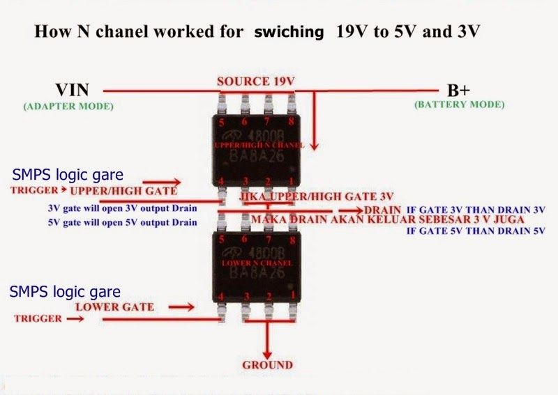
In an SMPS, energy is pulled from an AC socket before its broken down into small packets with the MOSFETs acting as switchers. Those packets are then carried via capacitors , inductors and more electric components capable of storing energy. Ultimately, the packets merge into one for a single, and steady, output.
This article is part of the Tom’s Hardware Glossary .
Further reading:
- Dissecting the Modern Motherboard: Connectors, Ports & Chipsets Explained
- Best Motherboards
- Best Power Supplies
Get instant access to breaking news, in-depth reviews and helpful tips.
Contact me with news and offers from other Future brandsReceive email from us on behalf of our trusted partners or sponsors
Scharon Harding has a special affinity for gaming peripherals (especially monitors), laptops and virtual reality. Previously, she covered business technology, including hardware, software, cyber security, cloud and other IT happenings, at Channelnomics, with bylines at CRN UK.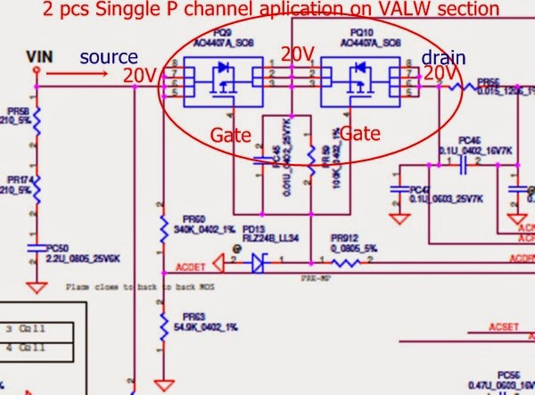
Tom’s Hardware is part of Future US Inc, an international media group and leading digital publisher. Visit our corporate site .
©
Future US, Inc. Full 7th Floor, 130 West 42nd Street,
New York,
NY 10036.
Mosfet Type on Laptop Motherboard
There are 4 type of mosfet’s SO8 on laptop motherboard
1. P channel mosfet
2.N chanel mosfet
3.dual P channel mosfet
4.Dual N chanel mosfet
each type could substitute as long as same type even with different marking code.
Easy way to identified look at the end number of marking code .
example :
AO 4433 look at end of marking code number is odd numbers ( 3 )
this is P channel
example : AO 4407 (7) is odd number ,this is P channel too,
they could be substitute each other even different manufacture and code.
Others P chanel examples :
AF 4825-AM 3423-FDS 6679-SI 4835 ETC
Other example : AOD 4466
look
at last number of marking code it is even (6) numbers it’s mean this is
N channel mosfet and they could replace by other N channel even
different
manufacture and code .
Others N channel mosfet examples: AO 4800
AO 4474-AP 4232-FDMC8844-SI 4812 ETC
those mosfet identified only for SO8 mosfet.
We can see P channel mosfet function on this «GENERAL LAPTOP MAIN POWER « layout link :
https://www.facebook.com/photo.php?fbid=558040790910547&set=o.1403489539873697&type=3&theater
There are only 3 pcs P channel there ,2 pcs ADP(adapter) fet’s and 1pcs Bat (battery)fet .some
motherboard also may have 1 adp Fet,some replace with diodes to supply every adapter supply need.
I
call it «VALW MAIN LINE» .from this line Battery ic and dc/dc power
supply ic get VCC to powered each ic and this main VALW line also
distributed adapterVoltage to every N channel Source ,before they got
enable trigger to produced 3 and 5V_ALW……
P-channel mosfet works drain is a input for nagative supply and source is a output for nagative supply ,and it’s gate on with nagative volt . same way if you want to drive positive supply from p-channel mosfet then souce is input and drain is output for positive supply .
This is How 2 pcs P chanel replace by 1 Dual P chanel Mosfet
Look
at this lay out function N channel mosfet as integrated circuit with
DC/DC main power supply to produce 3V and 5V_ALW in this link :
https://www.facebook.com/photo.php?fbid=559969450717681&set=o.1403489539873697&type=3&theater
and
what happen if P or N channel leak and what if suppose N channel
replace with and P channel and what damage it could be on this link:
https://www.facebook.com/photo.php?fbid=566258196755473&set=o.1403489539873697&type=3&theater
How
DC/DC main power supply open/close gate N channel to produce 3V and
5V_ALW and important signal enable/disable function to activate the
DC/DC main supply ic (ISL 6237-RT 8206-TPS 51247) on this link:
https://www.facebook. com/photo.php?fbid=566251166756176&set=o.1403489539873697&type=3&theater
How do (RT8223-TPS 51125-TPS 51123)work and signal need on this link :
https://www.facebook.com/photo.php?fbid=566250426756250&set=o.1403489539873697&type=3&theater
If you confused ,you should read this before
Introduction of System Power Laptop Motherboard in this link
https://www.facebook.com/groups/BoardlevelRepair/doc/1414775788745072/
and to avoid accident before repairing you shoul read
THINGS THAT SHOULD NOT BE TAKEN IN MOTHERBOARD REPAIR
in this link :
https://www.facebook.com/groups/BoardlevelRepair/doc/1414337728788878/
We will also found (SO3) P channel ,(SO8) mean mosfet have 8pin and (SO)3 mean they
have 3 pin.And this (SO3) also have P or N channel type .so be ware if you
want to make replacement .just make sure replace it whit same type .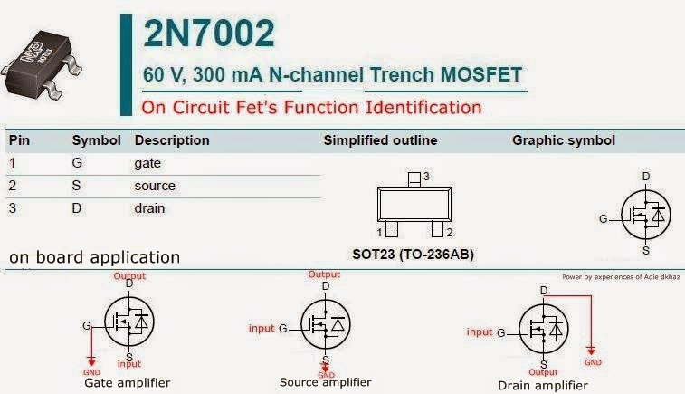
Other way to Identified for (SO6) and (SO3) Mosfet transistors are by finding the marking code on ic than
browse the data sheet , if they not found get mosfet location code on board than
find
on schema by typing marking code to adobe reader search column to look
the correct marking code than browsing the datasheet again to get know
mosfet type and get substitution…
this is one of sample N channel (SO3) code : 2N7002 -P0603BDG
samples (SO3) P channel mosfet :
FDD6685 — SI12301 -TP0610K.
sample datasheet link for N channel (SO3) 2N7002 : http://www.fairchildsemi.com/ds/2N/2N7000.pdf
2 mosfet in one package ,it is a simply vrm switching mosfet circuit in single mosfet package ,drain connected with diode cathode and source is connected with anode that how to identified a N-Channel mosfet.
N chanel caracter common base
n-channel mosfet voltage flow is drain to source for positive supply — when you apply + positive volt in gate then this mosfet drive voltage drain to souce ( gate works same as transister base) if you want to drive nagative volt from n-channel mosfet then nagative volt drive source to drain mean for nagative volt input is source and output is drain
n channel mosfet logic low (vi) that mean mosfet not close circuit between the drain and source ,v_out you got vdd voltage via resistance .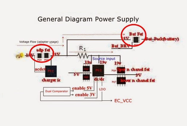 (Hi)
(Hi)
when you apply vi = Hi in N-Channel mosfet ,mean drain to source connected (close circuit) in this case you got v_out source low you can got at v_out .same way in P-channel but gate work reverse as n-channel mosfet work
Additional board to strengthen regular mosfettes on Flying Bear Ghost 5
Technician
additional boards with mosfets of higher power and connect the heaters of hot ends and tables in it.
In addition to the options offered by Chinese manufacturers, for example: https://aliexpress.ru/store/group/Heatbed/1047297_517227812.html, is also developed in the Russian Federation. Sold here http://www.cheap3d.ru/shop/Zapchasti-dlya-printerov/Plata-kommutaoeii-Cheap3D-MOSFET-Switch-Board-55A-v20—1403.html
When buying, pay attention to execution options. In my case, I planned to connect to the outputs of regular mosfets, so I took it to 24V.
The description bribed me. The board has an optocoupler. Mosfets require neither heatsinks nor active cooling, as long as the load limit is not exceeded. In the power section, counter protective diodes are installed that protect transistors from breakdown during voltage surges that occur when working with inductive loads. Two channels — one can be connected to the table, the second to the hot end. And the price is great. Add. outputs for connecting something else, small.
I’ve been wondering for a while where to install this board. Techie’s Corner offered a variation https://youtu.be/RegVBCkNDRE?t=803 which inspired me to delve deeper into the printer’s basement and explore the existing holes.
I tried on the proposed mounting option for the Cheap3D board, and realized that it would have to be redone. And I even started, but then I looked at the place where the table plume entered.
At this point, the cable is pressed with a plastic bridge on two screws.
Having measured all this economy, I sketched the model in Fusion360 and printed it from PLA for fitting. The fitting revealed a number of points that I eliminated and printed the final copy from ABS.
In it, I provided a lid pocket that covers the cable entry window to limit dust from entering the basement, as well as the possibility of accidental contact with the terminal block pins on the back of the board.
The design also included gills for passive ventilation and stiffeners.
The holder is installed in a regular place instead of the table cable clamp and fastened with the same screws.
The board is attached to it with 4 M3 screws up to 10mm long. Holder height 11 mm.
It is advisable to use dielectric (not metal) washers so as not to damage the board. Although, at the attachment points, a bypass of the screw fasteners is provided, and the diameter of the bypass reaches 9 mm.
The table cable comes out neatly from under the holder, wraps and connects to the board. Just don’t forget about polarity. It’s easier if you mark the poles of the wiring before unscrewing it from the motherboard. Otherwise, you have to crawl under the table and ring the pins.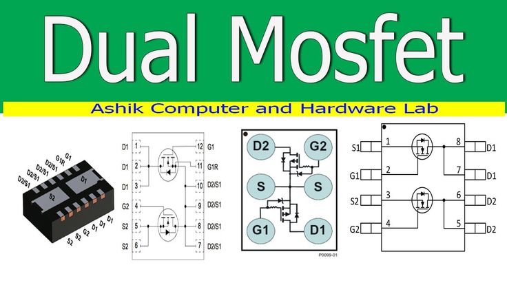
In addition to screws, you will need KF2510 2-pin connectors (female, 2-4 pcs.) And U-shaped terminals (8-10 pcs.), The characteristics of which are well described in the datasheet for the board http://www.cheap3d.ru/ shop/cheap3d_mosfet_switch_board_datasheet_2.0_ru.pdf.
In principle, KF2510 3-pin is also possible, they also hold well, and they can also be torn off from old coolers from a computer. I did not expect that they would come in handy — the «plushkin» rejoiced in me.
Don’t forget the jumpers after installation! Their functions are described in the datasheet. I took them both off.
The terminals are crimped with a crimper; without it, pliers will be very hard and the insulation of the terminals will be damaged. Almost all switching is backwards compatible. The only but is the need to put the terminals on the power wires of the table. Necessity — because without terminals, the contact in the terminal block will not be very good and the connection may heat up. Here is the proof from the Cheap3D datasheet:
After switching, of course, I turned everything on and watched. In the process of heating the table to 100 Chinese degrees, the regular mosfet on the motherboard heated up to 37 degrees. Mosfet on the board up to about 40. But since. the board is located next to the passing air flows from the standard cooler, then these readings only show that the board with a large margin does not heat up at all on the drain.
I recorded a short video about this, where you can see by the LEDs how the PID on the motherboard and on the board works synchronously: https://www.youtube.com/watch?v=imun2tuF3Nw I have a table on channel A, and a hot end on B. So the terminal block is closer to the table cable.
PID calibration has not changed much, you don’t even have to recalibrate — nothing will change for the printer.
Happy as an elephant. Now long presses at high temperatures do not frighten me as a beginner.
This is how the layout turned out.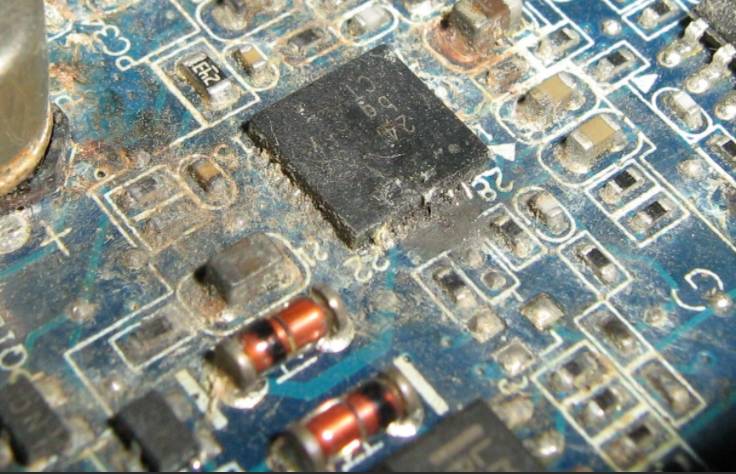 Pretty decent, in my opinion, as Sorkin says.
Modernization with little blood with minimal intervention and backward compatibility, the profit from which is the price of a potentially burnt motherboard (read — extending its service life).
Holder model can be downloaded here https://3dtoday.ru/3d-models/detali-dlya-3d-printerov/raznoe/derzatel-platy-cheap3d-mosfet-switch-board-55a-v20-na-statnoe-mesto -fbg5
If someone is itching to upgrade the model, add the ability to install a cooler above the board.
mosfet
FBG5
MOSFET
Cheap3D
Subscribe author
Subscribe
Don’t want
10
MOSFET | ROM.by
Home
All modern digital technology is built mainly on field MOS (metal-oxide-semiconductor) transistors (MOSFETs), as more economical, compared to BT, elements. Sometimes they are called MIS (metal-dielectric-semiconductor) — transistors. The international term is MOSFET (metal-oxide-semiconductor field effect transistor).
Hello people. tell a beginner: how can I replace the me4932a-g transistor? I have a manual for it. I tried to find a replacement for him, but apart from AO4932 nothing comes to mind. But this one does not fit either: the Vgs of the original is 20 / 20V, the analogue is 12 / 20V. me4932a-g-assembly with asymmetric transistors (1 channel-10.2A, 2-9A). 1st channel with a Schottky diode, 2nd channel with a diode. The system operates at a frequency of 300-350 kHz (up6122aqkf / af PWM). Covered with a shim and strapping.
I apologize right away if I didn’t create the topic correctly. The problem is as follows, There is a WINFAST 6100K8MA-RS motherboard, and everything seems to be working fine in terms of starting and loading Windows, the USB ports are working and working, the sound and video also work. but there is the problem with the heating of the Q32 transistor is very strong heating, it burns, the south bridge heats up about 60 degrees. Alas, there is no circuit.0003
Friends, such a disaster. The second time the motherboard was under repair, the first time the transistor burned out:
Lower arm: APM2558N (25V/60A, Rds=4.5mOHM@V=10V / Rds=7.5mOHM@V=4.5V)
I replaced it with an analog, and The motherboard worked properly for 8 months, and again the same story… moreover, this tranny got warm, not so much, but…
Hello everyone!!!!
There is an ASUS P6T WS PRO motherboard with a problem that does not turn on.
Revealed a short circuit in the power supply of the processor, found a pair of punched transistors.
Replaced tranzyuki when turned on again struck one. On the reverse side of the board there are ADP3110A (L3E) key management drivers. I replaced the drivers opposite the mosfets that were broken.
When turned on, the same mosfet breaks again. I replaced the EPU ASP0800 PWM controller and still breaks through the same mosfet.
Tell me where to dig further?
Health to all!
The topic is this: there is a mammoth, motherboard asus P5B-VM (aka 60-MBB4R5-B01 in the catalog for BoardViewer).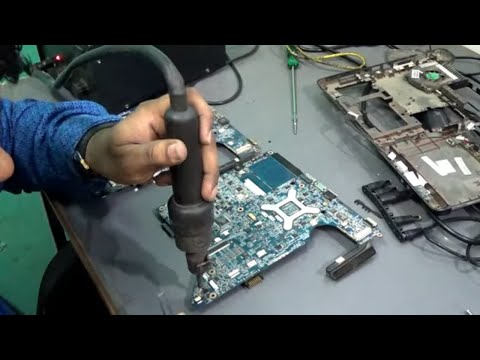 Served faithfully for a long time and works, pah-pah, stably. BUT.
When examining the board, a dimming of the textolite was found in the area of two mosfets (correctly called?) AP60T03GH (PQ34 and PQ36), which, as I understand it, feed the north bridge and memory. The «finger method» reports that they, mosfets, are very hot. Straight at all. I don’t want the board to degrade… The easiest way, probably, would be to unsolder them and stick them on heatsinks?
Hello everyone! In general, there is a Gigabyte GA-H61M-D2H board. Came to me with a kz on nutrition proca. In the second phase, I found a burnt mosfet 4927N, it is designated as (DQ10) on the board. I change it, turn it on and smoke comes out of it. Next, the ISL6609 driver changes with a set, I change the ISL6364 PWM, the phase without mosfets and the driver is called for the presence of a short circuit or dead smd, but everything is fine. Switching on and the same mosfet on the same phase is on again …
Not a working GA-780T-D3L board fell into the hands.