nVidia GeForce GTS 250, just another 9800GTX+? – goldfries
The release of the GTS 250 – a new product to the newbies but to us seasoned users, we’re pretty sure this is just a “rebadge”, so to speak.
Even sites like Anandtech had an article on it, being a smaller-fry in the computer hardware reviewer arena – I can say I’m pretty much left unnoticed by companies like nVidia but that’s not a stopping block for testing out the GTS 250! ?
A Brief Word
*It’s long winded but I just have to get it off my chest. You could skip it to the next section*
From my side of the camp, I’m VERY sick of nVidia’s renaming game! From 8800GS to 9600GSO. Alright, fine……. then we have the 8800GT made into 9800GT, and how 8800GTS was turned into a 9800GTX! I’ve highlighted this on one of my articles before, about more than half a year ago.
nVidia’s silly naming convention, with 9800GTX (a really nice name) given to a card like this just doesn’t make sense.
Like what a friend of mine over at TechARP mentioned – the 9800GTX should be named the 8900 or something, which I whole-heartedly agree. It’s not even a class ahead, let alone a generation ahead
Now let me try my best to illustrate to you HOW BAD is renaming a card from 8800GTS to 9800GTX and yet performing the same. in nVidia’s product line-up, the 1st digit of the 4 digit model name indicates generation. Then the 2nd digit among the 4 indicate the performance level. After that, the alphabets, they represent another finer seperation between performance level. Hence you see, 9600GSO, 9600GT, then 9800GT, 9800GTX, 9800GTX+ and so on.
Understand the naming convention now? Good, if you look at the name alone, the 8800GTS and the 9800GTX are 1 generation apart, and the GTX indicates that it’s another sub-sub-level higher than the GTS (example, 8800GTX was higher than 8800GTS) but performance wise, they’re the same card!
To put it into perspective, if it was coming from ATi then it’s pretty much like saying a HD3850 performs like a HD4870! That’s how bad it is! Fortunately this isn’t the case for ATi, they did a really good and honest job with their naming convention and HD4870 is really far a head of the HD3850.
nVidia is fiendishly clever this time around, moving the name to GTS 250, following the steps of the higher range GTX 260 / 280 GPU – the first generation of GTsomething GPU but it’s still the same thing! Performance-wise that is, arguable one can’t exactly say it’s a rebadge because there are subtle changes but to the eyes of enthusiasts, having the same thing improved does not merit is a whole new name that misleads.
On an interesting note, there’s also news of NVIDIA blacklisting review sites for GTS250 card.
nVidia – I personally think you have great cards but rebranding them is just shameful.
On With The Comparison!
Ok, enough of rants. I hope nVidia stops this nonsense.
In this article, I’ll be comparing the GTS 250 and 9800GTX+ and both are of different brand. ? Both are using same driver version, which is Forceware 182.06. I’ll be updating this article during the weekend with the 182.08 driver to see if there’s any improvement for both cards.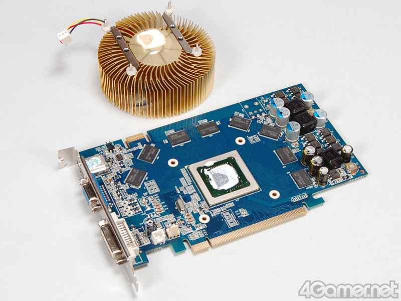
UPDATED : 182.08 driver benchmark results added.
Yeah I know, this could be a GTS 250 vs 9800GTX+ article but I know it’s going to be long winded and all, so I’ve decided to have separate articles for those 2 cards. No, I’m not unveiling them yet…….. ? but the articles will be released within the week.
Test Setup
The computer setup used for this review.
The Contenders
UPDATED : 9800GTX+ card revealed. ? GTS 250 revealed too!
The Palit GTS 250 512MB, as you can see even the latest GPU-Z (v 0.3.2) mis-detected it as a 65nm GPU.
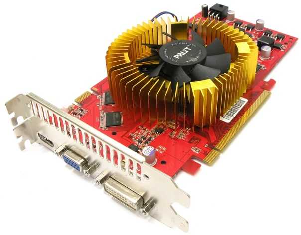
The Forsa 9800GTX+ 512MB
UPDATED : I’ve decided to add the ASUS EAh5850 TOP to the contender list.
The ASUS EAh5850 TOP (I’ll publish an article on this fella in a week or 2)
As you can see, the GTS 250 has a very negligible lead in core and shader speed. Something I couldn’t be bothered to configure to match as the effects of a 7mhz lead is actually too insignificant.
The Performance
All tests were done with 4xAA
F.E.A.R.
Graphic Detail : Maximum at 1680×1050
| Card | Average |
| GTS 250 | 78 |
| 9800GTX+ | 82 |
| GTS 250 (182.08) | 79 |
| 9800GTX+ (182.08) | 82 |
| ASUS EAh5850 TOP | 83 |
World In Conflict
Graphic Detail : Maximum @ 1680×1050
| Card | Average |
| GTS 250 | 27 |
| 9800GTX+ | 29 |
| GTS 250 (182.08) | 28 |
| 9800GTX+ (182.08) | 29 |
| ASUS EAh5850 TOP | 20 |
Company Of Heroes : Opposing Fronts
Graphic Detail : Maximum @ 1680×1050
| Card | Average |
| GTS 250 | 40.6 |
| 9800GTX+ | 41.0 |
| GTS 250 (182.08) | 40.3 |
9800GTX+ (182.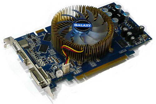 08) 08) |
40.8 |
| ASUS EAh5850 TOP | 48.1 |
Lost Planet : Extreme Condition
Graphic Detail : Maximum at 1680 x 946
| Card | Snow (Average) | Cave (Average) |
| GTS 250 | 43.2 | 56.0 |
| 9800GTX+ | 45.1 | 57.7 |
| GTS 250 (182.08) | 42.3 | 56.5 |
| 9800GTX+ (182.08) | 45.1 | 58.1 |
| ASUS EAh5850 TOP | 49.6 | 59.6 |
Crysis
Graphic Detail : Maximum @ 1680×1050
| Card | Average |
| GTS 250 | 11.08 |
| 9800GTX+ | 12.45 |
| GTS 250 (182.08) | 11.85 |
| 9800GTX+ (182.08) | 10.77 |
| ASUS EAh5850 TOP | 14.11 |
Devil May Cry 4
Graphic Detail : Maximum @ 1680×1050
| Card | Scene 1 | Scene 2 | Scene 3 | Scene 4 |
| GTS 250 | 103. 57 57 |
72.29 | 124.25 | 75.26 |
| 9800GTX+ | 107.69 | 77.09 | 124.77 | 81.37 |
| GTS 250 (182.08) | 104.05 | 71.24 | 123.40 | 76.62 |
| 9800GTX+ (182.08) | 107.86 | 75.35 | 128.76 | 79.34 |
| ASUS EAh5850 TOP | N/A because I didn’t test with it. | |||
Furmark
Graphic Detail : Maximum @ 1680×1050
| Card | Average |
| GTS 250 | 7 |
| 9800GTX+ | 7 |
| GTS 250 (182.08) | 7 |
| 9800GTX+ (182.08) | 7 |
| ASUS EAh5850 TOP | 25 |
I’m pretty much a little surprised that it actually is a little slower despite having slight edge.
Power Consumption
Peak power consumption of idle and load were taken, using Gigabyte Odin GT power supply and the Power Tuner software./data/ET_1600.png)
| Card | Idle | Load |
| GTS 250 | 81w | 148w |
| 9800GTX+ | 89w | 143w |
Looks like the GTS 250 is more effective in power consumption.
Conclusion
So there ya have it. So is it safe to say the GTS 250 is a 9800GTX+ ? Yes, I’m convinced.
The performance was so close, it’s hard even to tell them apart. Thanks nVidia, for releasing the same product for probably the 3rd time. I can’t help but feel like I’m using the 8800GTS G92 for the 4th time now, each time with a different name.
Anyway, do also read up the article at TechARP
goldfries rated this product :
Nvidia’s GeForce GTS 250 graphics card
The history of Nvidia’s G92 graphics processor is a long one, as these things go. The first graphics card based on it was the GeForce 8800 GT, which debuted in October of 2007. The 8800 GT was a stripped-down version of the G92 with a few bits and pieces disabled.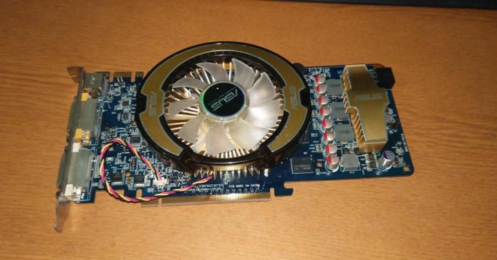 The fuller implementation of G92 came in December ’07 in the form of the GeForce 8800 GTS 512MB. This card initiated the G92’s long history of brand confusion by overlapping with existing 320MB and 640MB versions of the GeForce 8800 GTS, which were based on an entirely different chip, the much larger (and older) G80. Those cards had arrived on the scene way back in November of 2006.
As the winter of ’07 began to fade into spring, Nvidia had a change of heart and suddenly started renaming the later members of the GeForce 8 series as “new” 9-series cards. Thus the GeForce 8800 GTS 512 became the 9800 GTX. And thus things remained for nearly ten weeks.
Then, in response to the introduction of strong new competition, Nvidia shipped a new version of the G92 GPU with the same basic architecture but manufactured on a smaller 55nm fabrication process. This chip found its way to market aboard a slightly revised graphics card dubbed the GeForce 9800 GTX+. The base clock speeds on the GTX+ matched those of some “overclocked in the box” GeForce 9800 GTX cards, and the performance of the two was essentially identical, though the GTX+ did reduce power consumption by a handful of watts. Slowly, the GTX+ began replacing the 9800 GTX in the market, as the buying public scratched its collective head over the significance of that plus symbol.
EVGA’s GeForce GTS 250 Superclocked
Which brings us to today and the introduction of yet another graphics card based on the G92 GPU, the GeForce GTS 250. This is probably the card that, by all rights, the 9800 GTX+ should have been, because it consolidates the gains that switching to a 55nm fab process can bring. Although its base clock speeds remain the same as the 9800 GTX+738MHz for most of the GPU, 1836MHz for the shaders, and 1100MHz (or 2200 MT/s) for the GDDR3 memorythe GeForce GTS 250 is a physically smaller card, at nine inches long rather than 10.5″, and it has but a single six-pin auxiliary power connector onboard.
The reduction in power connectors is made possible by a new board design that cuts power consumption sufficiently to make the second power input superfluous. Although, we should note, Nvidia rates the GTS 250’s max board power at 150W, right at the limits of the PCI Express spec for this power plug configuration.
The GTS 250 is quite a bit shorter than the 9800 GTX
A single power connector will do, thanks
Along with the G92’s umpteenth brand name comes a price cut of sorts: the 512MB version of the GTS 250 will sell for about $130, give or take a penny, well below the price of 9800 GTX+ 512MB cards today. The GTS 250 also offers another possibility in the form of a 1GB variant, which Nvidia and its partners expect to see selling for about $150. That’s quite a nice price in the context of today’s market, where the GTS 250’s most direct competition, the Radeon HD 4850, sells for about $150 in 512MB form. Then again, things change quickly in the world of graphics cards, and Nvidia doesn’t expect GTS 250 cards to be available for purchase until March 10, a whole week from now.
Heck, they may have changed this thing’s name again by then.
There are some benefits to GPU continuity. As you can see in a couple of the pictures above, the GTS 250 retains the dual SLI connectors present on the 9800 GTX, and Nvidia says the GTS 250 will willingly participate in an SLI pairing alongside a GeForce 9800 GTX+ of the same memory size. Unfortunately, though, 512MB and 1GB cards will not match, and Nvidia’s drivers won’t treat a 1GB card as if it were a 512MB card for the sake of multi-GPU cross-compatibility, like AMD’s will.
The card we have in Damage Labs for review is EVGA’s GeForce GTS 250 Superclocked 1GB. Like many GeForce-based graphics cards, this puppy runs at clock speeds higher than Nvidia’s baseline. In this case, we’re looking at a fairly modest boost to a 771MHz core, 1890MHz shaders, and 1123MHz memory. You’ll pay about ten bucks for the additional speed; list price is $159. EVGA also plans to sell a 1GB card with clocks closer to stock speeds for $149. Odds are, neither of those cards will look exactly like the one in the pictures above, which is an early sample. EVGA intends for the final product to have a swanky black PCB and an HDTV out port, which our sample conspicuously lacks.
The Radeon HD 4850 goes to 1GB, too
When we go to review a new graphics card, we tend to look for the closest competition to compare against it. In this case, the most obvious candidate, at least in terms of similar specifications, seemed to be a Radeon HD 4850 card with 1GB of memory onboard. Several board makers now sell 4850 cards with a gig of RAM, and Gigabyte was kind enough to send us an example of theirs.
That handsome cooler is a Zalman VF830, which Zalman bills as a “quiet VGA cooler.” Gigabyte takes advantage of the thermal headroom provided by this dual-slot cooler to squeeze a few more megahertz out of the Radeon HD 4850. The end result is a GPU core clock of 700MHz, up 20MHz from stock, with a bone-stock 993MHz GDDR3 memory clock.
Right now, prevailing prices on this card are running about $189 at online vendors, well above the GeForce GTS 250’s projected price. I wouldn’t be surprised to see AMD and its partners cut prices to match or beat the GTS 250 in the next couple of weeks, but given current going rates, the new GeForce would seem to have a built-in price advantage against the 4850 1GB.
Test notes
You’ll have to forgive us. Since Nvidia sprung this card on us in the middle of last week, and since we rather presumptuously had plans this past weekend, we were not about to go and formulate a revised test suite and produce an all-new set of benchmark results for this card and thirteen or so of its most direct competitors, with all new drivers and new games. Instead, we chose a strategy that very much mirrors Nvidia’s, recycling a past product for a new purpose. In our case, we decided to rely upon our review of the GeForce GTX 285 and 295, published way back on January 15, for most of our test data.
This unflinchingly lame, sad, and altogether too typical exercise in sheer laziness and feckless ridiculosity nets us several wholly insurmountable challenges in our weak attempt at evaluating this new product and its most direct competitor. First and foremost, of course, is the fact that video card drivers have changed one or two entire sub-point-release revisions since our last article. So although we tested the GeForce GTS 250 and Radeon HD 4850 1GB with recent drivers, the remainder of our results come from well-nigh ancient and unquestionably much slower and less capable driver software, because everyone knows that video card performance improves 15-20% with each driver release. Never mind the fact that the data you will see on the following pages will look, on the whole, entirely comparable across driver revisions. That is a sham, a mirage, and our other results are entirely useless even as a point of reference.
As if that outrage weren’t sufficient to get our web site operator’s license revoked, you may be aware that as many as one or two brand-new, triple-A PC game titles have been released since we chose the games in our test suite, and their omission will surely cripple our ability to assess this year-and-a-half-old GPU. This fact is inescapable, and we must be made to suffer for it.
Finally, in a coup de grace fitting of a Tarantino flick, two of the games we used were tested at a screen resolution of 2560×1600, clearly a higher resolution than anyone with a $150 graphics card would ever use for anything. Ever. Do not be swayed by the reasonable-sounding voice in your ear that points out both games were playable at this resolution on this class of hardware. Do not be taken in by the argument that using a very high resolution serves to draw out the differences between 512MB and 1GB graphics cards, and answer not the siren song of the future-proofing appeal. Nothing about this test is in any way “real world,” and no one who considers himself legitimate as a gamer or, nay, a human being should have any part in such a travesty. You may wish to close this tab in your browser now.
Our testing methods
As ever, we did our best to deliver clean benchmark numbers. Tests were run at least three times, and the results were averaged.
Our test systems were configured like so:
| Processor | Core i7-965 Extreme 3.2GHz |
| System bus | QPI 4.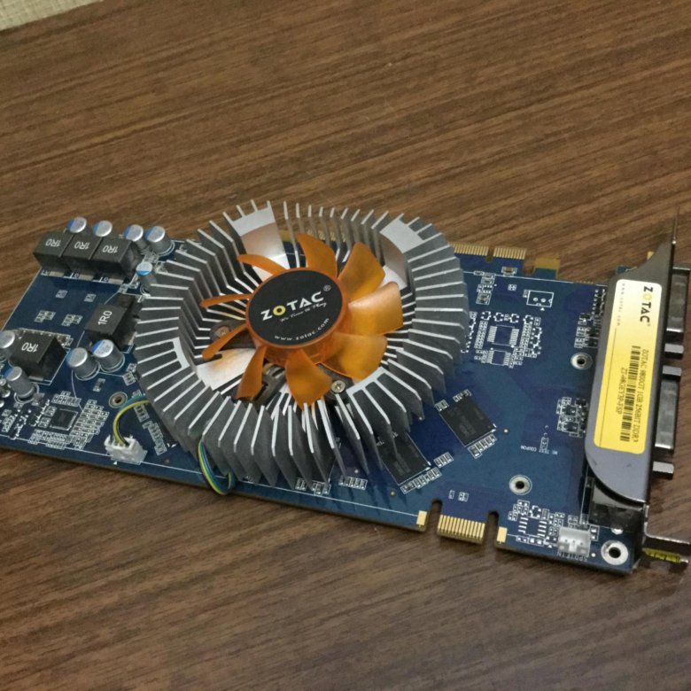 8 GT/s 8 GT/s(2.4GHz) |
| Motherboard | Gigabyte EX58-UD5 |
| BIOS revision | F3 |
| North bridge | X58 IOH |
| South bridge | ICh20R |
| Chipset drivers | INF update 9.1.0.1007 Matrix Storage Manager 8.6.0.1007 |
| Memory size | 6GB (3 DIMMs) |
| Memory type | Corsair Dominator TR3X6G1600C8D DDR3 SDRAM at 1333MHz |
| CAS latency (CL) | 8 |
| RAS to CAS delay (tRCD) | 8 |
| RAS precharge (tRP) | 8 |
| Cycle time (tRAS) | 24 |
| Command rate | 2T |
| Audio | Integrated ICh20R/ALC889A with Realtek 6.  0.1.5745 drivers 0.1.5745 drivers |
| Graphics | |
|
Asus EAh5850 TOP Radeon HD 4850 512MB PCIe
with Catalyst 8.12 (8.561.3-081217a-073402E) drivers |
|
|
Dual Asus EAh5850 TOP Radeon HD 4850 512MB PCIe
with Catalyst 8.12 (8.561.3-081217a-073402E) drivers |
|
|
Gigabyte Radeon HD 4850 1GB PCIe
with Catalyst 9.2 drivers |
|
| Visiontek Radeon HD 4870 512MB PCIe with Catalyst 8.12 (8.561.3-081217a-073402E) drivers |
|
| Dual Visiontek Radeon HD 4870 512MB PCIe with Catalyst 8.12 (8.561.3-081217a-073402E) drivers |
|
| Asus EAh5870 DK 1G Radeon HD 4870 1GB PCIe with Catalyst 8.12 (8.561.3-081217a-073402E) drivers |
|
| Asus EAh5870 DK 1G Radeon HD 4870 1GB PCIe + Radeon HD 4870 1GB PCIe with Catalyst 8. |
|
| Sapphire Radeon HD 4850 X2 2GB PCIe with Catalyst 8.12 (8.561.3-081217a-073402E) drivers |
|
| Palit Revolution R700 Radeon HD 4870 X2 2GB PCIe with Catalyst 8.12 (8.561.3-081217a-073402E) drivers |
|
| GeForce 9800 GTX+ 512MB PCIe with ForceWare 180.84 drivers |
|
|
Dual GeForce 9800 GTX+ 512MB PCIe
with ForceWare 180.84 drivers |
|
|
Palit GeForce 9800 GX2 1GB PCIe with ForceWare 180.84 drivers |
|
|
EVGA GeForce GTS 250 Superclocked 1GB PCIe with ForceWare 182.06 drivers |
|
|
EVGA with ForceWare 180. |
|
|
EVGA + Zotac GeForce GTX 260 (216 SPs) AMP²! Edition 896MB PCIe with ForceWare 180.84 drivers |
|
|
XFX with ForceWare 180.84 drivers |
|
|
GeForce GTX 285 1GB PCIe with ForceWare 181.20 drivers |
|
|
Dual GeForce GTX 285 1GB PCIe with ForceWare 181.20 drivers |
|
|
GeForce GTX with ForceWare 181.20 drivers |
|
| Hard drive | WD Caviar SE16 320GB SATA |
| OS | Windows Vista Ultimate x64 Edition |
| OS updates | Service Pack 1, DirectX November 2008 update |
 12 (8.561.3-081217a-073402E) drivers
 84 drivers
Thanks to Corsair for providing us with memory for our testing. Their quality, service, and support are easily superior to no-name DIMMs.
Our test systems were powered by PC Power & Cooling Silencer 750W power supply units. The Silencer 750W was a runaway Editor’s Choice winner in our epic 11-way power supply roundup, so it seemed like a fitting choice for our test rigs.
Unless otherwise specified, image quality settings for the graphics cards were left at the control panel defaults. Vertical refresh sync (vsync) was disabled for all tests.
We used the following versions of our test applications:
- Call of Duty: World at War 1.1
- Crysis Warhead
- Dead Space
- Fallout 3 1.0.0.15
- Far Cry 2
- Left 4 Dead
- 3DMark Vantage 1.0.1
- FRAPS 2.9.6
The tests and methods we employ are generally publicly available and reproducible. If you have questions about our methods, hit our forums to talk with us about them.
Specs and synthetics
Before we get to play any games, we should stop and look at the specs of the various cards we’re testing. Incidentally, the numbers in the table below are derived from the observed clock speeds of the cards we’re testing, not the manufacturer’s reference clocks or stated specifications.
|
Peak pixel fill rate (Gpixels/s) |
Peak bilinear texel |
Peak bilinear FP16 texel |
Peak memory bandwidth (GB/s) |
Peak shader |
||
| Single-issue | Dual-issue | |||||
|
GeForce 9500 GT |
4. 4 4 |
8.8 | 4.4 | 25.6 | 90 | 134 |
|
GeForce 9600 GT |
11.6 | 23.2 | 11.6 | 62.2 | 237 | 355 |
|
GeForce 9800 GT |
9.6 | 33.6 | 16.8 | 57.6 | 339 | 508 |
| GeForce 9800 GTX+ | 11.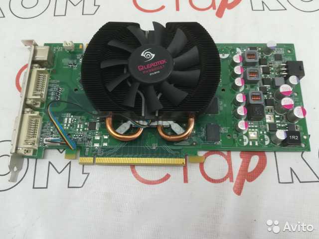 8 8 |
47.2 | 23.6 | 70.4 | 470 | 705 |
| GeForce GTS 250 | 12.3 | 49.3 | 24.6 | 71.9 | 484 | 726 |
| GeForce 9800 GX2 | 19.2 | 76.8 | 38.4 | 128.0 | 768 | 1152 |
| GeForce GTX 260 (192 SPs) | 16. 1 1 |
36.9 | 18.4 | 111.9 | 477 | 715 |
| GeForce GTX 260 (216 SPs) | 17.5 | 45.1 | 22.5 | 117.9 | 583 | 875 |
| GeForce GTX 280 | 19.3 | 48.2 | 24.1 | 141.7 | 622 | 933 |
| GeForce GTX 285 | 21. 4 4 |
53.6 | 26.8 | 166.4 | 744 | 1116 |
| GeForce GTX 295 | 32.3 | 92.2 | 46.1 | 223.9 | 1192 | 1788 |
| Radeon HD 4650 | 4.8 | 19.2 | 9.6 | 16.0 | 384 | – |
| Radeon HD 4670 | 6.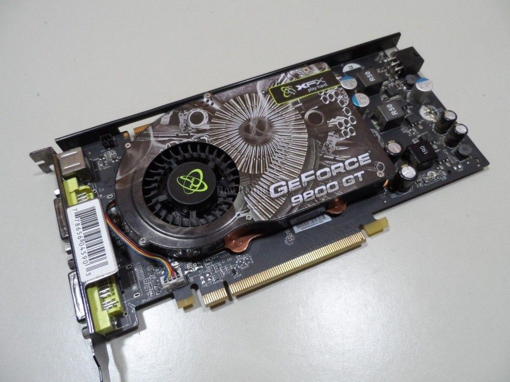 0 0 |
24.0 | 12.0 | 32.0 | 480 | – |
| Radeon HD 4830 | 9.2 | 18.4 | 9.2 | 57.6 | 736 | – |
| Radeon HD 4850 | 10.9 | 27.2 | 13.6 | 67.2 | 1088 | – |
| Radeon HD 4850 1GB | 11. 2 2 |
28.0 | 14.0 | 63.6 | 1120 | – |
| Radeon HD 4870 | 12.0 | 30.0 | 15.0 | 115.2 | 1200 | – |
| Radeon HD 4850 X2 | 20.0 | 50.0 | 25.0 | 127.1 | 2000 | – |
| Radeon HD 4870 X2 | 24. 0 0 |
60.0 | 30.0 | 230.4 | 2400 | – |
The theoretical numbers in the table give the GeForce GTS 250 a clear advantage in texture filtering rates and memory bandwidth, while the Radeon HD 4850 has an equally sizeable lead in peak shader arithmetic capacity. But look what happens when we run these cards through 3DMark’s synthetic tests.
The 4850 1GB nearly matches the GTS 250 in the color fill test, which tends to be bound primarily by memory bandwidth, and the 4850 comes out on top in the texture fill rate test.
Meanwhile, the GeForce GTS 250 leads the 4850 in half of the shader processing tests, and our expectations are almost fully confounded. In this GPU generation, the theoretical peak capacities of the GPUs take a back seat to the realities of architectural efficiency. Although the G92 has more texture filtering potential and memory bandwidth on paper, the HD 4850 is stronger in practice. And although the 4850’s RV770 GPU has more parallel processing power than the G92, the GeForce tends to use its arithmetic capacity more effectively in many cases.
Far Cry 2
We tested Far Cry 2 using the game’s built-in benchmarking tool, which allowed us to test the different cards at multiple resolutions in a precisely repeatable manner. We used the benchmark tool’s “Very high” quality presets with the DirectX 10 renderer and 4X multisampled antialiasing.
Our two main contenders are very closely matched here. The Radeon HD 4850 1GB is faster at mere mortal resolutions, but the GTS 250 produces higher frame rates at four megapixels.
The most notable result here, perhaps, is the strong performance of these two new 1GB cards at 2560×1600, where even CrossFire and SLI configurations involving 512MB cards run out of headroom. Neither new card, in a single-GPU config, is really fast enough to be playable at this res, but the additional video RAM clearly brings an improvement, and these results suggest good things for multi-GPU configs with 1GB. (So do our results from higher-end multi-GPU configs involving 1GB cards, of course.)
Left 4 Dead
We tested Valve’s zombie shooter using a custom-recorded timedemo from the game’s first campaign. We maxed out all of the game’s quality options and used 4X multisampled antialiasing in combination with 16X anisotropic texture filtering.
The scaling theme we established on the previous page continues here: the 4850 is faster at the lowest resolution, and the GTS 250’s relative performance becomes increasingly stronger as the resolution rises. Still, both cards produce nearly 60 FPS at 2560×1600, so playability is never in question.
Call of Duty: World at War
We tested the latest Call of Duty title by playing through the first 60 seconds of the game’s third mission and recording frame rates via FRAPS. Although testing in this matter isn’t precisely repeatable from run to run, we believe averaging the results from five runs is sufficient to get reasonably reliable comparative numbers. With FRAPS, we can also report the lowest frame rate we encountered. Rather than average those, we’ve reported the median of the low scores from the five test runs, to reduce the impact of outliers. The frame-by-frame info for each card was taken from a single, hopefully representative play-testing session.
Both cards were fast enough to make play-testing, even at this high resolution and quality level, quite feasible. With that said, the low frame rate numbers in the twenties are a bit iffy, as is the feel of the game on these cards at this crazy-insane display resolution. On more reasonable 1920×1200 displays, either card should run this game fine. Just on the numbers, this is technically a win for the GTS 250, but it’s close enough to count as a tie in my book.
Fallout 3
This is another game we tested with FRAPS, this time simply by walking down a road outside of the former Washington, D.C. We used Fallout 3‘s “Ultra high” quality presets, which basically means every slider maxed, along with 4X antialiasing and what the game calls 15X anisotropic filtering.
The GTS 250 and the HD 4850 1GB produce identical median low frame rates of 34 FPSeminently playable, in my book, at least in this section of the game. You can see how frame rates tend to rise and fall in a saw-tooth pattern as Fallout 3‘s dynamic level-of-detail mechanism does its thing.
Interestingly enough, the 4850 doesn’t seem to benefit much from having 1GB of memory, compared to the 512MB version, but the GTS 250 pretty clearly makes use of the additional video RAM. The 9800 GTX+ 512MB is much slower than the GeForce GTS 250 1GB, even in a dual-card SLI config.
Dead Space
This is a pretty cool game, but it’s something of an iffy console port, and it doesn’t allow the user to turn on multisampled AA or anisotropic filtering. Dead Space also resisted our attempts at enabling those features via the video card control panel. As a result, we simply tested Dead Space at a high resolution with all of its internal quality options enabled. We tested at a spot in Chapter 4 of the game where Isaac takes on a particularly big and nasty, er, bad guy thingy. This fight is set in a large, open room and should tax the GPUs more than most spots in the game.
I’m just guessing, but I think maybe Nvidia’s drivers are a little bit better optimized for this game than AMD’s. Call it a hunch. Then again, even the slowest Radeon here cranks out acceptable frame rates, so it’s hard to get too worked up about it. Chalk up a win for the GTS 250, I suppose, though.
Crysis Warhead
This game is sufficient to tax even the fastest GPUs without using the highest possible resolution or quality settingor any form of antialiasing. So we tested at 1920×1200 using the “Gamer” quality setting. Of course, the fact that Warhead tends to apparently run out of memory and crash (with most cards) at higher resolutions is a bit of a deterrent, as is the fact that MSAA doesn’t always produce the best results in this game. Regardless, Warhead looks great on a fast video card, with the best explosions in any game yet.
The GTS 250 again has a slight edge over the Radeon HD 4850, which seems to be an emerging pattern. Neither card appears to benefit substantially from having 1GB of memory compared to its 512MB sibling.
Power consumption
We measured total system power consumption at the wall socket using an Extech power analyzer model 380803. The monitor was plugged into a separate outlet, so its power draw was not part of our measurement. The cards were plugged into a motherboard on an open test bench.
The idle measurements were taken at the Windows Vista desktop with the Aero theme enabled. The cards were tested under load running Left 4 Dead at 2560×1600 resolution, using the same settings we did for performance testing.
Recent GeForce cards have had some impressively low power consumption numbers at idle, and the GTS 250 continues that trend in surprising fashion, reducing power draw by 30W compared to the 9800 GTX+. That’s with the exact same 55nm G92 graphics processor and twice the memory capacity of the 9800 GTX+, even. Power draw is also down by 15W under load, and in both scenarios, the GeForce GTS 250 consumes less power than the Radeon HD 4850 1GB.
That said, the reductions in power use aren’t limited to the GeForces. Gigabyte’s Radeon HD 4850 1GB also represents measurable progress versus the 4850 512MB.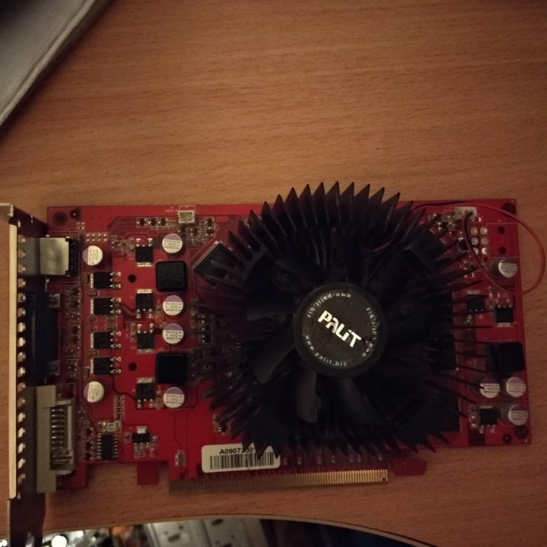
Noise levels
We measured noise levels on our test system, sitting on an open test bench, using an Extech model 407738 digital sound level meter. The meter was mounted on a tripod approximately 8″ from the test system at a height even with the top of the video card. We used the OSHA-standard weighting and speed for these measurements.
You can think of these noise level measurements much like our system power consumption tests, because the entire systems’ noise levels were measured. Of course, noise levels will vary greatly in the real world along with the acoustic properties of the PC enclosure used, whether the enclosure provides adequate cooling to avoid a card’s highest fan speeds, placement of the enclosure in the room, and a whole range of other variables. These results should give a reasonably good picture of comparative fan noise, though.
The GTS 250’s noise levels, both when idling and running a game, are some of the best we’ve measured in this round of tests. The new GeForce would look even better, relatively speaking, were it not up against some very quiet but essentially broken Asus custom coolers on the Radeon HD 4850 512MB.
Meanwhile, the strangely high noise levels for the Gigabyte Radeon HD 4850 1GB card, which match at idle and under load, are not a fluke. Although Gigabyte chose a nice, powerful Zalman cooler for this card, they did not see fit to endow this cooler with intelligent fan speed control. Or even kind-of-dumb fan speed control. In fact, there’s no fan speed control at all. When I asked Gigabyte why, the answer was: because this is an overclocked card. I wasn’t aware that eking out an additional 20MHz required the total destruction of a product’s acoustic profile, but that’s what’s happened here. And it’s a real shame. A real, puzzling shame.
GPU temperatures
I used GPU-Z to log temperatures during our load testing. In the case of multi-GPU setups, I recorded temperatures on the primary card.
With that fan spinning at 100% no matter what, the 4850 1GB certainly has some nice, low GPU temperatures. Meanwhile, the GTS 250 is easily quieter, but still keeps its temperatures well in check.
Conclusions
At this point in the review, Nvidia’s marketing department would no doubt like for me to say a few words about some of its key points of emphasis of late, such as PhysX, CUDA, and GeForce 3D Vision. I will say a few words, but perhaps not the words that they might wish.
CUDA is Nvidia’s umbrella term for accelerating non-graphics applications on the GPU, about which we’ve heard much lately. ATI Stream is AMD’s term for the same thing, and although we’ve heard less about it, it is very similar in nature and capability, as are the underlying graphics chips. In both cases, the first consumer-level applications for are only beginning to arrive, and they’re mostly video encoders that face some daunting file format limitations. Both efforts show some promise, but I expect that if they are to succeed, they must succeed together by running the same programs via a common programming interface. In other words, I wouldn’t buy one brand of GPU over the other expecting big advantages in the realm of GPU-compute capabilityespecially with a GPU as old as the G92 in the mix.
One exception to this rule may be PhysX, which is wholly owned by Nvidia and supported in games like Mirror’s Edge and… well, let me get back to you on that. I suspect PhysX might offer Nvidia something of an incremental visual or performance advantage in certain upcoming games, just as DirectX 10.1 might for AMD in certain others.
As for GeForce 3D Vision, the GeForce GTS 250 is purportedly compatible with it, but based on my experience, I would strongly recommend getting a much more powerful graphics card (or two) for use with this stereoscopic display scheme. The performance hit would easily swallow up all the GTS 250 has to giveand then some.
The cold reality here is that, for most intents and purposes, current GeForces and Radeons are more or less functionally equivalent, with very similar image quality and capability, in spite of their sheer complexity and rich feature sets. I would gladly trade any of Nvidia’s so-called “graphics plus” features for a substantial edge in graphics image quality or performance. The GTS 250 comes perilously close to losing out on this front due to the Radeon HD 4850’s superior performance with 8X multisampled antialiasing. The saving grace here is my affection for Nvidia’s coverage sampled AA modes, which offer similar image quality and performance.
All of which leads us to the inevitable price and performance comparison, and here, the GeForce GTS 250 offers a reasonably compelling proposition. This card replicates the functionality of the GeForce 9800 GTX+ in a smaller physical size, with substantially less power draw, at a lower cost. I like the move to 1GB of RAM, if only for the sake of future-proofing and keeping the door open to an SLI upgrade that scales well. In the majority of our tests, the GeForce GTS 250 proved faster than the Radeon HD 4850 1GB, if only slightly so. If the Radeon HD 4850 1GB were to stay at current prices, the GTS 250 would be the clear value leader in this segment.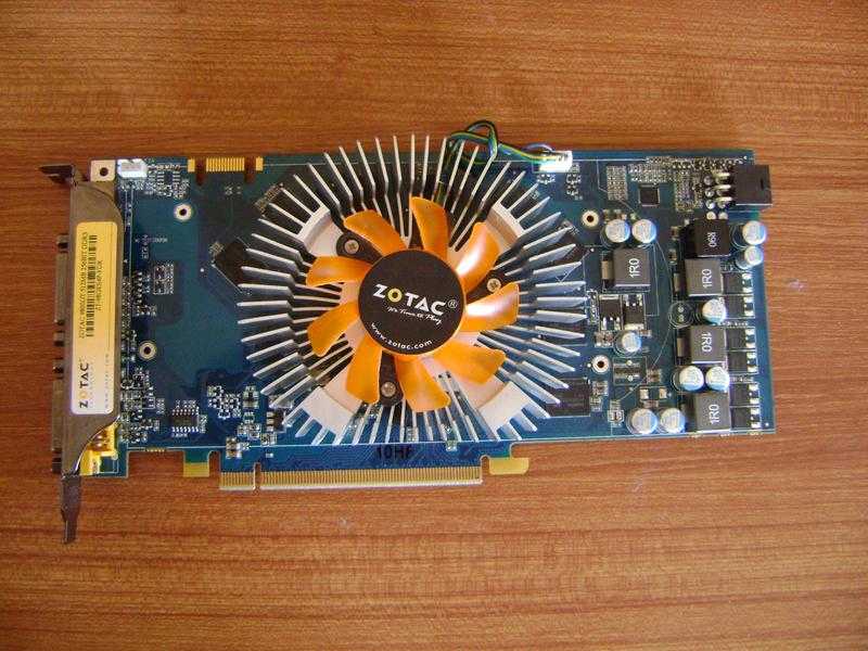
That’s apparently not going to happen, though. At the eleventh hour before publication of this review, AMD informed us of its intention to drop prices on several Radeon HD 4800 series graphics cards that compete in this general price range, mostly through a series of mail-in rebates. Some examples: this MSI 4850 512MB card starts at $159.99 and drops to $124.99 net via a mail-in rebate, and more intriguingly, this PowerColor 4870 512MB lists for $169.99 and has a $15 rebate attached, taking it to net price parity with the EVGA GTS 250 Superclocked card we tested. We hate mail-in rebates with a passion that burns eternal, but if these rebates were to last in perpetuity, the GeForce GTS 250 1GB at $149 nevertheless would be doomed.
For its part, Nvidia has indicated to us its resolve to be the price-performance leader in this portion of the market, so it may make an additional price move if necessary to defend its turf. Nvidia has limitations here that AMD doesn’t face, though, mainly because it doesn’t have the option of simply switching to GDDR5 memory to get twice the bandwidth.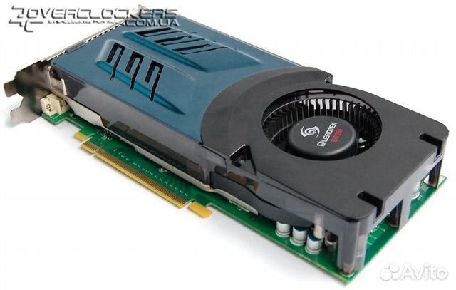 That is, after all, the only major difference between the Radeon HD 4850 and 4870. On the merits of its current GPU technology, AMD would seem to have the stronger hand.
What happens next is anybody’s guess. Just so long as Nvidia doesn’t rename this thing, I’ll be happy. There are GPU bargains ahead.
AMD Radeon R7 250 vs Nvidia GeForce GTS 450: What is the difference?
28points
AMD Radeon R7 250
36points
Nvidia GeForce GTS 450
vs
54 facts in comparison
AMD Radeon R7 250
Nvidia GeForce GTS 450
Why is AMD Radeon R7 250 better than Nvidia GeForce GTS 450?
- 217MHz faster GPU clock speed?
1000MHzvs783MHz - 0.17 TFLOPS higher floating-point performance?
0.77 TFLOPSvs0.6 TFLOPS - 1.74 GPixel/s higher pixel rate?
8 GPixel/svs6.26 GPixel/s - 41W lower TDP?
65Wvs106W - 248MHz faster memory clock speed?
1150MHzvs902MHz - 992MHz higher effective memory clock speed?
4600MHzvs3608MHz - 15.
 9GB/s more memory bandwidth?
73.6GB/svs57.7GB/s - 192 more shading units?
384vs192
Why is Nvidia GeForce GTS 450 better than AMD Radeon R7 250?
- 130million more transistors?
1170 millionvs1040 million - Supports multi-display technology?
- 8 more texture mapping units (TMUs)?
32vs24 - 8 more render output units (ROPs)?
16vs8 - Has Double Precision Floating Point (DPFP)?
- 1 more DVI outputs?
2vs1
Which are the most popular comparisons?
AMD Radeon R7 250
vs
Nvidia GeForce GTX 750 Ti
Nvidia GeForce GTS 450
vs
Nvidia GeForce GTX 550 Ti
AMD Radeon R7 250
vs
AMD Radeon RX 550
Nvidia GeForce GTS 450
vs
Nvidia GeForce 9800 GT
AMD Radeon R7 250
vs
Nvidia GeForce GT 1030 DDR4
Nvidia GeForce GTS 450
vs
Nvidia GeForce GTX 1050
AMD Radeon R7 250
vs
MSI GeForce GT 710 2GB
Nvidia GeForce GTS 450
vs
Nvidia GeForce GTX 460
AMD Radeon R7 250
vs
AMD Radeon R7 360
Nvidia GeForce GTS 450
vs
MSI GeForce GT 1030 2G LP OC
AMD Radeon R7 250
vs
Nvidia GeForce GTX 750
Nvidia GeForce GTS 450
vs
Nvidia GeForce GTX 560
AMD Radeon R7 250
vs
Gigabyte GeForce GT 630 2GB
Nvidia GeForce GTS 450
vs
Nvidia GeForce GTX 750
AMD Radeon R7 250
vs
Nvidia GeForce GTX 1050
Nvidia GeForce GTS 450
vs
Nvidia GeForce GT 520 (OEM)
AMD Radeon R7 250
vs
AMD Radeon Vega 8
Nvidia GeForce GTS 450
vs
Nvidia GeForce GT 640
Price comparison
User reviews
Overall Rating
AMD Radeon R7 250
0 User reviews
AMD Radeon R7 250
0. 0/10
0/10
0 User reviews
Nvidia GeForce GTS 450
2 User reviews
Nvidia GeForce GTS 450
10.0/10
2 User reviews
Features
Value for money
No reviews yet
10.0/10
1 votes
Gaming
No reviews yet
7.0/10
1 votes
Performance
No reviews yet
8.0/10
1 votes
Fan noise
No reviews yet
6.0/10
1 votes
Reliability
No reviews yet
9.0/10
1 votes
Performance
1.GPU clock speed
1000MHz
783MHz
The graphics processing unit (GPU) has a higher clock speed.
2.GPU turbo
1050MHz
Unknown. Help us by suggesting a value. (Nvidia GeForce GTS 450)
When the GPU is running below its limitations, it can boost to a higher clock speed in order to give increased performance.
3.pixel rate
8 GPixel/s
6.26 GPixel/s
The number of pixels that can be rendered to the screen every second.
4.floating-point performance
0.77 TFLOPS
0.6 TFLOPS
Floating-point performance is a measurement of the raw processing power of the GPU.
5.texture rate
24 GTexels/s
25.1 GTexels/s
The number of textured pixels that can be rendered to the screen every second.
6.GPU memory speed
1150MHz
902MHz
The memory clock speed is one aspect that determines the memory bandwidth.
7.shading units
Shading units (or stream processors) are small processors within the graphics card that are responsible for processing different aspects of the image.
8.texture mapping units (TMUs)
TMUs take textures and map them to the geometry of a 3D scene.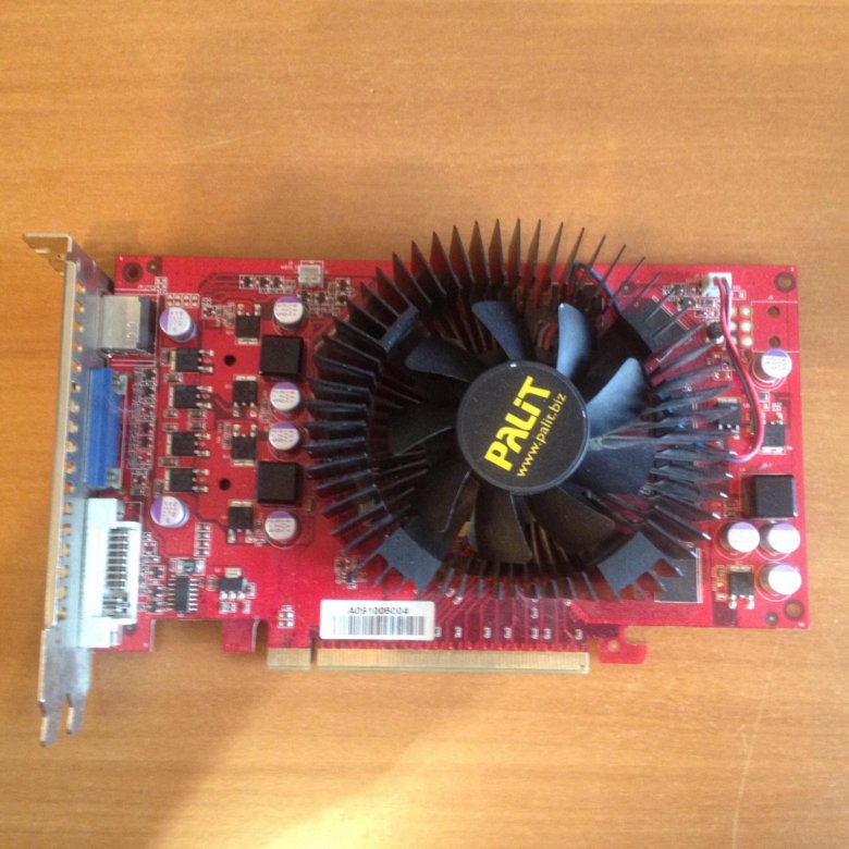 More TMUs will typically mean that texture information is processed faster.
9.render output units (ROPs)
The ROPs are responsible for some of the final steps of the rendering process, writing the final pixel data to memory and carrying out other tasks such as anti-aliasing to improve the look of graphics.
Memory
1.effective memory speed
4600MHz
3608MHz
The effective memory clock speed is calculated from the size and data rate of the memory. Higher clock speeds can give increased performance in games and other apps.
2.maximum memory bandwidth
73.6GB/s
57.7GB/s
This is the maximum rate that data can be read from or stored into memory.
3.VRAM
VRAM (video RAM) is the dedicated memory of a graphics card. More VRAM generally allows you to run games at higher settings, especially for things like texture resolution.
4.memory bus width
128bit
128bit
A wider bus width means that it can carry more data per cycle. It is an important factor of memory performance, and therefore the general performance of the graphics card.
5.version of GDDR memory
Newer versions of GDDR memory offer improvements such as higher transfer rates that give increased performance.
6.Supports ECC memory
✖AMD Radeon R7 250
✖Nvidia GeForce GTS 450
Error-correcting code memory can detect and correct data corruption. It is used when is it essential to avoid corruption, such as scientific computing or when running a server.
Features
1.DirectX version
DirectX is used in games, with newer versions supporting better graphics.
2.OpenGL version
OpenGL is used in games, with newer versions supporting better graphics.
3.OpenCL version
Some apps use OpenCL to apply the power of the graphics processing unit (GPU) for non-graphical computing. Newer versions introduce more functionality and better performance.
4.Supports multi-display technology
✖AMD Radeon R7 250
✔Nvidia GeForce GTS 450
The graphics card supports multi-display technology. This allows you to configure multiple monitors in order to create a more immersive gaming experience, such as having a wider field of view.
5.load GPU temperature
Unknown. Help us by suggesting a value. (AMD Radeon R7 250)
A lower load temperature means that the card produces less heat and its cooling system performs better.
6.supports ray tracing
✖AMD Radeon R7 250
✖Nvidia GeForce GTS 450
Ray tracing is an advanced light rendering technique that provides more realistic lighting, shadows, and reflections in games.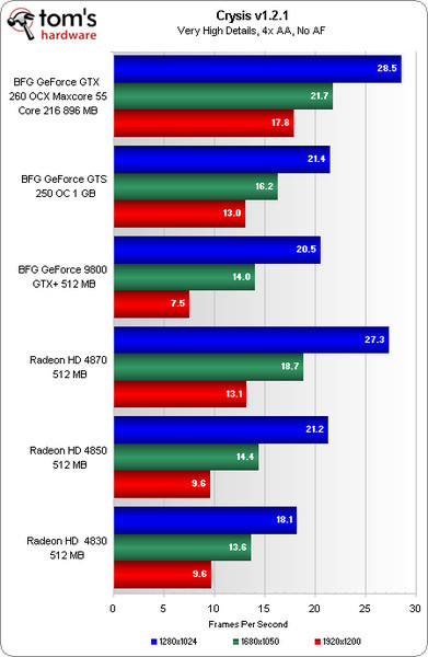
7.Supports 3D
✔AMD Radeon R7 250
✔Nvidia GeForce GTS 450
Allows you to view in 3D (if you have a 3D display and glasses).
8.supports DLSS
✖AMD Radeon R7 250
✖Nvidia GeForce GTS 450
DLSS (Deep Learning Super Sampling) is an upscaling technology powered by AI. It allows the graphics card to render games at a lower resolution and upscale them to a higher resolution with near-native visual quality and increased performance. DLSS is only available on select games.
9.PassMark (G3D) result
Unknown. Help us by suggesting a value. (AMD Radeon R7 250)
This benchmark measures the graphics performance of a video card. Source: PassMark.
Ports
1.has an HDMI output
✔AMD Radeon R7 250
✔Nvidia GeForce GTS 450
Devices with a HDMI or mini HDMI port can transfer high definition video and audio to a display.
2.HDMI ports
Unknown. Help us by suggesting a value. (AMD Radeon R7 250)
More HDMI ports mean that you can simultaneously connect numerous devices, such as video game consoles and set-top boxes.
3.HDMI version
Unknown. Help us by suggesting a value. (AMD Radeon R7 250)
Unknown. Help us by suggesting a value. (Nvidia GeForce GTS 450)
Newer versions of HDMI support higher bandwidth, which allows for higher resolutions and frame rates.
4.DisplayPort outputs
Allows you to connect to a display using DisplayPort.
5.DVI outputs
Allows you to connect to a display using DVI.
6.mini DisplayPort outputs
Allows you to connect to a display using mini-DisplayPort.
Price comparison
Cancel
Which are the best graphics cards?
Sparkle GeForce GTS 250 1GB Graphics Card
The GTS 250 shares the same GPU core as the 9800 GTX+, a midrange gaming graphics card. Though the core is unchanged, the PCB has undergone some revision, perhaps to reduce power consumption. That could be one explanation for the smaller heatsink atop Sparkle’s 1GB version of the GTS 250.
Mar. 30, 2009 by Lawrence Lee
|
Product |
Sparkle GeForce GTS 250 1GB |
|
Manufacturer |
Sparkle |
|
Street Price |
~US$150 |
nVidia has received a lot of flak for their newest GPU, the GeForce GTS 250.
The name would seem to indicate a slightly cut-down version of the GTX 260,
but it is a simple renaming of the 9800 GTX+, a midrange gaming card marketed
to compete against ATI’s Radeon
HD 4850. Revising nomenclature is nothing new to nVidia, after all the
entire 9800 series was fabricated out of the 8800 series. The 9800 GT is actually
a 8800GT and the 9800 GTX+, is an overclocked 9800 GTX, which in-turn is a really
a G92 8800 GTS. With the economic climate worsening and demand for high-end
graphics dwindling, there’s no telling how many more times nVidia will recycle
the venerable G92 core.
While nVidia did not touch the GPU core, the PCB has undergone some changes.
There are two different GTS 250 board designs floating around — one is 9″
long with a single power connector, while the second is 9.5″ long with
two power connectors. The reference 9800 GTX+ is 10.5″ long so some changes,
probably to power regulation have been implemented, even if the core itself
has been left untouched. The 250 is also available with three different memory
sizes: 512MB, 1GB, and a whopping 2GB.
|
|
The card we’re examining is made by Sparkle Computer — not in any way
related to Sparkle Power. Not a huge name in the industry, Sparkle Computer
seems to focus their sole attention on producing graphics cards.
|
|
Our sample is a 1GB model with a native HDMI port, though a S/PDIF cable is
still required to patch through audio. The card is equipped with a uniquely
designed heatsink rather than the common all-encompassing box coolers residing
on most GTS 250s and GTX series cards.
|
Sparkle GeForce GTS 250 1GB: Specifications |
|
| Model number | SXS2501024D3-NM |
| Graphics Processing | NVIDIA GeForce GTS250 |
| Stream Processors | 128 |
| Core Clock | 738MHz |
| Memory Clock | 2200MHz |
| Memory Type | 1024MB GDDR3 |
| Memory Interface | 256Bit |
| Shader Clock | 1836MHz |
| Bus Type | PCI-Express 2. 0 0 |
| RAMDAC | 400 MHz |
|
|
According to GPU-Z, our GTS 250 sample shares the same number of shaders and
core/memory/shader frequency as a reference 9800 GTX+. Nothing surprising here.
PHYSICAL DETAILS
|
|
|
|
 1 cm. On the top side
|
|
|
|
THE COOLER & INSTALLATION
Note that all testing on the card was performed before the cooler was removed.
Warning — removing the heatsink from a card generally voids the product’s
warranty. Do so at your own risk.
|
|
 The mounting holes form a 53.5 mm square around the
|
|
|
|
|
|
TEST METHODOLOGY
Our test procedure is an in-system test, designed to:
1. Determine whether the card’s cooler is adequate for use in a low-noise system.
By adequately cooled, we mean cooled well enough that no misbehavior
related to thermal overload is exhibited. Thermal misbehavior in a graphics
card can show up in a variety of ways, including:
- Sudden system shutdown, bluescreen or reboot without warning.
- Jaggies and other visual artifacts on the screen.
- Motion slowing and/or screen freezing.
Any of these misbehaviors are annoying at best and dangerous at worst —
dangerous to the health and life span of the graphics card, and sometimes to
the system OS.
2. Estimate the card’s power consumption. This is a good indicator of how efficient
the card is and will have an effect on how hot the stock cooler becomes due
to power lost in the form of heat. The lower the better.
3. Determine the card’s ability to play back high definition video, to see
if whether it is a suitable choice for a home theater PC.
Test Platform
- Intel
Pentium D 930 Presler core processor. Official TDP of 95W. - AOpen
i945Ga-PHS motherboard – Intel i945Ga Chipset; built-in VGA. - Gigabyte G-Power 2 Pro
heatsink, modified with a Scythe
Slip Stream 500RPM 120mm fan. - Corsair
XMS2 memory 1GB, DDR2-800 - Seagate Momentus 5400.3
160 GB, 5400RPM, ATA/100, 2-platter notebook hard drive, suspended - Seasonic S12-600
ATX12V v2.0 compliant power supply, modified with a Scythe
Slip Stream 800RPM 120mm fan @ 5V. - Antec P180B case,
modified in detail below. - Nexus 120mm
fan connected to a variable fan speed controller. - Microsoft
Windows XP Professional operating system - nVidia
Forceware 182.08 graphics driver
Measurement and Analysis Tools
Testing Procedures
Our first test involves recording the system power consumption using a Seasonic
Power Angel as well as CPU and GPU temperatures using SpeedFan and GPU-Z during
different states: Idle, under load with CPUBurn running to stress the processor,
and with CPUBurn and ATITool’s artifact scanner (or FurMark — whichever produces
higher power consumption) running to stress both the CPU and GPU simultaneously.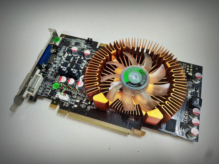
This last state mimics the stress on the CPU and GPU produced by a modern video
game. The software is left running until the GPU temperature remains stable
for at least 10 minutes. If artifacts are detected by ATITool or any other instability
is noted, the heatsink is deemed inadequate to cool the video card in our test
system.
If the heatsink has a fan, the load state tests are repeated at various fan
speeds while the system case fan is left at its lowest setting of 7V. If the
card utilizes a passive cooler, the system fan is varied instead to study the
effect of system airflow on the heatsink’s performance. System noise measurements
are made at each fan speed.
Power consumption is also measured during playback of a variety of video clips
with PowerDVD to test the efficiency of the card’s H.264/VC-1 hardware acceleration.
Video Test Suite
|
1080p | 24fps | ~10mbps |
H. |
 264:
264:
|
1080p | 24fps | ~8mbps |
WMV-HD: |
|
1080p | 24fps | ~19mbps |
VC-1: Drag Race is a recording of a scene from |
Estimating DC Power
The following power efficiency figures were obtained for the
Seasonic S12-600
used in our test system:
|
Seasonic S12-500 / 600 TEST RESULTS |
||||||
|
DC Output (W) |
65. |
89.7 |
148.7 |
198.5 |
249.5 |
300.2 |
|
AC Input (W) |
87.0 |
115.0 |
183.1 |
242.1 |
305.0 |
370.2 |
|
Efficiency |
75.1% |
78.0% |
81.2% |
82.0% |
81.8% |
81.1% |
 3
3This data is enough to give us a very good estimate of DC demand in our
test system. We extrapolate the DC power output from the measured AC power
input based on this data. We won’t go through the math; it’s easy enough
to figure out for yourself if you really want to.
TEST RESULTS
BASELINE, with Integrated Graphics: To establish a baseline, we measured
the power consumption of our test system using integrated graphics, at both
idle and while stressed with CPUburn
|
VGA Test Bed: Baseline Results |
|||
|
System |
CPU |
System Power |
|
|
AC |
DC (Est. |
||
|
Idle |
22°C |
73W |
Unknown |
|
CPUBurn |
39°C |
144W |
115W |
|
Ambient temperature: 21°C |
|||
 )
)Sparkle GeForce GTS 250 1GB:
|
VGA Test Bed: Sparkle GeForce GTS 250 1GB |
||||||
|
System |
VGA Fan Speed |
SPL |
GPU |
CPU |
System Power |
|
|
AC |
DC (Est. |
|||||
|
Idle |
35% |
14 dBA |
40°C |
23°C |
97W |
74W |
|
CPUBurn |
40°C |
41°C |
170W |
137W |
||
|
CPUBurn + ATITool |
63% |
24 dBA |
73°C |
49°C |
246W |
202W |
|
CPUBurn + FurMark |
86% |
27 dBA |
84°C |
52°C |
292W |
239W |
|
Ambient temperature: 21°C. |
||||||
 )
)
The Sparkle GeForce GTS 250 acoustics were more or less like a typical midrange
graphics card. Idle, it was fairly quiet, increasing the measured SPL of our
test system by only 2 dB, though it did hum and click somewhat. Luckily, much
of this was masked once behind the case’s side panel. Upon stress, the fan sped
up almost immediately, becoming increasingly buzzy and whiny. The system noise
level topped out an annoying 27 dBA with CPUBurn and FurMark running.
The heatsink kept the GPU very cool, reaching a maximum of just 73°C when
stressed with ATITool. We would have preferred the fan not spin quite so fast,
as temperatures in the low 80’s are perfectly acceptable in our book. When stressed
with FurMark, the GPU temperature maxed out at 84°C and the system power
consumption neared 300W AC.
Fan Control
Our sample did not ship with any utility for monitoring or fan control. For
those who wish to control the fan’s speed directly, it is possible to do so
with RivaTuner.
|
RivaTuner: Fan control tab. |
While the fan’s speed can be manipulated in a linear progression between 35%
and 100% with RivaTuner, actually there are only three or four ‘stages’ of fan
speed. For example, the 35% and 40% setting sound identical — the fan speed
does not actually change until it is set past a threshold. By contrast, the
card’s automatic fan control has a smoother, more extensive range.
POWER
The power consumption of an add-on video card can be estimated by comparing
the total system power draw with and without the card installed. Our results
were derived thus:
1. Power consumption of the graphics card at idle – When CPUBurn is
run on a system, the video card is not stressed at all, and stays in idle mode.
This is true whether the video card is integrated or an add-on PCIe 16X device.
Hence, when the power consumption of the base system under CPUBurn is subtracted
from the power consumption of the same test with the graphics card installed,
we obtain the increase in idle power of the add-on card over the
integrated graphics chip (Intel GMA950). (The actual idle power
of the add-on card cannot be derived, because the integrated graphics does draw
some power — we’d guess no more than a watt or two.)
2. Power consumption of the graphics card under load – The power draw
of the system is measured with the add-on video card, with CPUBurn and FurMark
running simultaneously. Then the power of the baseline system (with integrated
graphics) running just CPUBurn is subtracted. The difference is the load power
of the add-on card. (If you want to nitpick, the 1~2W power of the integrated
graphics at idle should be added to this number.) Any load on the CPU from FurMark
should not skew the results, since the CPU was running at full load in both
systems.
Both results are scaled by the efficiency of the power supply (tested
here) to obtain a final estimate of the DC power consumption.
|
Power Consumption Comparison (DC) |
|||
|
Card |
Est. |
Est. Power (ATITool) |
Est. Power (FurMark) |
|
Asus EN9800GT 512MB |
32W |
72W |
80W |
|
ATI HD 4830 512MB* |
18W |
80W |
87W |
|
Sparkle GTS 250 1GB |
22W |
87W |
124W |
|
Diamond HD 4850 512MB |
50W |
101W |
N/A |
|
Asus ENGTX260 896MB |
35W |
122W |
N/A |
|
ATI HD 4870 1GB |
67W |
121W |
134W |
|
* sample with unknown number of stream processors |
|||
 Power (Idle)
Our Sparkle GTS 250 1GB sample exhibited relatively low idle power consumption
compared to other gaming-oriented cards. Among tested card the same league,
only our HD 4830 sample consumed
less power when the system is idle, and even then only 4W less. When stressed
however, the GTS 250 can use as much as 124W DC by our estimates.
|
Video Playback Power Consumption (AC) |
|||
|
Card |
Rush Hour |
Coral Reef |
Drag Race |
|
Asus EN9800GT 512MB |
119W |
127W |
141W |
|
ATI HD 4830 512MB* |
131W |
139W |
153W |
|
Sparkle GTS 250 1GB |
133W |
136W |
164W |
|
Diamond HD 4850 512MB |
123W |
134W |
160W |
|
Asus ENGTX260 896MB |
136W |
151W |
176W |
|
ATI HD 4870 1GB |
183W |
176W |
199W |
|
* sample with unknown number of stream processors |
|||
For video playback, the faster 3D cards all draw relatively high power. The
GTS 250 holds its own against its main rival, the HD
4850. In the big picture, this probably isn’t going to sway any gamer
to one card or another. The faster the card, the more power its going to draw,
whether during video playback or intense gaming.
MP3 SOUND RECORDINGS
These recordings were made with a high
resolution, lab quality, digital recording system inside SPCR’s
own 11 dBA ambient anechoic chamber, then converted to LAME 128kbps
encoded MP3s. We’ve listened long and hard to ensure there is no audible degradation
from the original WAV files to these MP3s. They represent a quick snapshot of
what we heard during the review.
These recordings are intended to give you an idea of how the product sounds
in actual use — one meter is a reasonable typical distance between a computer
or computer component and your ear. The recording contains stretches of ambient
noise that you can use to judge the relative loudness of the subject. Be aware
that very quiet subjects may not be audible — if we couldn’t hear it from
one meter, chances are we couldn’t record it either!
The recording starts with 5~10 seconds of room ambiance, followed by 5~10 seconds
of the VGA test system without a video card installed, and then the actual product’s
noise at various levels. As this particular card did not add any noise the test
system, we have provided only a recording of the test system with its system
fan set to the levels tested. For the most realistic results, set the
volume so that the starting ambient level is just barely audible, then don’t
change the volume setting again.
- Sparkle
GeForce GTS 250 1GB fan at one meter
— idle (35% / 14 dBA@1m)
— load (86% / 27 dBA@1m)
FINAL THOUGHTS
Gaming: Please check out the gaming-oriented reviews of the GTS 250
1GB at Tech
Report, techPowerUp,
and Legit
Reviews, The general consensus is that it is more or less equivalent
to the HD 4850, and offers slightly better performance than the 512MB version
of the GTS 250/9800 GTX+ when image quality settings and resolution are cranked
up.
Cooling/Noise: The cooler employed by Sparkle does an adequate job
cooling the GPU. It is practically inaudible when idle, but when the fan speed
increases under load, it becomes too loud for SPCR. This is classic low-cost,
brute-force fan cooling: A fan that spins fast enough is a cheaper alternative
to a larger, more costly heatsink. Most of the contemporary graphics cards we’ve
tested in the past year or so, the HD 4830/4850/4870
and GTX 260 for example,
all generate less noise on full load than the Sparkle GTS 250. The heatsink
seems too small to cool the card effectively unless the fan speed is cranked
up.
Power Consumption: By our estimates, the Sparkle GeForce GTS 250 1GB
requires approximately 22W when idle and up to 124W DC when stressed to the
limit. The idle figure is impressively low for a card of the GTS 250’s caliber.
The load figure is more or less what you’d expect given the 3D performance.
It should also be noted that our sample is 9.5″ long with two power connectors,
while some GTS 250’s are 0.5″ shorter with only one power connector. These
slimmed down versions may be even more power efficient.
Overall, the Sparkle GeForce GTS 250 1GB is a good midrange graphics card with
a competitive price-point to battle the Radeon HD 4850. It has a native HDMI
port (though a S/PDIF feed is needed for audio) and it is very quiet and power
efficient when idle. Once the GPU is stressed, however, the fan kicks into overdrive
to compensate for the undersized heatsink, making it unsuitable for any silent/quiet
PC. Among GTS 250 variants, this one may have the dubious distinction of the
cooler with the smallest surface area. With such a small heatsink on a card
that can draw more than 120W of power, it’s no wonder that the fan has to ramp
up to high speed under load. For silent PC gamers, a better aftermarket heasink/fan
replacement is probably mandatory with this Sparkle.
|
Sparkle GeForce GTS 250 1GB |
|
| PROS
* Quiet when idle |
CONS
* Heatsink too small; has a loud fan to compensate |
Our thanks to Sparkle
Computer for the
video card sample.
* * *
Articles of Related Interest
Asus EN9400GT Silent Edition
Asus
Radeon HD 4870 Matrix
PowerColor SCS HD4650: A Fanless Budget Graphics Card
Asus
EN9800GT Matrix Edition
Filling
the Gap: ATI Radeon HD 4830
Redefining Budget Gaming Graphics: ATI’s
HD 4670
Asus ENGTX260: A Quiet Graphics
Card for Gamers?
* * *
Discuss this article in the
SPCR forums.
EVGA GeForce GTS 250 Superclocked – Techgage
It’s been well over eight months since NVIDIA first launched their GeForce 200 series, and until now, we haven’t seen much from the company in way of mid-range offerings. The closest we’ve come has been with the GTX 260, but at over $200 (much more at launch), it’s still more than some people will want to spend. We can stop waiting for such a thing to arrive though, as the GTS 250 makes its entrance now.
The lead up to this card’s launch has been a little different than most, though, as rumors and speculation of what the card is all about have been soaring through the Internet for the past few weeks. Some of the points made have been valid, some have been false, but if anything’s true, it’s that NVIDIA definitely caught the attention of enthusiasts with this one.
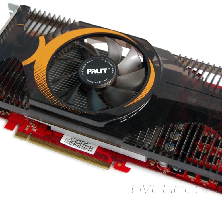
To kick things off, let’s figure out what this card is, and what it isn’t. As rumors have been clear to point out, the GTS 250 utilizes NVIDIA’s G92b core, which is the exact same chip used in their 9800 GTX+. It’s for that reason that some have been quick to throw a quick jab at NVIDIA, since the origin of this GPU was the 65nm G92 – first found in the 8800 GT. Realizing that, it becomes a little easier to understand why some are up in arms.
For the most part, I don’t really blame anyone. I’d like to see a brand-new mid-range core as much as the next guy. But for what it’s worth, NVIDIA isn’t trying to hide anything, and they’ve done well to fully disclose exactly what the GTS 250 is. So, the important thing to note is that they’re not trying to fool anyone into thinking this is something that it’s not, although some may disagree.
Closer Look at NVIDIA’s GeForce GTS 250
What’s going on, then? As pointed out during a press briefing last week, NVIDIA discussed their desire to “simplify” their product line-up. One example used to explain the situation was to take a look at the card that the GTS 250 replaces. At quick glance, a regular consumer may assume that a 9800 GTX+ is much more powerful than, say, a GTX 285, when their performance is in fact on opposite sides of the spectrum. Hence, the need to simplify comes into play.
Throughout the coming year, the company will target their entire current line-up and rename models appropriately, so that when consumers go into a retailer or hop onto an e-tailer, they’ll feel confident in their purchasing decision (although, that would also assume they visited our site first!). Current naming schemes are a real problem, but not only with GPUs. Currently, AMD’s own processors are about to hit the “10K” mark, and Intel hit it not long ago, hence the revised naming scheme for their Core i7 line-up. So, any advances made to simplify product naming schemes is fine by me.
To reiterate, the GTS 250 = 9800 GTX+ in almost all regards, except for some that I’ll talk about now. First, thanks to a board redesign, NVIDIA has shortened the card an entire inch, to settle in at 9″. The GTX 285, by comparison, is 10.5″, so the smaller body of this card will be appreciated by those with a smaller chassis. Also thanks to this board redesign, one power connector was removed, so all you need to power the GTS 250 is a single 6-Pin PCI-E and you’re good to go. Despite these changes though, the TDP is 5W higher on the GTS 250, at 150W.
Another advantage to the GTS 250 is the increase in memory size, to 1GB. The 9800 GTX+ was limited to 512MB, so without even testing, we can be assured that the newer card will fare a bit better in high-resolution gaming (1920×1200+). That said, there will also be a 512MB version of the GTS 250 available, which is ideal for those who want to pair it with their already-existing 9800 GTX+ for SLI. Since the architecture is the same, SLI will work fine as long as the memory densities are the same.
Finally pricing for the GTS 250 1GB is $149, while the GTS 250 512MB will debut at $129. The latter is quite similar to current 9800 GTX+ pricing, although some of those may be had for even less after mail-in rebates. The competition that the GTS 250 goes after is ATI’s Radeon HD 4850 1GB, a card that at recent check, retails for at least $30 more (before mail-in-rebates).
| GTX 295 |
576 |
1242 |
1000 |
1792MB |
448-bit |
480 |
| GTX 285 |
648 |
1476 |
1242 |
1GB |
512-bit |
240 |
| GTX 280 |
602 |
1296 |
1107 |
1GB |
512-bit |
240 |
| GTX 260/216 |
576 |
1242 |
999 |
896MB |
448-bit |
216 |
| GTX 260 |
576 |
1242 |
999 |
896MB |
448-bit |
192 |
| GTS 250 |
738 |
1836 |
1100 |
1GB |
256-bit |
128 |
| 9800 GX2 |
600 |
1500 |
1000 |
1GB |
512-bit |
256 |
| 9800 GTX+ |
738 |
1836 |
1100 |
512MB |
256-bit |
128 |
| 9800 GTX |
675 |
1688 |
1100 |
512MB |
256-bit |
128 |
| 9800 GT |
600 |
1500 |
900 |
512MB |
256-bit |
112 |
| 9600 GT |
650 |
1625 |
900 |
512MB |
256-bit |
64 |
| 9600 GSO |
550 |
1375 |
800 |
384MB |
192-bit |
96 |
Below, you can see the card’s status report courtesy of the latest version of GPU-Z. Everything here is accurate, aside from the GPU code name and manufacturing process. As already mentioned, this card uses the G92b core, which is built on a 55nm process, not a 65nm one as it appears in the shot. Also seen here are the 128 Shader (or CUDA) processors and 16 ROP units. Overall, the card may be “outdated” by some standards, but it’s still a solid offering for the price, which is the most important thing.
The GTS 250 also features a rather familiar design, one that’s similar for the most part to the GTX 200 cards before it, but smaller. One noticeable difference is that the glossiness of the higher-end cards is lost, replaced with a matte surface (which I actually prefer). Also, despite the card’s budget pricing, you are able to hook three of these guys together for Tri-SLI. It would be an odd route to take (as opposed to purchasing a larger card to begin with), but having the option doesn’t hurt.
Taking a look at the opposite side of the card, we can see the lone PCI-E 6-Pin connector, and also have a good view of the fan. The cooler design is simple in general, but pretty efficient for a stock offering. There’s no doubt that GPU vendors will follow-up to this launch with their own cooler designs, however, which tend to be much better for overclocking and temperatures in general.
You can expect that all of the launch GTS 250’s will look identical, save for the vendor sticker, but similar to the case of our EVGA card here, pre-overclocked models are also sure to be plentiful.
Before we dive into our testing results, one thing I wanted to point out was that while NVIDIA believes the GTS 250’s main competition is ATI’s Radeon HD 4850 1GB, we didn’t have one on hand, to use for the sake of comparison. Also, due to time constraints, we were unable to put the 512MB variant through our most-recent test suite. However, since that’s a 512MB version, the comparison doesn’t matter a great deal at this point. A more appropriate comparison would be with the 9800 GTX+ 512MB, which we do have results for.
So let’s get to it! On the next page, we have our test setup and methodology explained in some depth, and following that, we’ll get right into our Call of Duty: World at War results.
Support our efforts! With ad revenue at an all-time low for written websites, we’re relying more than ever on reader support to help us continue putting so much effort into this type of content. You can support us by becoming a Patron, or by using our Amazon shopping affiliate links listed through our articles. Thanks for your support!
Remixing the G92 — NVIDIA GeForce GTS 250
?>
Trending
ScamShield now available for Android users
Apple reportedly cancelled plan to increase iPhone 14 production
Product Listing
- News
- Reviews & Articles
-
Page 1 of 9 — Old Habits Die HardPage 2 of 9 — The ASUS GeForce GTS 250Page 3 of 9 — Test SetupPage 4 of 9 — Windows Vista Results — 3DMark06Page 5 of 9 — Windows Vista Results — 3DMark VantagePage 6 of 9 — Windows Vista Results — Crysis Warhead and Far Cry 2Page 7 of 9 — Windows Vista Results — Unreal Tournament 3Page 8 of 9 — Temperature, Power Consumption & OverclockingPage 9 of 9 — Conclusion
Page 1 of 9 — Old Habits Die Hard
- Next >
Old Habits Die Hard
They say an elephant never forgets and a leopard never changes its spots. So it should come as no surprise then that NVIDIA, so fond of renaming, rehashing and rebranding their products, has gone back to its old ways. And we are disappointed. Before CeBIT, rumors were rife about a new NVIDIA SKU and many speculated that the graphics giant has finally managed to scale its high-end GTX 200 down a notch to create mainstream, entry-level variants of GTX 200 cards. On the other hand, there were also rumors that they were going to rehash one of the older SKUs so that, you know, it’ll appear to be new?
Unfortunately, NVIDIA has once again decided to opt for the easy way out. The latter rumor proved to be true and the brand ‘new’ GeForce GTS 250 that you see here has a GeForce 9800 GTX+ GPU core at its heart.
If you’ve already forgotten, the GeForce 9800 GTX+ was launched last year in June and it was itself a quick fix solution to ATI’s Radeon HD 4850. In fact, the GeForce 9800 GTX+ is a refresh of the even older GeForce 9800 GTX based on the G92 and only differs from the latter in that it is manufactured using a 55nm process and is therefore able to accommodate higher clock speeds. One can hence trace the roots of this GeForce GTX 250 back to the venerable G80 architecture that debuted in the GeForce 8800 GTX in 2006.
In the case of the GeForce GTS 250, it differentiates itself from the GeForce 9800 GTX+ in that it comes in both 512MB and 1GB flavors. 1GB, NVIDIA claims, will offer better performance with anti-aliasing switched on. Also, it requires only a single 6-pin power connector to power up, as opposed to two for the GeForce 9800 GTX+. The PCB of the new card is also slightly shorter by an inch, which means a lower manufacturing cost for NVIDIA. As for clock speeds, they don’t differ one bit from the GeForce 9800 GTX+, which means 738MHz at the core, 2200MHz DDR for the memory and 1836MHz for the shaders.
| Model | NVIDIA GeForce GTS 250 1GB | NVIDIA GeForce 9800GTX+ 512MB | NVIDIA GeForce 9800GTX 512MB | ATI Radeon HD 4850 512MB |
|---|---|---|---|---|
| Core Code | G92 | G92 | G92 | RV770 |
| Transistor Count | 754 million | 754 million | 754 million | 965 million |
| Manufacturing Process | 55nm | 55nm | 65nm | 55nm |
| Core Clock | 738MHz | 738MHz | 675MHz | 625MHz |
| Stream Processors | 128 Stream Processors | 128 Stream Processors | 128 Stream Processors | 160 Processors (800 Stream Processing Units) |
| Stream Processor Clock | 1836MHz | 1836MHz | 1688MHz | 625MHz |
| Texture Mapping Units (TMU) or Texture Filtering (TF) units | 64 | 64 | 64 | 40 |
| Raster Operator units (ROP) | 16 | 16 | 16 | 16 |
| Memory Clock | 2200MHz GDDR3 | 2200MHz GDDR3 | 2200MHz GDDR3 | 2000MHz GDDR3 |
| DDR Memory Bus Width | 256-bit | 256-bit | 256-bit | 256-bit |
| Memory Bandwidth | 70. |
70.4GB/s | 70.4GB/s | 64.0GB/s |
| PCI Express Interface | PCIe ver 2.0 x 16 | PCIe ver 2.0 x 16 | PCIe ver 2.0 x 16 | PCIe ver 2.0 x16 |
| Molex Power Connectors | 1 x 6-pin | 2 x 6-pin | 2 x 6-pin | 1 x 6-pin |
| CMulti GPU Technology | SLI | SLI | SLI | CrossFireX |
| DVI Output Support | 2 x Dual-Link | 2 x Dual-Link | 2 x Dual-Link | 2 x Dual-Link |
| HDCP Output Support | Yes | Yes | Yes | Yes |
| Street Price | US$129 / US$149 | ~US$179 | ~US$159 | ~US$169 |
-
Page 1 of 9 — Old Habits Die HardPage 2 of 9 — The ASUS GeForce GTS 250Page 3 of 9 — Test SetupPage 4 of 9 — Windows Vista Results — 3DMark06Page 5 of 9 — Windows Vista Results — 3DMark VantagePage 6 of 9 — Windows Vista Results — Crysis Warhead and Far Cry 2Page 7 of 9 — Windows Vista Results — Unreal Tournament 3Page 8 of 9 — Temperature, Power Consumption & OverclockingPage 9 of 9 — Conclusion
Page 1 of 9 — Old Habits Die Hard
- Next >
Join HWZ’s Telegram channel here and catch all the latest tech news!
Our articles may contain affiliate links. If you buy through these links, we may earn a small commission.
Sponsored Links
Compare NVIDIA GeForce GTS 250 and NVIDIA GeForce 9800 GT
Comparative analysis of NVIDIA GeForce GTS 250 and NVIDIA GeForce 9800 GT video cards by all known characteristics in the categories: General information, Specifications, Video outputs and ports, Compatibility, dimensions, requirements, API support, Memory, Technology support.
Analysis of video card performance by benchmarks: PassMark — G3D Mark, PassMark — G2D Mark, GFXBench 4.0 — Manhattan (Frames), GFXBench 4.0 — Manhattan (Fps), GFXBench 4.0 — T-Rex (Frames), GFXBench 4.0 — T-Rex (Fps) ).
NVIDIA GeForce GTS 250
versus
NVIDIA GeForce 9800 GT
Advantages
reasons to choose NVIDIA GeForce GTS 250
- The VEALLEMENT DIFFERENCE, the difference in the production dates of 7 MONTH (S)
- The nucleus frequency is about 22% more: 1836 MHZ 1500 MHZ
- 40% more texturing speed: 47.
2 billion / sec vs 33.6 billion / sec
- 14% more shader processors: 128 vs 112
- 15% better floating point performance: 387.1 gflops vs 336.0 gflops
- A newer graphics card production process allows it to be more powerful, but with lower power consumption: 55 nm vs 65 nm
- Maximum memory size is 2 times larger ( a): 1 GB vs 512 MB
- 22% more memory frequency: 1100 MHz vs 900 MHz
- Approximately 29% more performance in PassMark — G3D Mark benchmark: 621 vs 480
- Performance in PassMark — G2D Mark benchmark approx. 2% more: 84 vs 82
- About 9% more performance in GFXBench 4.0 — Manhattan (Frames) benchmark: 3108 vs 2845
- About 9% more performance in GFXBench 4.0 — Manhattan (Fps) benchmark: 3108 vs 2845
- GFX benchmark4 — benchmark performance T-Rex (Frames) about 1% more: 3351 vs 3304
- GFXBench 4.0 performance — T-Rex (Fps) about 1% more: 3351 vs 3304
| Release date | 4 March 2009 vs 21 July 2008 |
| Core frequency | 1836 MHz vs 1500 MHz |
| Texturing speed | 47. |
| Number of shaders | 128 vs 112 |
| Floating point performance | 387.1 gflops vs 336.0 gflops |
| Process | 55 nm vs 65 nm |
| Maximum memory size | 1 GB vs 512 MB |
| Memory frequency | 1100 MHz vs 900 MHz |
| PassMark — G3D Mark | 621 vs 480 |
| PassMark — G2D Mark | 84 vs 82 |
| GFXBench 4.0 — Manhattan (Frames) | 3108 vs 2845 |
| GFXBench 4. |
3108 vs 2845 |
| GFXBench 4.0 — T-Rex (Frames) | 3351 vs 3304 |
| GFXBench 4.0 — T-Rex (Fps) | 3351 vs 3304 |
Reasons to choose NVIDIA GeForce 9800 GT
- About 43% less power consumption: 105 Watt vs 150 Watt
| Power consumption (TDP) | 105 Watt vs 150 Watt |
Benchmark comparison
GPU 1: NVIDIA GeForce GTS 250
GPU 2: NVIDIA GeForce 9800 GT
| PassMark — G3D Mark |
|
|||
| PassMark — G2D Mark |
|
|||
| GFXBench 4. |
|
|||
| GFXBench 4.0 — Manhattan (Fps) |
|
|||
| GFXBench 4.0 — T-Rex (Frames) |
|
|||
| GFXBench 4.0 — T-Rex (Fps) |
|
| Name | NVIDIA GeForce GTS 250 | NVIDIA GeForce 9800 GT |
|---|---|---|
| PassMark — G3D Mark | 621 | 480 |
| PassMark — G2D Mark | 84 | 82 |
| GFXBench 4. |
3108 | 2845 |
| GFXBench 4.0 — Manhattan (Fps) | 3108 | 2845 |
| GFXBench 4.0 — T-Rex (Frames) | 3351 | 3304 |
| GFXBench 4.0 — T-Rex (Fps) | 3351 | 3304 |
Performance comparison
| NVIDIA GeForce GTS 250 | NVIDIA GeForce 9800 GT | |
|---|---|---|
| Architecture | Tesla | Tesla |
| Codename | G92B | G92 |
| Production date | March 4, 2009 | July 21, 2008 |
| Price at first issue date | $199 | $160 |
| Ranking | 956 | 1007 |
| Price now | $114. |
$103.99 |
| Type | Desktop | Desktop |
| Price/performance ratio (0-100) | 9.91 | 8.86 |
| Core frequency | 1836MHz | 1500MHz |
| Number of CUDA conveyors | 128 | 112 |
| Floating point performance | 387.1 gflops | 336.0 gflops |
| Process | 55nm | 65 nm |
| Maximum temperature | 105 °C | 105 °C |
| Number of shaders | 128 | 112 |
| Texturing speed | 47. |
33.6 billion/sec |
| Power consumption (TDP) | 150 Watt | 105 Watt |
| Number of transistors | 754 million | 754 million |
| Audio input for HDMI | S/PDIF | S/PDIF |
| Video connectors | 2x DVI, Two Dual Link DVI | 2x DVI, 1x S-Video, HDTVDual Link DVI |
| HDMI | ||
| Maximum resolution VGA | 2048×1536 | 2048×1536 |
| Multi-monitor support | ||
| Height | 4. |
|
| Interface | PCIe 2.0 x16 | PCIe 2.0 x16 |
| Length | 9″ (228.6 mm) (22.9 cm) | 9″ (22.9cm) |
| SLI support | 2-way3-way | 2-way |
| Additional power connectors | 6-pin | 2x 6-pin |
| DirectX | 10.0 | 10.0 |
| OpenGL | 3.0 | 2.1 |
| Maximum memory size | 1GB | 512MB |
| Memory bandwidth | 70. |
57.6 GB/s |
| Memory bus width | 256 Bit | 256 Bit |
| Memory frequency | 1100MHz | 900MHz |
| Memory type | GDDR3 | GDDR3 |
| 3D Vision | ||
| CUDA | ||
|
PCI DEVICEID PCI DECIPTION INDIVITURE |
0614 | 0615 |
|
Frequencies | 1836 | |
|
Frequency of render units in 3D mode, MHz Frequency of render units (TMU and ROP) when using 3D functions Double accuracy |
is not | |
|
Society of the scene filling, million pixels/s Fillrate, without texture |
11800 |
. Fillrate, textured |
33600 | 47230 |
|
Video memory type Supported video memory types |
1379
15.2 GPixel/s vs 9.6 GPixel/s 95W vs 125W 1125MHz vs 900MHz 4500MHz vs 1800MHz 2GB vs 0.5GB 38 GTexels/s vs 33.6 GTexels/s
Which comparisons are the most popular?AMD Radeon R7 250X vs Nvidia GeForce GTX 550 Ti Nvidia GeForce 9800 GT vs Nvidia GeForce MX110 AMD Radeon R7 250X vs Gigabyte GeForce GTX 1050 Ti Nvidia GeForce 9800 GT vs Nvidia GeForce GTX 1050 AMD Radeon R7 250X vs AMD Radeon R7 250 Nvidia GeForce 9800 GT vs MSI GeForce GT 710 1GB AMD 003 vs Nvidia GeForce GTX 750 Ti Nvidia GeForce 9800 GT vs Nvidia GeForce 9800 GTX AMD Radeon R7 250X vs Nvidia GeForce GTX 750 Nvidia GeForce 9800 GT vs NVIDIA GeForce GTS 450 AMD Radeon R7 250x VS NVIDIA GEFORCE GTX 10503 NVIDIA GeForce 9800 GT NVIDIA GEFORCE 940MX AMD RADEN0003 vs AMD Radeon RX 560 Nvidia GeForce 9800 GT vs AMD Radeon RX Vega 8 AMD Radeon R7 250X vs Sapphire HD 6570 Platinum 2GB Nvidia GeForce 9800 GT vs NVIDIA GeForce MX130 AMD Radeon R7 250x VS AMD Radeon RX Vega 8 NVIDIA GeForce 9800 GT VS MSI GEFORCE GT 9000 2GB AMD RADEN RADEN0002 1500MHz When the GPU is running below its limits, it can jump to a higher clock speed to increase performance. 3.pixel rate 15.2 GPixel/s 9.6 GPixel/s The number of pixels that can be displayed on the screen every second. 4.flops 1.22 TFLOPS 0.34 TFLOPS FLOPS is a measure of GPU processing power. 5.texture size 38 GTexels/s 33.6 GTexels/s Number of textured pixels that can be displayed on the screen every second. 6.GPU memory speed 1125MHz 900MHz Memory speed is one aspect that determines memory bandwidth. 7.shading patterns Shading units (or stream processors) are small processors in a video card that are responsible for processing various aspects of an image. 8.textured units (TMUs) TMUs take textured units and map them to the geometric layout of the 3D scene. 9 ROPs ROPs are responsible for some of the final steps of the rendering process, such as writing the final pixel data to memory and for performing other tasks such as anti-aliasing to improve the appearance of graphics. Memory1.memory effective speed 4500MHz 1800MHz The effective memory clock frequency is calculated from the memory size and data transfer rate. A higher clock speed can give better performance in games and other applications. 2.max memory bandwidth Unknown. Help us offer a price. (AMD Radeon R7 250X) 57.6GB/s This is the maximum rate at which data can be read from or stored in memory. 3.VRAM VRAM (video RAM) is the dedicated memory of the graphics card. More VRAM usually allows you to run games at higher settings, especially for things like texture resolution. 4.memory bus width 128bit 256bit Wider memory bus means it can carry more data per cycle. This is an important factor in memory performance, and therefore the overall performance of the graphics card. 5.versions of GDDR memory Later versions of GDDR memory offer improvements such as higher data transfer rates, which improves performance. 6. Supports memory debug code ✖AMD Radeon R7 250X ✖Nvidia GeForce 9800 GT Memory debug code can detect and fix data corruption. It is used when necessary to avoid distortion, such as in scientific computing or when starting a server. Functions1.DirectX version DirectX is used in games with a new version that supports better graphics. OpenGL version 2. The newer the OpenGL version, the better graphics quality in games. OpenCL version 3. Some applications use OpenCL to use the power of the graphics processing unit (GPU) for non-graphical computing. Newer versions are more functional and better quality. 4. Supports multi-monitor technology ✔AMD Radeon R7 250X ✔Nvidia GeForce 9800 GT The video card has the ability to connect multiple screens. This allows you to set up multiple monitors at the same time to create a more immersive gaming experience, such as a wider field of view. 5. GPU temperature at boot Unknown. Help us offer a price. (AMD Radeon R7 250X) Unknown. Help us offer a price. (Nvidia GeForce 9800 GT) Lower boot temperature means the card generates less heat and the cooling system works better. 6.supports ray tracing ✖AMD Radeon R7 250X ✖Nvidia GeForce 9800 GT Ray tracing is an advanced light rendering technique that provides more realistic lighting, shadows and reflections in games. 7.Supports 3D ✔AMD Radeon R7 250X ✔Nvidia GeForce 9800 GT Allows you to view in 3D (if you have a 3D screen and glasses). 8.supports DLSS ✖AMD Radeon R7 250X ✖Nvidia GeForce 9800 GT DLSS (Deep Learning Super Sampling) is an AI based scaling technology. This allows the graphics card to render games at lower resolutions and upscale them to higher resolutions with near-native visual quality and improved performance. DLSS is only available in some games. 9. PassMark result (G3D) Unknown. Help us offer a price. (AMD Radeon R7 250X) Unknown. Help us offer a price. (Nvidia GeForce 9800 GT) This test measures the graphics performance of a graphics card. Source: Pass Mark. Ports1.has HDMI output ✖AMD Radeon R7 250X ✖Nvidia GeForce 9800 GT Devices with HDMI or mini HDMI ports can stream HD video and audio to the connected display. 2.HDMI connectors Unknown. Help us offer a price. (AMD Radeon R7 250X) Unknown. Help us offer a price. (Nvidia GeForce 9800 GT) More HDMI connectors allow you to connect multiple devices such as game consoles and TVs at the same time. 3rd HDMI version Unknown. Help us offer a price. (AMD Radeon R7 250X) Unknown. Help us offer a price. (Nvidia GeForce 9800 GT) Newer versions of HDMI support higher bandwidth, resulting in higher resolutions and frame rates. 4. DisplayPort outputs Unknown. Help us offer a price. (Nvidia GeForce 9800 GT) Allows you to connect to a display using DisplayPort. 5.DVI outputs Allows connection to a display using DVI. 6. Mini DisplayPort outputs Unknown. Help us offer a price. (Nvidia GeForce 9800 GT) Allows connection to a display using Mini DisplayPort. Price MatchCancel Which graphics cards are better?NVIDIA GeForce GT 730 vs NVIDIA GeForce 9800 GT.VS General InformationThe General Information section of the Video Card Comparison list provides release date, type, overall rating and other useful data to determine the winner between NVIDIA GeForce GT 730 and NVIDIA GeForce 9800 GT. Please note that the comparison takes place across all indicators, and below are the ratings from synthetic benchmarks that define different criteria in games and work applications. 715 Position in the performance rating 864 13.08 Price and quality ratio 3.62 Fermi Tesla GF108 9000 9000 G G9000 G9000 G G9000 G9000 G9000 G9000 G9000 G9000 G9000 G9000 G9000 G9000 G9000 G9000 G9000 G9000 G9000 G9000 G9000 G9000 G9000 G9000 G9000 G9000 G9000 G9000 G9000 G9000 G9000 G9000 G9000 G9000 G9000 G9000 G9000 G9000 G 0002 Desktop Type Desktop 18 June 2014 (7 Years AGO) Exit date 21 July 2008 (13 YEARS AGO) $ 59. The initial price $ 160,0002 $ (1.7x $) Actual price $ 243 (1.5x MSRP) 1.29 Price and quality ratio 0.06 GF108 COD Name GPU G9000 Desktop SECROUMS Desktop SpecificationsWhich video card is better in NVIDIA GeForce GT 730 vs NVIDIA GeForce 9800 GT comparison in manufacturing process, power consumption, and GPU base and turbo frequency is the most important part contained in the video card rating. 96 Pipelines 112 700 MHz Core Clock 600 MHz 585 Million The number of transistors 754 Million 40 NM Technological process 65 NM 49 WATT Power consumption (TDP) 105 WATT 11.2 GT/S of the texts, Processed per second 33.6 billion/sec 268.8 gflops Floating point operations 336.0 gflops n/a Maximum temperature 105 ° C No data CUDA CUDA 112 9000 conowers / CUDA Nuclei
585 Million The number of transistors 754 Million 49 Watt 9000 Power 105 Watt Dimensions, connectors and compatibility Let’s discuss the dimensions (length, width, height) of NVIDIA GeForce GT 730 and NVIDIA GeForce 9800 GT video cards. PCIE 2.0 X16 Interface PCIE 2.0 X16 145 MM length 9 «(22.9 CM) None Additional power 2x 6-PIN No data from the SLI 9000 Option Sli 9000 + Memory (Frequency and Overclocking)Graphics card memory plays an important role in both gaming and graphics applications.The higher the standard ( GDDR ), the better.It directly affects the processing speed and efficiency. what is the difference in type, base and turbo frequency, GDDR bandwidth between NVIDIA GeForce GT 730 and NVIDIA GeForce 9800 GT: DDR3 Memorial type GDDR3 2 GB Maximum Ram Amount 1 GB 128 BIT DISTORY OF THE REMODIC TIR 9000 256 BIT 1800 MHZ 9000 9000 9000 9000 9000 MHz 25.6 GB/s Memory bandwidth 57.6 GB/s Port and display support0014 Technology Let’s see what the difference is. n.a. 3D Vision + n.a. CUDA + API support Hardware support (API) does not greatly affect the overall performance, it is not taken into account in synthetic benchmarks and other performance tests.12 (11_0) DirectX 11.1 (10_0) 4.6 Opengl 2.1 NVIDIA GEFORCE GT 730 Versus NVIDIA GEFORCE 9800 GT comparison in the seles of benchmarks. | |
| one. | Intel UHD Graphics 630 vs. NVIDIA GeForce GT 730 | |
| 2. |
NVIDIA GeForce GT 730 vs. |
|
| 3. | AMD Radeon RX 550 vs. NVIDIA GeForce GT 730 | |
| four. | NVIDIA GeForce GTS 450 vs. NVIDIA GeForce GT 730 | |
| 5. |
NVIDIA GeForce GTX 560 Ti vs. |
|
| 6. | NVIDIA GeForce GT 630 vs. NVIDIA GeForce GT 730 | |
| 7. | NVIDIA GeForce GTX 650 vs. NVIDIA GeForce GT 730 | |
| eight. |
NVIDIA GeForce GTX 550 Ti vs. |
|
| 9. | NVIDIA GeForce GT 730 vs. NVIDIA GeForce GT 640 OEM | |
| ten. | NVIDIA GeForce GTS 250 vs. NVIDIA GeForce GT 730 | |
| eleven. |
AMD Radeon R7 240 vs. |
|
| 12. | NVIDIA GeForce GT 730 vs. AMD Radeon R7 M260DX | |
| 13. | Intel HD Graphics 630 vs. NVIDIA GeForce GT 730 | |
| fourteen. |
NVIDIA GeForce 9800 GT vs. |
|
| fifteen. | NVIDIA GeForce GT 730 vs. NVIDIA GeForce GTX 660 | |
nVidia GeForce GTS 250 Video Card Overview
The nVidia GeForce GTS 250 (erroneously referred to as the GTX 250) is a mid-range graphics card released to the market in late 2008. At the moment, the graphics adapter is very outdated and does not meet all the requirements of modern games.
Specifications GTS 250
Only 128 unified processors are responsible for the performance of the graphics card, which at the moment is simply a ridiculous number, some integrated chips surpass this video card in this.
The number of texture and raster units is at the normal level (64 texture units and 16 raster units). The GPU frequency only reaches 738MHz. Unlike modern video cards, the shader units of the Nvidia GTS 250 operate at a different frequency than the graphics processor. The shader frequency is 1836MHz.
The amount of video memory looks quite modest and reaches only 1 gigabyte. But the bus width is 256 bits, which even some modern graphic solutions cannot boast of. The frequency of the video memory is only 2200MHz, modern RAM is faster.
With API support, the video card is doing very poorly. It only supports the tenth version of DirectX and OpenGL 3.3, which are hopelessly outdated APIs today.
The video card supports SLI technology, which allows you to combine two GTS 250 into one system. But due to the small amount of memory and the lack of support even for DirectX 11, this gives her practically no advantages.
Manufacturers
Total GTS 250 was produced by several third party manufacturers: ECS, Gigabyte, Palit, Inno3D. Video cards differ in appearance, characteristics, cooling system and component base.
Reference version
This version of the video card is produced by Nvidia itself. The video card has a typical cooling system and reference characteristics, because Nvidia does not overclock its graphics chips directly from the factory.
ECS GTS 250
This video card differs from its reference counterpart only in a modified cooling system and appearance. Otherwise, this is the good old Nvidia GTS 250 with the same technical characteristics.
Gigabyte GTS 250
The Gigabyte version of the video card got rid of the protective casing present on the reference model. The cooling system now looks like a piece of aluminum with a large cooler in the center. Gigabyte tried to make the video card very similar to a single-slot solution, but it’s not. Due to the large heat sink, the graphics adapter will take up two slots on the motherboard.
Inno3D GTS 250
Inno3D has released a truncated version of this graphics solution. The video card has lower clock speeds, which negatively affected the overall performance. Palit GTS 250 With the GTS 250, Palit is also not doing very well. The company has released a «Green» version of the graphics card, which has reduced performance and reduced power consumption. The absurdity of the situation is added by the presence of several such versions of the video card, which differ not only in frequency, but also in the amount of memory. Because of this, it was difficult for users to understand when choosing the GTS 250 from Palit.
Competitor comparison
The direct competitor for the GTS 250 is the Radeon HD4870. And the GTS 250 loses to a competitor in the vast majority of computer games. Both graphics cards do not support DirectX 11 or the latest version of OpenGL.
Compared to the previous generation, the GTS 250 will be slightly more powerful than the GeForce 9800 GT. They have exactly the same characteristics, with the exception of one parameter — the amount of memory. The GTS 250 is twice as high.
Overclocking
Overclocking options directly depend on the graphics card manufacturer. The GTS 250, made by ECS or Gigabite, runs very well and allows you to get a noticeable performance boost.
Strange solutions from Palit are not overclockable at all. The driver immediately starts to fly out, and graphic artifacts appear in games. Palit excelled as usual, and low power consumption played a cruel joke on the graphics adapter, preventing it from being overclocked normally.
Tests in benchmarks and games
Testing was carried out together with the top Intel Core 2 Quad and four gigabytes of RAM. More powerful hardware, coupled with such a video card, is pointless to use.
3DMark06
In this benchmark, the GTS 250 scores 16100 points, which is approximately equal to the result of the competitor (HD 4870) and slightly higher than that of the GeForce 9800GT.
3DMark Vantage
And in this benchmark, the Nvidia GTS 250 frankly merged with its direct competitor, scoring only 8403 points. The Radeon HD 4870 was able to pull away strongly, scoring 9673 points.
Crysis
In Crysis, at FullHD resolution and almost maximum graphics settings (except for anti-aliasing, it is set to medium settings), the GTS 250 cannot produce a stable frame rate, not even reaching 30 fps. Still, Crysis is able to give a light to many video cards.
Crysis Warhead
This game is even worse. Now the frame rate counter does not always reach even 20 fps, which makes it very uncomfortable to play.
Grand Theft Auto 5
Of the more or less modern games, GTA 5 is probably the only popular project that does not require DirectX 11 support from the video card (although it is needed for maximum settings). In FullHD resolution, the game works normally only on standard (minimum) graphics settings.
Where are the news?
And all new games won’t run on GTS 250 because they require DirectX 11, nothing can be done about it. There are software crutches that allow you to get around the requirements, but they are incredibly crooked.
Conclusion
GTS 250 used to be a very good video card, but today it is hopelessly outdated. Its only possible use is office work, it will not cope with modern games.
NVIDIA GeForce GTS 250 graphics card specifications
GeForce released the new GTS 250 in 2009. However, most people remember that in reality it was not some kind of breakthrough technology and almost a new device in the video card series. In fact, this is just a renamed 9800 GTX+ video card, which has almost no differences from its predecessor.
What are the differences?
The GTS 250 is almost identical to the previous solution. True, there is one difference. It lies in the length of the board itself, which turned out to be less. It is worth noting that even the video chip was not affected by the changes.
History G92
The video chip called G92 is used in this video card. It was released in 2007 along with the 8800 GT graphics card. Its GPU is manufactured in accordance with the 65nm process. The video chip is bundled with:
• 112 shader processors;
• 16 ROPs;
• 56 texture blocks;
• 256-bit memory bus.
The presented video card is known in history as a real breakthrough in its field. This is explained by the fact that the Radeon HD 3870, which was its direct competitor at the WTO time, was difficult to even roughly compare in terms of technical characteristics. A few months later, the company released another card called 8800 GTS 512 Mb. It was based on this chip, but at the same time it differed in a smaller memory width, as well as rasterization units. In addition, it had a large number of texture units, core clock, shader processes and shader domain. Due to the many specialized functional blocks and high operating frequency, the improved card has surpassed its predecessor. These advantages, as well as a significantly lower cost, allowed the card to become a real hit among many players of that time.
Release of the 9800 GT
In 2008, the GTX 9800 GT appeared, which was already mentioned above. It eventually became the GTS 250. This unit differed from the 8800 in that it had a longer circuit board. In addition, there were a large number of power connectors, as well as higher core frequencies. Due to this, it is called GeForce 8800 Ultra 768 Mb.
A revolution for NVIDIA
It is worth noting that at that moment the company had not yet released the GTS 250. However, it was dominant in any sector of the video card market. AMD at that time endured hard times. This happened because its processors were significantly inferior to the developments of Intel. Devices belonging to the HD4xxx line were already released, which used the RV770 chip, but the new cards did not inspire confidence. But it turned out quite the opposite. As a result, the RV770 video chip showed its good side, standing next to 9800 GTX.
It’s worth noting that the older Radeon model HD 4870 significantly outperformed the GTX 260. It should also be taken into account that everything was done at the cost of new cards, which was much lower compared to competitors. The difference was almost twofold. A rather vivid impression from such cards was the acceleration of full-screen anti-aliasing in all kinds of games. Especially such impressions were emphasized by the fact that the previous series of the developer’s video cards were a failure. At the same time, the GTS 250 was released. It was already the fourth name for the same video card.
9800 GTX
It is worth noting that the fate of this card can hardly be called happy. The 9800 GTX was supposed to bring the company a significant income, but in fact this card almost immediately had to face competition from a fairly serious rival in the form of the HD 4850. At first, it acted as a cheaper solution. As a result, the map had a large number of unnecessary components, which turned into flaws. Prior to NVIDIA’s release of the GTS 250, the decision was initially made to significantly reduce the price of the card, despite the fact that it was at a loss. However, the cost of the reference device was quite high initially. As a result, this interfered with the solution of the performance issue. The HD4850 looked more attractive compared to its rival in the eyes of modern users.
Answer from NVIDIA
The only thing NVIDIA decided to do was to make the most out of its own chip. As a result, the 9800 GTX+ saw the light, and then the NVIDIA GTS 250, which is presented in this article. If we compare with its predecessor, we can say that the presented devices are characterized by high frequencies of the graphics core. It’s hard not to notice that when comparing the 9800 GTX and GeForce GTS 250 models, ATI presented one more gift here. It lies in the lower cost of a new card. After all, competitors have to completely switch to a more subtle technological process, which can lead to a decrease in the overall cost. In addition to undeniable advantages, there are some disadvantages. One of them is that the device from NVIDIA does not have a programmable tessellation unit and does not support DirectX 10. 1. This immediately catches the eye of modern users.
Package contents
Given the cost of new cards, the package that came with them was quite modest. After all, the company has already spent a large sum of money. Despite this, it contains everything that is required to fully use the device in your own computer, thereby providing it with appropriate control. The presence of an adapter that allows you to switch from a traditional 8-pin connector to a 6-pin one may seem strange in a power system. However, this is only at first glance. If only a monolithic 8-pin connector is present in the user unit, this will only benefit.
Thus, the GTS 250 package includes the following:
• driver;
• adapter;
• required cables;
• quick guide;
• Utility disk.
It is worth noting that this set is appropriate for the established tasks, since the G92 were not originally flagship chips. It is necessary to point out a rather unpleasant moment, which is connected with the fact that the GTS 250 driver has become present, but the utility in the form of a software video player has not been added. Although such a modest package had a positive effect on the price of the presented device.
Board design
This family has a completely unique design, which was carried over to the GTS 250. The cost of the presented device has not changed much compared to the previous model, however, the board that is installed in it has become significantly shorter in relation to the original 8800 GTX. This made it possible to solve the problem associated with installing devices in small cases. In addition, the opportunity presented itself to form fairly compact gaming systems. If you take into account the performance, they were not inferior to the platforms that were housed in full-size ATX cases. Thus, the 384-bit memory bus was completely eliminated, which makes the layout of the GTS 250 board much more difficult. Cost and compactness are also made possible by the use of a new chip that is more economical when compared to its predecessor.
Is the fee too high?
It is worth noting that the developers decided to use a larger board. And this despite the greater compactness of the improved solutions. Given the modest package, which includes only the NVIDIA GTS 250, the driver, and other required components, it could be expanded with such a price for the device. There are many examples of other graphics cards that fully matched the specifications of the presented model, but at the same time they functioned with high performance and sufficient stability even in the harshest conditions. It is also worth noting that their fees are an order of magnitude shorter.
Cooling System The GTS 250 stands out for its unique cooling system, although it is only conditionally so, since this design is considered typical for most modern graphics coolers. Thus, an additional variation of the reference cooling system appeared. There is one difference, which is that the radiator, which is assembled from thin plates made of aluminum, has an order of magnitude smaller dimensions. Therefore, it does not rest against the mounting bar.
The radiator is connected to the copper base using specialized heat pipes, due to which it is possible to achieve its most uniform heating. In addition, there is a standard axial fan that can blow not only down, but also in different directions. Thus, manufacturers are trying to make sure that a specific volume of heated air is thrown out of the case through the holes in the mounting plate. However, due to the fact that the radiator fins do not reach these slots, and the device itself does not have a profiling casing of the required configuration, hot air constantly circulates inside the system unit.
Thus, this design of the cooling system does not stand out with any significant advantages when compared with the reference version. However, the original version is one of the most efficient card cooling systems of its time. In order to fully determine the advantages and disadvantages of the presented device, it is necessary to check which temperature regime can be stably maintained in it.