GeForce GTX 690 Review: Testing Nvidia’s Sexiest Graphics Card
Bugatti’s Veyron Super Sport. Aston Martin’s One-77. Lamborghini’s Reventón. They’re all million-dollar-plus automobiles that most of us love to read about, probably won’t see on the road, and almost certainly will never own.
And yet, they’re still sexy.
When it comes to drawing parallels between high-end hardware and really nice cars, I’m just as guilty as many others in the technology press. Really, though, the comparisons are hardly realistic. For the price of four Veyron tires, you could buy 35 Core i7-3960X processors. A thousand bucks for a CPU sounds ludicrous, but that’s certainly more accessible than many of life’s other luxuries.
One of our GTX 690’s GK104 GPUs
So, while it’s tempting to review Nvidia’s new GeForce GTX 690 as if it were the gaming world’s Bugatti—to describe its features as if it were an untouchable kilogram of PCI Express 3.0-capable unobtanium—the fact of the matter is that this thing could become a viable option for enthusiasts with a thousand bucks in their hands.
Sure, you’ll also need an expensive platform and at least one 30” display in order to enjoy its capabilities. But we can’t just take the GTX 690 for a lap around the track, call it an amazing-looking piece of equipment, and assume you’ll never have to choose between this and a couple of GeForce GTX 680s or Radeon HD 7970s.
No, GeForce GTX 690 has to pass muster—same as any other card that finds its way into our little Nürburgring for GPUs.
We received enough detail about GeForce GTX 690 from Nvidia’s announcement at the GeForce LAN 2012 in Shanghai to write an early preview (Nvidia GeForce GTX 690 4 GB: Dual GK104, Announced). But I’ll try to expound just a little, borrowing from the text used in my news piece. And then of course we’ll move on to the benchmarks at 1920×1080, 2560×1600, and 5760×1080.
GeForce GTX 690 4 GB: Under The Hood
From that preview:
GeForce GTX 690 is a dual-GK104 part. Its GPUs aren’t neutered in any way, so you end up with 3072 cumulative CUDA cores (1536 * 2), 256 combined texture units (128 * 2), and 64 full-color ROPs (32 * 2).
Gone is the NF200 bridge that previously linked GF110 GPUs on Nvidia’s GeForce GTX 590. That component was limited to PCI Express 2.0, and these new graphics processors beg for a third-gen-capable connection.
We now know that the GeForce GTX 690’s GPUs are linked by a PEX 8747, one of PLX’s third-gen, 48-lane, five-port switches manufactured at 40 nm. The switch communicates with each GK104 over 16 lanes of PCI Express 3.0, and then creates a 16-lane interface to the host. Developed expressly for graphics applications, the 8 W switch is rated for 126 ns latency, so you shouldn’t have to worry about its insertion between the GPUs negatively impacting performance. And again, a number of the capabilities uniquely integrated into NF200, like multi-cast, are supported by PEX 8747, too. Continuing…
Each graphics processor has its own aggregate 256-bit memory bus, on which Nvidia drops 2 GB of GDDR5 memory. The company says it’s using the same 6 GT/s memory found on its GeForce GTX 680, able to push more than 192 GB/s of bandwidth per graphics processor.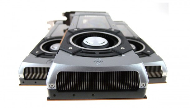 Core clocks on the GK104s drop just a little, though, from a 1006 MHz base down to 915 MHz. Setting a lower guaranteed ceiling is a concession needed to duck in under a 300 W TDP. However, in cases where that power limit isn’t being hit, Nvidia rates GPU Boost up to 1019 MHz—just slightly lower than a GeForce GTX 680’s 1058 MHz spec.
Power is actually an important part of the GeForce GTX 690’s story. Nvidia’s GeForce GTX 590 bore a maximum board power of 365 W. One 75 W slot and two 150 W eight-pin plugs pushed the 590 mighty close to its ceiling. But because the Kepler architecture takes such a profound step forward in efficiency, Nvidia is able to tag its GTX 690 with a 300 W TDP. And yet it still includes two eight-pin inputs able to deliver up to 375 W, including the slot.
Although the GeForce GTX 690’s board-level features are certainly impressive, this story is arguably just as much about the effort Nvidia’s engineers put into building a card that’d operate quietly, more effectively dissipate heat, and look good in the process.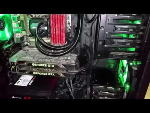 The result is a sturdy, rigid piece of hardware, which demonstrates more showmanship than any reference card preceding it. Back to the preview:
The exterior frame is built of chromium-plated aluminum, rather than the plastic materials covering most other cards (including the GeForce GTX 680). The fan housing itself is a magnesium alloy, which purportedly aids heat dissipation and logically improves vibration dampening compared to plastic shrouds.
Dual vapor chambers cover each of the GPUs, similar to what we’ve seen from both Nvidia and AMD in the past. This time, however, a polycarbonate window over each fin stack allows curious enthusiasts to peer “under the hood.” An LED up top can actually be controlled through a new API Nvidia is making available to partners. So, it might respond to load, getting lighter and darker, as an example.
Currently, I should note, the LED simply lights up when the card is powered on. And here’s where we get to the part sure to turn some folks off…
As with dual-GPU boards from the past, Nvidia is using a center-mounted axial fan, which it claims is optimized for moving air without generating a lot of noise. The trouble with axial fans in this configuration is that they exhaust the heat from one GPU out the rear I/O panel, while the second chip’s thermal energy is jettisoned back into your chassis. Both AMD and Nvidia went the axial route last generation, so we have to surmise that it’s logistically the only approach that makes sense. At least the TDP on GeForce GTX 690 is lower than 590, indicating less maximum heat to dissipate.
Talk to some of the boutique system builders out there and they’ll tell you that shifting from centrifugal to axial-flow fans is akin to the manufacturer dealing with its own product’s thermal output, and then saying, “Here, now you figure out what to do with this.” If we’re to imagine that the most relevant application for GeForce GTX 690 is quad-SLI, you basically have the equivalent of two GeForce GTX 680s dumping hot air into your chassis instead of exhausting out. Finally…
The 690’s rear I/O panel plays host to three dual-link DVI outputs and a mini-DisplayPort connector, accommodating four screens total. A single SLI connector up top links the GeForce GTX 690 to one other card, enabling quad-SLI arrays.
Connecting three displays to two GeForce GTX 680s can be a real pain. Although each board offers four display outputs, there are recommended combinations, depending on whether your screens employ DVI, HDMI, or DisplayPort. With three DVI connectors on GeForce GTX 690, configuration becomes significantly easier.
- 1
Current page:
GeForce GTX 690 4 GB: Hands-Off The Magnesium, Pal!
Next Page Overclocking And Tessellation Performance
Get instant access to breaking news, in-depth reviews and helpful tips.
Contact me with news and offers from other Future brandsReceive email from us on behalf of our trusted partners or sponsors
Chris Angelini is an Editor Emeritus at Tom’s Hardware US. He edits hardware reviews and covers high-profile CPU and GPU launches.
EVGA GeForce GTX 690 review
Skip to main content
When you purchase through links on our site, we may earn an affiliate commission.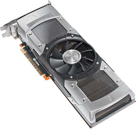 Here’s how it works.
Nvidia’s dual-GPU beauty
TechRadar Verdict
The GTX 690 is a beautifully designed, and wonderfully engineered graphics card. Truly a thing of tech pornography. That said the performance it has on offer isn’t anything wondrous compared to the cheaper GTX 670 SLI alternative.
Why you can trust TechRadar
Our expert reviewers spend hours testing and comparing products and services so you can choose the best for you. Find out more about how we test.
The Nvidia GeForce GTX 690 has been hailed by the green graphics giant as ‘the best graphics card that’s ever been made.’
That’s quite a claim, but bandying around phrases like ‘trivalent chromium plating’ and ‘injection moulded magnesium alloy’ in relation to its design means this expensive ol’ graphics card bears serious inspection.
So yeah, before we get into all the tech pornography that is the Nvidia GTX 690 reference design — here showcased by EVGA — and it’s technological make up, we do need to talk about that £830/$1000 price tag.
That’s a huge amount of money to spend on any PC component, and granted, 90% of us would never even think of dropping that much money on a graphics card. But there are people out there with a penchant for the fastest whatever available and with the means to purchase them.
We’ve already covered the £1,400 Intel Xeon E5-2687W, the absolute pinnacle of CPU performance, and in relation the GTX 690 is actually rather cheap…
Okay, ‘cheap’ might be pushing it a little but you can see where we’re going with this.
As the top fantasy graphics config we’ve been recommending the Nvidia GTX 680 in SLI configuration up to now, and that setup will cost you the same sort of price as a single GTX 690.
While that pairing is still faster there are significant advantages to just opting for a single graphics card – even one sporting two powerful GPUs – over the SLI configuration.
There’s also the fact system integrators will be looking at the Nvidia GeForce GTX 690 with interest.
It will make things are lot easier in fashioning serious dream machines compared to setting up an SLI rig with hardcore cooling.
There has been consternation though about the GTX 680 not necessarily being the top-end Kepler GPU — more like the sort of architecture we were expecting lower down the Kepler tree – and yet still being priced at the top end.
While, as the fastest graphics card around, Nvidia has the right to price it in relation to the AMD competition, others have claimed it still has a responsibility to try and drive hardware adoption in the PC gaming sphere. Pricing the Kepler cards so high means that they are beyond the reach of most gamers.
Whatever the ethics, or the pricing structure of the graphics card market, there is still no getting away from the fact the Nvidia GeForce GTX 690 is one sexy bit of silicon wondrousness.
Vital stats
GPU
— 2x GK104
SMX modules
— 2x 8
CUDA cores
— 2x 1,536
Base clock
— 915MHz
Boost clock
— 1,019MHz
Memory
— 2x 4GB GDDR5
So what is it that makes the Nvidia GeForce GTX 690 ‘the highest quality, most striking video card ever built?’ Well, that’s what Nvidia reckons, so what’s it actually talking about?
Architecturally it’s talking about a hybrid of the GK104 GPU, which powers both the GTX 680 and the Nvidia GTX 670, with two of those graphics chips crammed onto the same single slice of printed circuit board.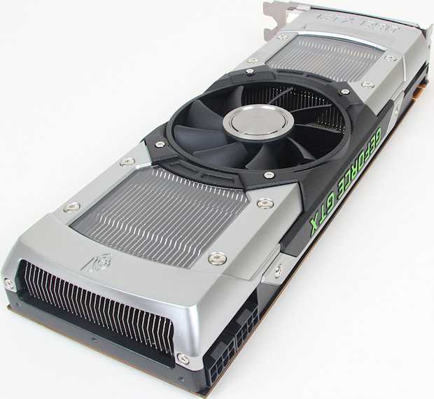
Why a hybrid?
Well, each of the GPUs in this EVGA GeForce GTX 690 contains the same number of CUDA cores that are in the GK104 in the GTX 680. That means we’re looking at a total of 3,072 of those cores in the twin GPUs.
The symmetrical layout ensures each GPU has separate cooling
The two GK104 GPUs aren’t running at GTX 680 speeds though, they are running at 915MHz instead; the same base clock as the new GTX 670 spin of the chip.
We’re also looking at a huge 4GB of GDDR5 (two banks of 2GB) graphics memory sat around the two GPUs. That’s running at the same 6Gbps speed as the memory on the GTX 680.
In order to keep these two chips chock full of juice there’s a 10-phase power setup in between the two chips, with twin 8-pin PCIe power connectors taking the load from the PSU.
That gives the EVGA GTX 690 a relatively conservative 300w TDP. When you think both the previous generation dual-GPU cards — the Nvidia GTX 590 and the AMD Radeon HD 6990 — came with vast power requirements, hitting 365W and 375W respectively, that’s rather efficient.
But the Nvidia GeForce GTX 690 isn’t all about the internal architecture; the actual build of the card screams quality — and expense — from first glance.
The chassis of the card is built from riveted cast aluminium with that trivalent chromium plating. The chrome finish is then highly durable, but is more about aesthetics than anything else.
After all if your graphics card casing needs to be that durable you really need to question what you use it for.
The central fan housing is built from injection moulded magnesium alloy and if that sounds familiar you’re probably a petrol-head as it’s used in the construction of the beautiful Bugatti Veyron’s engine.
Each of the GPUs in turn have their own separate cooling unit, using vapour chamber technology, around a centralised fan. Beneath that fan is a grooved plate to help direct airflow beneath the heat sinks and fins.
The result then is a well-cooled card, that still manages to remain relatively quiet during operation.
- 1
Current page:
Introduction and architecture
Next Page Benchmarks
TechRadar is part of Future US Inc, an international media group and leading digital publisher. Visit our corporate site .
©
Future US, Inc. Full 7th Floor, 130 West 42nd Street,
New York,
NY 10036.
GeForce GTX 690 — Two GPUs Without Compromises / Graphics Cards
A little over a month has passed since the release of the GeForce GTX 680, and now NVIDIA is introducing a card based on the Kepler architecture with two GK104 processors.
You can read a detailed overview of this architecture in the GTX 680 article. In short, Kepler is an upgrade of the Fermi architecture that NVIDIA used in the GeForce 400 and GeForce 500 series. There have been a number of optimizations in the core, but the main change is to increase number of computing units: GK104 has three times as many CUDA cores and twice as many texture modules compared to the GF110 chip (GeForce GTX 580). On the other hand, the GeForce GTX 680 is inferior in some respects to the GTX 580: the memory bus has «narrowed» from 384 to 256 bits, the number of ROPs has decreased from 48 to 32, and streaming multiprocessor schedulers have switched from dynamic scheduling to static scheduling, which significantly reduced performance in non-graphics calculations. nine0003
GK104 is produced according to the 28 nm process technology, and a moderate (compared to that in the Tahiti core from the Radeon HD 7950/7970) number of transistors allowed us to set the base clock frequency of the GPU to 1006 MHz. The memory in the GTX 680 runs at an effective clock speed of 6008 MHz. In addition, NVIDIA has implemented GPU Boost dynamic overclocking technology, which automatically increases the GPU frequency based on power consumption and temperature. In addition to the base clock, the GTX 680 and 690 specifications list Boost Clock, which is the average clock that automatic overclocking reaches in most applications. nine0003
⇡#
Specifications
The GeForce GTX 680 outperforms its main competitor, the Radeon HD 7970, in the aggregate of tests, although the full triumph did not take place. But, just as importantly, the GTX 680 consumes significantly less power and gets by with two six-pin auxiliary power connectors. Obviously, the GK104 should make a good dual-processor video card. The GTX 690 was easier to make than the GTX 590, also for the reason that it is easier to separate two 256-bit memory buses along with chips on one board than two 384-bit ones. In due time to GTX 590 did not explode in a computer, NVIDIA had to make a significant compromise in the specifications. If the GPU and memory in the GTX 580 operate at frequencies of 770 and 4004 MHz, then in the GTX 590 the frequencies are reduced to 607 and 3414 MHz, respectively. Moreover, the GPU voltage control is disabled in the GTX 590. True, some manufacturers have overcome these limitations, and as a result, such monsters as ASUS MARS II with a three-slot cooling system appeared.
This time, the dual-processor card claims to be a complete replacement for two GeForce GTX 680s. Yes, the base frequency of the chips has been reduced from 1006 to 915 MHz, but Boost Clock differs not so much: 1058 and 1019 — the difference is less than four percent. Video memory operates at the same frequency, 6008 MHz. The
GTX 690 consumes much less power than a pair of GeForce GTX 680s: 300W versus 195W x 2. The two eight-pin connectors, together with PCI-E bus power, set the power consumption limit at 375W.
Like the GTX 680, the GTX 690 works with the PCI-E 3.0 bus. And what’s more, it handles it better than the GTX 680. The latter can officially run in PCI-E 3.0 mode only on systems with Ivy Bridge processors, and the most annoying exception was the Sandy Bridge-E platform with the X79 chipset. Without «hacker» manipulations with the registry, the GTX 680 works on it only in PCI-E 2.0 mode. It is not known if this problem will be fixed in the future, but the GTX 690 already supports PCI-E 3.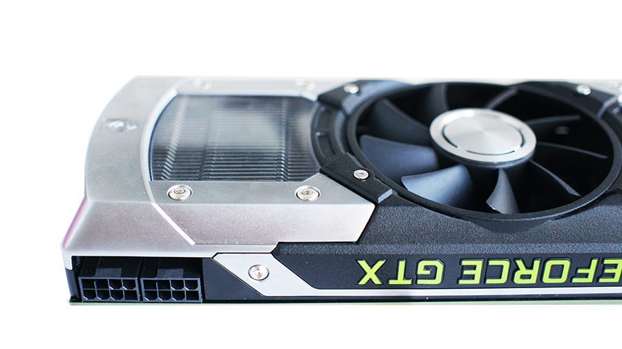 0 on X79 thanks to the PLX PEX8747 bridge, which replaced the NF200 chip that was used in this capacity on the GTX 590 board. It can simultaneously work with PCI-E 2 th and 3rd versions. Regardless of the platform, GPUs always communicate with each other via PCI-E 3.0
The GTX 690 is positioned as the equivalent of two GTX 680s not only in performance but also in price. Suggested retail price is $999 (GTX 680 $499). This is the most expensive reference GeForce in history. Global sales of the GTX 690 have already begun, but it is not yet visible in Russian retail. Which is not surprising: TSMC has not yet started production of the GK104 in sufficient volume, and the vast majority of chips go to the GTX 680. Moreover, NVIDIA will only distribute GTX 690 cards through a few partners. And it is logical to assume that when they penetrate Russia, retailers will raise prices well above the recommended thousand bucks. nine0003
⇡#
Design
The previous two-processor NVIDIA cards differed little in design from the rest of the line. This time, a computer luxury item was made from the flagship model. The casing of the cooling system is almost entirely made of metal. The frame of the cooler is magnesium alloy, the GPU heatsinks are covered with chrome-plated aluminum plates with plexiglass windows. Only narrow plates on the longitudinal edges of the card are plastic. The GTX 690 is one inch longer than the GTX 680 at 11 inches. nine0003
The laser-cut GeForce logo flaunts on the top edge, and even in soft-touch plastic. It glows green in the dark. It is known that NVIDIA does not allow partners to stick branded stickers on the GTX 690 case. It is only allowed to make marks on the printed circuit board.
The design of the cooling system as a whole repeats what we saw on the GeForce GTX 590: GPUs are cooled by two separate heatsinks with a copper evaporation chamber. In the center is a large fan that disperses the air to the sides. As a result, part of the «exhaust» from the video card gets inside the computer case.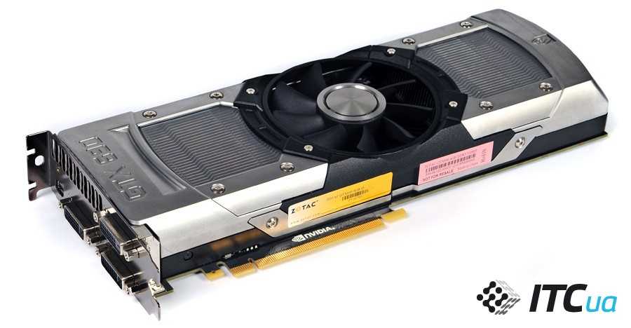 NVIDIA claims that the material of the cooler’s impeller and the angle of the petals are chosen in such a way as to minimize noise. nine0003
The board’s memory chips and batteries are cooled by a massive aluminum frame. Unlike the GTX 590, on the GTX 690 all the attachments fit under the frame, there are no cutouts for tall capacitors. From the fan to the ends of the board there are fins that direct the airflow. There are no plates on the back of the board.
The ports on the rear panel are also slightly different from the GTX 590: one of the DVI outputs is no longer in the middle of the bar, blocking the airflow, but shifted to the side. nine0003
⇡#
Board
The GTX 690 is built on a 10-layer board. All memory chips fit on the front surface.
Like the GeForce GTX 590, the GTX 690 comes with Samsung memory chips (GTX 680 — Hynix). The nominal frequency is the same as that of the GTX 680: 6 GHz, marking — K4G20325FD-FC03.
The board’s power system includes five phases for each GPU. The GTX 680 has only four phases — another unexpected advantage of the GTX 690. The GPU is powered by two ON Semiconductor NCP4206 controllers, which we have not seen before. The memory of each GPU is allocated one phase, controlled by the Anpec APL 3516C controller. All capacitors on the GTX 69 board0 solid-state (GTX 680 also has standard «jars» with liquid electrolyte).
⇡#
Test Method
| Test Stand Configuration | |
|---|---|
| CPU | Intel Core i7-3960X @ 4.6 GHz (100×46) |
| Motherboard | ASUS P9X79 Pro |
| RAM | DDR3 Kingston HyperX 4×2 GB @ 1600 MHz, 9-9-9 |
| ROM | Intel SSD 520 240 GB |
| Power supply | IKONIK Vulcan, 1200W |
| CPU cooler | Thermalright Silver Arrow |
| Housing | CoolerMaster Test Bench V1.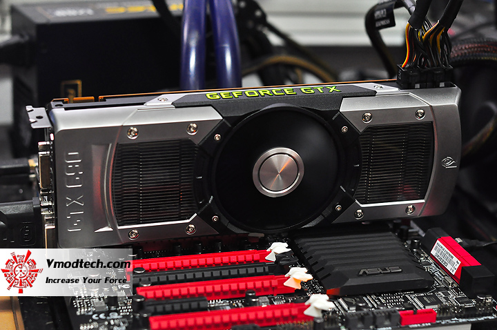 0 0 |
| Operating system | Windows 7 Ultimate X64 Service Pack 1 |
| Software for AMD cards | AMD Catalyst 12.4 + Catalyst Application Profiles 12.4 CAP 1 |
| NVIDIA card software | 301.11 |
| AMD Catalyst Control Center Settings | |
|---|---|
| Antialiasing | Use application settings |
| Anisotropic Filtering | Use application settings |
| Tesselation | Use application settings |
| Catalyst A.I., Texture Filtering Quality | Quality, Enable Surface Format Optimization |
| Mipmap Detail Level | Quality |
| Wait for V-Sync | Off unless application specifies |
| Anti-Aliasing Mode | Multi-sample AA |
| Direct3D Settings, Enable Geomery Instancing | On |
| Triple buffernig | Off |
| NVIDIA Control Panel Settings | |
| Ambient Occlusion | Off |
| Anisotropic Filtering | Application-controlled |
| Antialiasing – Gamma correction | |
| Antialiasing – Mode | Application-controlled |
| Antialiasing – Settings | Application-controlled |
| Antialiasing – Transparency | Off |
| CUDA-GPUs | All |
| Maximum pre-rendered frames | 3 |
| Multi-display/mixed-GPU acceleration | Multiple display performance mode |
| Power management mode | Adaptive |
| Texture filtering – Anisitropic sample optimization | Off |
| Texture filtering – Negative LOD bias | Allow |
| Texture filtering – Quality | Quality |
| Texture filtering – Trilinear optimization | On |
| Threaded optimization | Auto |
| Triple buffering | Off |
| Vertical sync | Use the 3D application settings |
| Program | API | Settings | Test Mode | Resolution 9009 |
|---|---|---|---|---|
| 3DMark 2011 | DirectX 11 | Profiles Performance, Extreme | ||
| Unigine Heaven 2 | DirectX 11 | Max.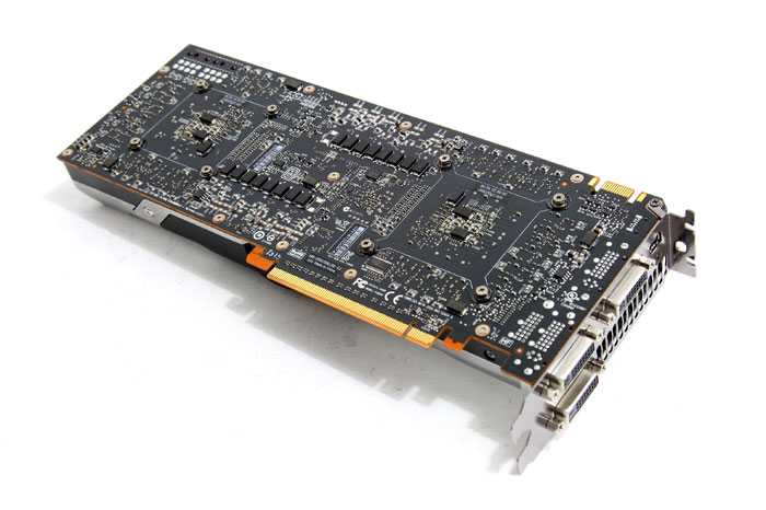 quality, DirectX 11, Extreme mode tessellation quality, DirectX 11, Extreme mode tessellation |
AF 16x, MSAA 4x | 1920×1080 / 2560×1440 |
| Crysis Warhead + Framebuffer Crysis Warhead Benchmarking Tool | DirectX 10 | Frost flythrough. Max. settings, DirectX 10 | AF 16x, MSAA 4x | 1920×1080 / 2560×1440 |
| Metro 2033 + Metro 2033 Benchmark | DirectX 11 | Max. settings, DirectX 11, DOF, tessellation, NVIDIA PhysX off | AF 16x, MSAA 4x | 1920×1080 / 2560×1440 |
| DiRT 3 + Adrenaline Racing Benchmark Tool | DirectX 11 | Aspen, 8 cars. Max. quality, DirectX 11 | AF, AA 4x | 1920×1080 / 2560×1440 |
| Crysis 2 + Adrenaline Crysis 2 Benchmark Tool | DirectX 11 | Central Park. Max. quality, DirectX 11, high resolution textures | AF 16x, Post MSAA + Edge AA | 1920×1080 / 2560×1440 |
| Battlefield 3 + FRAPS | DirectX 11 | Beginning of the Going Hunting mission. Max. quality Max. quality |
AF 16x, MSAA 4x | 1920×1080 / 2560×1440 |
| Batman: Arkham City. Built-in benchmark | DirectX 11 | Max. quality | AF, MSAA 4x | 1920×1080 / 2560×1440 |
| The Elder Scrolls 5: Skyrim + FRAPS | DirectX9 | City of Whiterun. Max. quality | AF 16x, MSAA 4x | 1920×1080 / 2560×1440 |
| Call of Duty: Modern Warfare 3 + FRAPS | DirectX9 | Mission Return to Sender. Max. quality | AF, MSAA 4x | 1920×1080 / 2560×1440 |
The following configurations were tested:
- NVIDIA GeForce GTX 690 (915/6008 MHz, 4 GB)
- 2 x NVIDIA GeForce GTX 680 (1006/6008 MHz, 2 GB)
- 2 x AMD Radeon HD 7970 (925/5500MHz, 3GB)
- NVIDIA GeForce GTX 680 (1006/6008, 2 GB)
- AMD Radeon HD 7970 (925/5500MHz, 3GB)
- NVIDIA GeForce GTX 590 (607/3414MHz, 3GB)
- AMD Radeon HD 6990 (880/5000MHz, 4GB)
⇡#
Overclocking, temperature, power consumption
With the advent of GPU Boost technology, overclocking video cards based on NVIDIA GPUs looks different.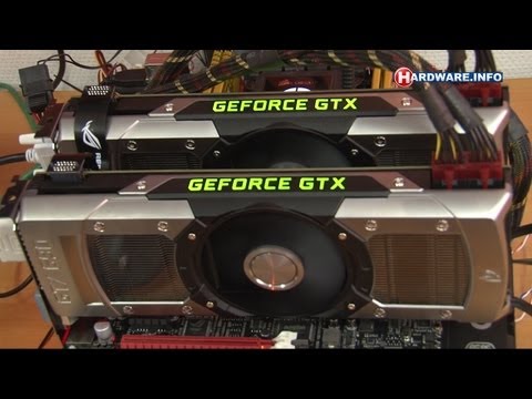 GPU Boost itself performs dynamic overclocking of the processor, increasing the frequency and supply voltage, if there is a reserve for power consumption and temperature. For the GeForce GTX 680, the frequency increases in steps of 13 MHz from 1006 to 1110 MHz (nine states including the base frequency), and the voltage increases from 1.062 to 1.175 V. The video card rarely works at the base frequency even in the most resource-intensive games. So some of the work for the overclocker is already done in advance. nine0010
There are two ways to achieve more. First, you can raise the power limit of the card (Power Target) up to 132%. In this case, GPU Boost will work more aggressively, setting higher operating frequencies under an equal load. Secondly, you can make an increase to the base frequency of the GPU, and then the entire frequency table, according to which the GPU Boost works, will move up by the same megahertz. The supply voltage cannot be manually adjusted. When we tested the GTX 680, we chalked it up to overclocking software, but now it’s clear that NVIDIA just blocked voltage management.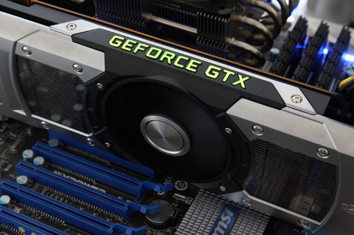 Either it turned out to be incompatible with GPU Boost, or just out of harm’s way. nine0010
Experiments with overclocking the GTX 680 disappointed us somewhat. The base frequency was only increased from 1006 to 1086 MHz. Although at the same time the power reserve of the card and cooling at full speed turned out to be enough for GPU Boost to still use all nine steps of the table, increasing the operating frequency up to 1191 MHz. As a result, the performance gain from overclocking was small.
With GeForce GTX 690 the situation is a bit different. It not only has a larger gap between Base Clock and Boost Clock compared to the GTX 680, but also a longer frequency table — 13 steps, including the initial one. Automatic overclocking can increase the GPU frequency not by 104, but by a maximum of 156 MHz, from 915 to 1071 MHz (but the voltage is greater than 1.175 V anyway). As a result, even in normal mode, the GTX 690 can reach frequencies comparable to those of the GTX 680, while still being able to fall back to a lower base frequency at high power consumption and temperatures.![]() Watching the frequency during the benchmarks showed that in most tasks, the GTX 690 easily reaches the maximum frequencies of 1071 MHz on both GPUs. In particularly difficult tests, one of the processors could retreat a step lower, up to 1058 MHz. nine0003
Watching the frequency during the benchmarks showed that in most tasks, the GTX 690 easily reaches the maximum frequencies of 1071 MHz on both GPUs. In particularly difficult tests, one of the processors could retreat a step lower, up to 1058 MHz. nine0003
The base frequency of the GTX 690 processors was raised to exactly the same level as the GTX 680, 1085 MHz, while maintaining stable operation, which in itself is a great achievement for a «two-headed» card. But the most surprising thing is that GPU Boost still used the top steps of the table, at times increasing the operating frequency of both GPUs as much as 1241 MHz! The GTX 680 only reached 1191 MHz when overclocked.
However, the surprises did not end there. We managed to overclock the memory on the GTX 680 to 1732 (6928) MHz, a little short of the record effective frequency of 7 GHz. But the GTX 690 far surpassed that record: 1902 (7608) MHz! This, apparently, is the merit of Samsung chips.
The GTX 690 has a couple of minor improvements compared to the GTX 680: the ability to increase the power limit by 35% instead of 32%, and the cooler speed — not up to 85, but up to 95%. As a result, the processors of an overclocked card under load heat up 10 ° C less than in normal mode. The fan noise is strong, but tolerable. More interestingly, the operating temperatures of the GTX 680 and GTX 690 are practically the same. Processor Radeon HD 7970 under load has a lower temperature. And both of the previous generation dual-headed cards, the GTX 590 and Radeon HD 6990, run hotter.
In terms of power consumption, the GTX 690 also looks more attractive than the two GTX 680s: the peak power of the systems differs by 15 watts. A pair of Radeon HD 7970s are even more power hungry than the GTX 580 SLI, with a 104W difference compared to the GTX 690! The GTX 590 and HD 6990 are also close to two HD 7970s in terms of power consumption. It is also noteworthy that in 2D mode the GTX 690 consumes no more energy than the GTX 680.
In general, in terms of overclocking and «physics» we are delighted with the GTX 690. The only thing missing, perhaps, is the function to disable the second GPU in idle, as AMD does. In this case, energy consumption could be reduced even more.
GeForce GTX 690 vs. GeForce GTX 680 SLI
The main thing we’re interested in about the performance of the GTX 690 is how it compares to a pair of GTX 680s in an SLI configuration.
3DMark 2011
According to the 3DMark results, there is still a difference in favor of the two GTX 680s.
Gaming tests + Unigine Heaven
And in most gaming tests, the GTX 690 is almost as good as the SLI system. The latter has a noticeable advantage only in DiRT 3. Moreover, the GTX 690 even turned out to be significantly faster in one of the games — Call of Duty: MW3.
Overclocking the GTX 690 has a much greater effect than in the case of the GTX 680. Yes, in CoD: MW3 and Skyrim there is practically no increase in frame rate, but in all other games, the performance increase is often not just big, but colossal. The aggressive work of GPU Boost and incredible memory overclocking showed themselves in all their glory. nine0003
Yes, the frame rate in Crysis 2 is stuck at 100 FPS for all cards, because the game sets such a limit. In this case, we can only say that both configurations provide at least 100 FPS in Crysis 2 even at 2560×1440.
GeForce GTX 690 vs. Radeon HD 7970 CrossFireX, synthetic tests
And now let’s compare the GTX 690 with its main rival — a pair of Radeon HD 7970s in CrossFireX mode, as well as with single-processor cards. Let’s see how well SLI and CrossFireX perform in our benchmarks. nine0003
3DMark 2011
- The GTX 690 in both modes is significantly inferior to the HD 7970 CF in the overall score, but outperforms in the Graphics Score.
- Overclocking the GTX 690 gives it a massive Graphics Score advantage.
- Aside from the GTX 690’s overall score problems, which can be attributed to yet another glitch in 3DMark 2011, both SLI and CF perform well in this test.
Unigine Heaven 2
- Mode 1920×1080 The GTX 690 is noticeably faster than the HD 7970 CF.
- At 2560×1440, the difference between the GTX 690 and HD 7970 CF no longer exceeds a couple of FPS.
- SLI and CF increase performance over single-processor cards with equal success.
The
GeForce GTX 690 vs. Radeon HD 7970 CrossFireX gaming benchmarks
Crysis Warhead (DirectX 10)
- The Radeon HD 7970 pair beats the GTX 690 at both resolutions. This test is memory bandwidth demanding, and the Radeon HD 79’s 384-bit bus70 turned out to be the deciding factor.
- GTX 690 takes revenge when overclocked.
- Both SLI and CF cards offer up to twice the performance of single processor cards.
Metro 2033 (DirectX 11)
- HD 7970 CF wins over GeForce GTX 690.
- Overclocking the GTX 690 only allows you to equalize the points, but not outperform your opponent.
- The increase in performance when using CrossFireX is exactly twofold.
Rare case! SLI doesn’t give that much of a bonus because the GTX 690 and lost.
DiRT 3 (DirectX 11)
- The GTX 690 is noticeably faster than the HD 7970 pair at 2560×1440, but at 1920×1080 the difference is insignificant.
- CrossFireX is slightly more efficient than SLI.
Crysis 2 (DirectX 11)
- Crysis 2 has a 100 FPS limit, so we can only say that both opponents have reached it.
- But if you look at the results of the GTX 680 and Radeon HD 7970 in 2560×1440 mode, you can see that CrossFireX performed more successfully than SLI in this test.
Battlefield 3 (DirectX 11)
- There is no significant difference between the GTX 690 and the HD 7970 CF at 2560×1440, but at 1920×1080 the GTX 690 is still faster.
- Both in the case of SLI and CrossFireX, we have an almost twofold increase in performance compared to single GPUs.
Batman: Arkham City (DirectX 11)
- It’s unfortunate, but in this game CrossFireX not only doesn’t improve performance, but also lowers FPS at 1920×1080.
- The scaling with SLI is far from 100%, but the GeForce GTX 690, of course, still becomes the leader of the test.
The Elder Scrolls 5: Skyrim (DirectX 9)
- GTX 690 is faster than a pair of Radeon HD 7970s.
- Nevertheless, the results of new dual-processor systems, together with the GTX 69 that joined them0 differ little. It looks like Skyrim’s engine just can’t make full use of that kind of processing power. Therefore, the SLI technology allowed the GTX 690 to only pull up the result at a resolution of 2560×1440 by five to six FPS.
- Radeon HD 7970 was initially much slower than the GTX 680, so the effect of CrossFireX was stronger.
The
Call of Duty: Modern Warfare 3 (DirectX 9)
- The GTX 690 vastly outperforms the Radeon HD 7970 CF at both resolutions.
nine0533
- And the SLI technology worked here more effectively than CrossFireX. Even the GTX 590 at 1920×1080 matches the results of the HD 7970 CF.
Conclusions
NVIDIA has indeed made a dual-processor video card that successfully replaces two GeForce GTX 680s. If you need to build an SLI configuration, then there is absolutely no reason to buy separate cards. The GTX 690 is practically on par with the two GTX 680s in terms of performance, and consumes much less energy. But what is most surprising, GTX 69 processors0 also heat up no more than in the GTX 680, while they have exactly the same overclocking potential. Moreover, overclocking the GTX 690 is more efficient because GPU Boost has a higher frequency ceiling. The video memory is completely overclocked to an effective frequency much higher than 7 GHz. What people don’t expect from dual-processor cards is superiority over single-processor cards in overclocking. In addition, for real, so to speak, enthusiasts, it became possible to combine two GTX 690s in a Quad-SLI system. nine0003
A pair of Radeon HD 7970s in CrossFireX mode is a serious competitor to the GeForce GTX 690, but in most of the games we use as benchmarks, either the two configurations are parity or NVIDIA wins. The Radeon HD 7970 has more potential for overclocking and can take revenge in competition with the overclocked GTX 690, but the power consumption of such a system is very high even without overclocking: the bunch of Radeons is much more gluttonous than the GeForce GTX 690. Let’s see if AMD manages to make an equally perfect dual-processor card based on Tahiti chips. nine0003
review and testing of NVIDIA GeForce GTX 690
Contents
- Introduction
- Architectural features, specifications
- NVIDIA GeForce GTX 690
- Packaging and contents, nail puller
- Appearance and dimensions
- Cooling system
- PCB
- Test bench
- Instrumentation and Test Method
- Temperature and noise level
- Performance testing
- Test results
- 3D Mark Vantage
- 3DMark 2011
- Unigine Heaven Benchmark
- Metro 2033
- The Witcher 2: Assassins of Kings
- Battlefield III
- Crysis 2
- S.
T.A.L.K.E.R.: Call of Pripyat
- Lost Planet 2
- Mafia II
- Dragon Age 2
- Hard Reset
- Batman: Arkham City
- F1 2011
- Conclusion
nine0532 Acceleration
Introduction
A few years ago, ATI (already acquired by AMD, but retaining its name for a while, which was later transformed into ATI/AMD, and then completely abolished) developed an extremely effective strategy that allowed it to win back from its eternal competitors from NVIDIA a large share of the market. nine0003
The tactic was simple — make the kernel simpler than the competitor’s, but with good performance, and bring their product line to market as quickly as possible. At the same time, it was supposed to fight the opponent in the upper price segments by increasing frequencies (remember the «overclocked» Radeon HD 4890) and aggressive pricing, and in the top class — by opposing the flagship of the «green» dual-processor video card based on a pair of simple and «non-hot» GPUs .
The calculation was good and fully justified itself. But NVIDIA specialists also did not sit idly by. Radeon HD 3870×2 was promptly answered in the form of GeForce 9800GX2, the competitor of the Radeon HD 4870×2 was the GeForce GTX 295… In each case, NVIDIA developers had to work hard to create a dual-processor accelerator based on voracious GPUs, which were much better suited to work in a single version. A pair of GF100s (GeForce GTX 480/470) could not be combined on one board.
AMD designers had a much easier job. Think about it — not since the days of the Radeon HD 2900 (which is four generations, for the computer industry — an eternity) has a top-end AMD / ATI graphics processor been larger in area, did not contain more transistors, did not have more heat dissipation than a competing NVIDIA solution. Of course, such GPUs are much easier to «glue» into a dual-processor card. nine0003
You can read more about the ups and downs of the struggle between the two vendors in «A Brief History of the Evolution of Dual-GPU Video Cards». Why all this now? In my opinion, the situation is repeated in a «mirror» version. For the first time in a long time, NVIDIA has released a simpler (read, «containing fewer transistors») graphics processor than a competitor.
Interestingly, according to the generally accepted version, NVIDIA’s design department «dreamed» about another «hot monster» — GK100/110, but something did not grow together, and the deadlines were running out, so it was decided to focus on a thorough refinement of the junior GK104 GPU, which (this is clearly hinted at by the digital index) was originally designed for a middle-class card. The end result was even better than expected. nine0003
The GeForce GTX 680, thanks to its progressive architecture and «sharpened» drivers, outperforms the formidable Radeon HD 7970 in most tests, or at least goes on a par with it. At the same time, the card retains a number of features that are typical not for a flagship, but specifically for «middle class» accelerators: small overall dimensions, moderate levels of power consumption and heat dissipation. The relatively simple GPU allowed NVIDIA to pursue an aggressive pricing policy: the GTX 680 was originally announced at $50 less than the Radeon HD 7970.
recommendations
Now success needs to be consolidated. A pair of small GPUs is ideal for creating a «two-headed» flagship. It is this card — the latest GeForce GTX 690 — that is the main character of this article. It’s interesting to see if NVIDIA’s designers managed to create a truly successful product of the highest price category… such that now their colleagues from AMD would have to rack their brains by combining a pair of voracious Tahiti GPUs on one board. nine0003
Architectural features, specifications
First, I’ll give you a table of characteristics, which contains data on all the cards that take part in testing. The exception is the GeForce GTX 580, this accelerator did not participate in the tests, since it belongs to the previous generation and is noticeably inferior to the rest of the participants in terms of performance. However, its characteristics are necessary for comparison with the GTX 590 in order to more clearly describe the «recipe» by which NVIDIA creates its dual-processor solutions. nine0003
|
Name |
HD 7970 |
GTX 580 |
GTX 590 |
GTX 680 |
GTX 690 |
| GPU name |
nine0815 Tahiti XT |
GF110 |
GF110x2 |
GK104 |
GK104x2 |
| Process technology, nm |
28 |
40 |
40 nine0821 |
28 |
28 |
| Core area, mm 2 |
365 |
~530 |
~530×2 |
294 |
294×2 |
| Number of transistors, mln. |
4300 |
3300 |
3300×2 |
3540 |
3540×2 |
| Core frequency, MHz |
925 |
772 / 1544 nine0821 |
608/1216 |
1006 * |
915* |
| Number of shaders (PS), pcs. |
2048 |
512 |
512×2 |
1536 nine0821 |
1536×2 |
| Number of rasterization blocks (ROP), pcs. |
32 |
48 |
48×2 |
32 |
32×2 |
| Number of texture units (TMU), pcs. nine0065 |
128 |
64 |
64×2 |
128 |
128×2 |
| Max. fill speed, Gpix/s |
29.6 |
37.1 |
nine0815 58.4 |
32 |
58. |
| Max. texture fetch rate, Gtex/s |
118.5 |
49.4 |
77.8 |
128 |
234.2 nine0821 |
| Pixel/Vertex shader version |
5.0 / 5.0 |
5.0 / 5.0 |
5.0 / 5.0 |
5.0 / 5.0 |
5.0 / 5.0 |
| Memory type |
GDDR5 nine0821 |
GDDR5 |
GDDR5 |
GDDR5 |
GDDR5 |
| Effective memory frequency, MHz |
5500 |
4008 |
3420 |
6008 |
|
| Memory, MB |
3072 |
1536 |
1536×2 |
2048 |
2048×2 |
| Memory bus width, bit |
384 |
384 |
384×2 |
256 |
256 |
| Memory bandwidth GB/s |
264 |
192. |
192 |
192×2 |
|
| Power consumption (2D/ 3D), W |
3/250 |
nd / 244 |
nd / 365 |
nd / 195 |
|
| Crossfire/Sli |
Yes |
Yes |
Yes ** |
Yes |
Yes ** |
| Dimensions (LxWxH), mm |
270x111x38 |
280x111x38 |
260x111x38 |
280x111x38 |
|
| MSRP |
550 |
499 |
699 |
500 |
999 |
* Base frequency, excluding GPU Boost.
** Quad-SLI version with two dual processor cards only.
So, the new flagship video card uses a pair of Kepler architecture GPUs, their code name is GK104. nine0003
This GPU is already familiar to overclockers and all hardware enthusiasts from the NVIDIA GeForce GTX 680 accelerator. that GK104 was originally created as a mid-range processor, and only later began to be considered as the basis for a «flagship» card). However, thanks to the advanced 28nm process technology, the core area is much smaller — only 294 mm 2 vs. 530 mm 2 (up to 80% difference). The same applies to the power consumption and heat dissipation of the new GPU.
This is important, since NVIDIA once had to work hard to combine two bulky and «gluttonous» GF110s on one board. With the previous «hundredth» GPU, similar in design and underlying the GeForce GTX 480, this «trick» did not work at all — this is why the «400» series did not have a two-processor card, and AMD dominated the upper price segment with the Radeon HD 5970. It was possible to install two 40nm GPUs on one printed circuit board only after the final break-in of the 40nm process technology (by analogy with the CPU, you can call this a new “stepping”) and the introduction of dynamic frequency control technology, which limited the heating of the card and the load on the power circuits in especially difficult conditions.
And yet, the resulting card, the GTX 590, managed to fit into acceptable limits in terms of power consumption and heat dissipation only after a significant reduction in frequencies compared to the single-processor GTX 580. So the GPU was “slowed down” from 772 to 608 MHz (~27%) with simultaneous decrease in supply voltage, video memory — from 4008 to 3420 MHz (~17%). The situation is different with the new video card: the base core frequency is reduced by only 10% compared to the single-processor model — from 1006 to 915 MHz, the memory was not affected at all and in both cases operates at a frequency of 6000 MHz.
At the same time, the new technical process made it possible to fit the card into a thermal package of 300 W, for comparison, the «cut down» GTX 590 in terms of frequencies has a TDP of 365 W (difference ~ 22%). NVIDIA also cites in its press release an «unofficial» figure of 263 W — according to the company, this is the real consumption of the accelerator under «non-extreme» load in the vast majority of tests and games. According to these data, the GTX 690 is slightly superior to the single-processor GTX 580, for which the figure of 244 watts is declared. nine0003
A document circulated among reviewers repeatedly emphasizes that the GTX 690 is an almost equivalent replacement for a pair of GTX 680s in SLI (an entire section is devoted to this). Looking ahead, I will say that there are all grounds for such an assertion. This accelerator, like the younger model, supports the technology of «dynamic» overclocking GPU BOOST, during testing, frequencies of more than 1 GHz were repeatedly observed at the declared «nominal» of 915 MHz. In addition, NVIDIA experts note that the new product should have a good overclocking potential. nine0003
It is important that at the same time the declared TDP level of the GeForce GTX 690 and GTX 680 differs not twice, but only one and a half (to be precise — by 53%, 300 W vs. 195 W)
Otherwise, the press release is not too interesting. It provides several «advertising» graphs comparing performance with a non-proportional scale…
… a number of minor information for reviewers, and a description of proprietary technologies, most of which are either familiar to our readers for a long time (PhysX, 3D Surround), or were described in a recent review of the «related» GeForce GTX 680 (GPU Boost, Adaptive VSync, modes anti-aliasing FXAA, TXAA). nine0003
In the same material, you can get detailed information about the architecture of the GF104 GPU and its differences from previous NVIDIA GPUs.
So, the conclusions of the section:
- The new video card is based on a pair of Kepler architecture GF104 processors and can be described as «GTX 680×2». These cards have the same type and configuration of the video core, memory bus width, type and amount of video memory (for each GPU).
- The power consumption/heat dissipation level of the new video card (compared to the company’s previous dual-processor model) has been reduced from 365W to 300W.
nine0533
- The accelerator is positioned as an equal replacement for the GeForce GTX 680 SLI with several advantages: the use of only one PCIe slot, lower power consumption, lower noise level (most likely, these data were obtained by the manufacturer when installing two GTX 680 «back to back», but they also need to be taken into account).
On paper, the GeForce GTX 690 looks extremely interesting. With performance comparable to the GTX 680 SLI, this card should be the most powerful single video accelerator in history. And the reduction in heat dissipation compared to the GTX 590 can provide quite an acceptable noise level during operation. Time to move on to the outside.
NVIDIA GeForce GTX 690
Packing and bundle, nail puller
Actually, there can be no question of any «packaging and bundle» in relation to this accelerator. NVIDIA does not release video cards for free sale on its own (although there were reports of small batches under this brand for the American market), so we have a pure test specimen intended exclusively for the press and specialists. Therefore, the section received such an unconventional comic name. nine0003
Most likely, many readers are already aware of NVIDIA’s funny promotion — the news about it was published on Overclockers.ru a couple of days ago. However, it is worth mentioning again.
The point is that the accelerator is supplied to reviewers in a hefty wooden box.
Truly wooden: from thick boards knocked down with nails. Most likely, the company sought to «play» on the military theme — it is generally popular with hardware manufacturers. This is evidenced by the inscription on the lid (it is not easy to translate into Russian — something like “Attention, weapons power for games”), moreover, it is in such boxes that weapons and ammunition are transported in the American army (pay attention to the “army” codes on one side). nine0003
But the situation would be quite trivial if it were not for NVIDIA’s claw hammer, which was handed to me along with the box.
Genuine NVIDIA nail puller: branded, steel, over 1kg:
To enhance the humorous effect, it has the inscription «use when attacked by zombies or . ..».
The joke was a success. Only the lazy did not write about the “nail puller against zombies”. Readers of Overclockers.ru also appreciated the humor, there were a lot of jokes in the comments to the news, starting with variations on the theme “play in the box” and up to the magnificent “two-sided” pun “Well, everything is in order: the PEC and firewood for it.” nine0003
However, this reader is slightly mistaken. “Pech” in the box, indeed, was found — “rolled up” in a thick layer of foam rubber …
… but the disk with «firewood» — no, the new ForceWare 301.33 had to be downloaded from the Internet.
In general, it will be interesting if AMD also responds with something like this when releasing its dual-processor flagship.
Appearance and dimensions
But back to more serious things. The appearance of the accelerator is unusual. nine0003
In the official press release, a lot of attention is paid to «exotic industrial design». At the same time, the manufacturer even slightly goes too far in the flamboyance of expressions: “the casing is made of aluminum and protected by trivalent chromium” — in other words, “chrome-plated”.
«The frame of the fan is made of magnesium alloy… magnesium alloy is used in the construction of the Bugatti Veyron and the F-22 fighter.» Thank God, they decided not to use a carbon printed circuit board and a Kevlar casing. nine0003
Nevertheless, the map looks really fresh and unusual. By the way, the key design element is the transparent windows on the casing “covered” with plastic (after the publication of the first photos of the GTX 690, many wondered what kind of “openings” these were), and is also very functional. Through them it is convenient to inspect the radiator to determine if it is time to clean it from accumulated dust.
Single large blade type fan mounted in the center of the booster. Thanks to the «deaf» casing, the card blows heated air through the grille on the rear panel quite well. But no less flow is observed from the reverse side. Unfortunately, this is the only possible layout to ensure even cooling of two GPUs. However, I believe that there are few who want to use the GTX 690 in a cramped, poorly ventilated enclosure. Yes, and «one-sided» blowing is much better than nothing; most «non-reference» cards with fan blades work just fine, blowing air around.
As for the dimensions of the GeForce GTX 690, take a look at the photo:
This is a «sandwich» of NVIDIA’s new flagship and the company’s previous dual-processor accelerator, the GeForce GTX 590. Their dimensions are identical. The height of video cards is standard — 111 mm (according to the dimensions of the rear panel frame), «thickness» — 38 mm (which corresponds to a «two-slot» layout), length — 280 mm. It is customary to pay attention to the latter indicator, since an excessively long accelerator may not be compatible with some case models. nine0003
The GeForce GTX 690 is fine with this — the card is only 5 mm longer than the standard Radeon HD 7970 (275 mm), 10 mm longer than the GeForce GTX 580 (270 mm). It should normally be installed in all «full» format cases and the vast majority of «medium towers» (Midi Tower).
Four video output connectors are soldered on the rear panel of the accelerator. With the current vogue for multi-screen systems, this makes sense.
Please note that NVIDIA prefers the usual DVI connectors — there are three of them at once, and AMD is trying to use more DisplayPort (GTX 690 only one such video output), although the corresponding monitor models are expensive and relatively rare.
Two 8-pin connectors are provided to power the video card. Let me remind you that the same configuration was used on the GeForce GTX 590.
The location of the connectors on the GeForce GTX 690 and GTX 590 is also the same: they are placed «at the tail» of the card and directed upwards in relation to the PCB of the motherboard. Unlike the GTX 680 on this accelerator, the connectors are located in the classic way, and not “two floors”. nine0003
In a system with a GeForce GTX 690 graphics card, NVIDIA recommends using a power supply with at least 650W output power. This is quite a reasonable figure for a powerful gaming PC.
The GeForce GTX 690 leaves a good impression on the outside. Separately, we can note the unusual design and not the longest length of the accelerator, comparable to high-end single-processor models. By the way, don’t you find the card surprisingly similar to the GeForce GTX 590? If one of NVIDIA’s partner companies suddenly releases an accelerator with a casing covered with stickers, these models will turn out to be «twins», hardly distinguishable upon a cursory examination. In further study of the GTX 690, it turned out that in terms of design it has a lot in common with its predecessor model. Take, for example, the cooling system.
Cooling system
NVIDIA designers have carefully worked out the issue of cleaning the heatsink from dust. Usually it is not given due attention, but in vain — more than once I had to disassemble bench-top video cards “to zero” in order to get to the radiator. Everything is much simpler here.
As already mentioned, it is convenient to inspect the radiator through special windows in the casing. The casing itself is attached to the metal frame-base with the help of screws. Yes, there are quite a lot of them (eight, obviously, this is done to make the card more «monolithic»), but it takes only a couple of minutes to disassemble. nine0003
The casing itself is an unremarkable aluminum piece. After removing it, the card appears like this:
Radiator fins have no «bends» at the ends (they are needed so that the air from the fan passes «along» the radiator without being dissipated, here the shroud itself plays this role), so it is enough to take a brush and go over them from above. It’s comfortable.
The design of the cooling system is extremely similar to that installed on the GeForce GTX 590. Compare. nine0003
GeForce GTX 690:
GeForce GTX 590:
There is a similarity in both the general layout (fan in the center, two separate heatsinks serving GPUs) and specific design solutions.
So, the design is still based on a powerful metal frame, to which both radiators and a fan are attached. She is also responsible for removing heat from power switches and video memory chips.
Contact is made through thermal pads (most of them remained on the printed circuit board, I decided not to remove them “forcibly” so as not to complicate the assembly of the card).
In this case, NVIDIA claims to use a special design of «channels» on the frame (they are located directly under the fan impeller and are exposed to direct airflow). These «channels» effectively direct the airflow towards the radiators, and, moreover, they themselves dissipate heat much better than the previously used small pins and protrusions. Excellent detail work. I can also note that it has increased (compared to the same GTX 590) the contact area of the frame with the main CO heatsinks, which should have a beneficial effect on the temperature regime of the VRM and memory chips.
The radiators themselves, as before, consist of aluminum fins soldered onto flat evaporation chambers. The area of the radiators has slightly increased (this is easy to determine even visually, the inner space of the casing is now used more efficiently), in combination with the described aerodynamic improvements, this should give a good effect. The fan impeller diameter is still 80 mm. The number of blades (nine) has not changed, as well as their profile. nine0003
In general, we have before us the already familiar CO design based on two evaporation chambers, which has undergone some “cosmetic” improvements. Well, together they can significantly increase the cooling efficiency. It is also important that the new video card has less heat dissipation compared to the GeForce GTX 590. All this allows us to hope for a significant improvement in the temperature and noise characteristics of NVIDIA’s dual-processor flagship.
Subscribe to our channel in Yandex.