AMD Radeon R9 350 vs AMD Radeon R7 350X OEM
Comparative analysis of AMD Radeon R9 350 and AMD Radeon R7 350X OEM videocards for all known characteristics in the following categories: Essentials, Technical info, Video outputs and ports, Compatibility, dimensions and requirements, API support, Memory, Technologies.
Benchmark videocards performance analysis: Geekbench — OpenCL, GFXBench 4.0 — Car Chase Offscreen (Frames), GFXBench 4.0 — Car Chase Offscreen (Fps), GFXBench 4.0 — Manhattan (Frames), GFXBench 4.0 — Manhattan (Fps), GFXBench 4.0 — T-Rex (Frames), GFXBench 4.0 — T-Rex (Fps).
AMD Radeon R9 350
Buy on Amazon
vs
AMD Radeon R7 350X OEM
Buy on Amazon
Differences
Reasons to consider the AMD Radeon R9 350
- Videocard is newer: launch date 1 month(s) later
- 2x more pipelines: 768 vs 384
- Around 20% better performance in Geekbench — OpenCL: 10504 vs 8761
- Around 24% better performance in GFXBench 4.
0 — Car Chase Offscreen (Frames): 2609 vs 2097
- Around 24% better performance in GFXBench 4.0 — Car Chase Offscreen (Fps): 2609 vs 2097
- Around 25% better performance in GFXBench 4.0 — Manhattan (Frames): 3911 vs 3127
- Around 25% better performance in GFXBench 4.0 — Manhattan (Fps): 3911 vs 3127
- Around 41% better performance in GFXBench 4.0 — T-Rex (Frames): 9664 vs 6862
- Around 41% better performance in GFXBench 4.0 — T-Rex (Fps): 9664 vs 6862
| Launch date | 12 June 2015 vs 5 May 2015 |
| Pipelines | 768 vs 384 |
| Geekbench — OpenCL | 10504 vs 8761 |
| GFXBench 4.0 — Car Chase Offscreen (Frames) | 2609 vs 2097 |
GFXBench 4. 0 — Car Chase Offscreen (Fps) 0 — Car Chase Offscreen (Fps) |
2609 vs 2097 |
| GFXBench 4.0 — Manhattan (Frames) | 3911 vs 3127 |
| GFXBench 4.0 — Manhattan (Fps) | 3911 vs 3127 |
| GFXBench 4.0 — T-Rex (Frames) | 9664 vs 6862 |
| GFXBench 4.0 — T-Rex (Fps) | 9664 vs 6862 |
Reasons to consider the AMD Radeon R7 350X OEM
- Around 8% higher core clock speed: 1000 MHz vs 925 MHz
- Around 46% lower typical power consumption: 65 Watt vs 95 Watt
- 2x more maximum memory size: 4 GB vs 2 GB
- Around 78% higher memory clock speed: 2000 MHz vs 1125 MHz (4500 MHz effective)
| Core clock speed | 1000 MHz vs 925 MHz |
| Thermal Design Power (TDP) | 65 Watt vs 95 Watt |
| Maximum memory size | 4 GB vs 2 GB |
| Memory clock speed | 2000 MHz vs 1125 MHz (4500 MHz effective) |
Compare benchmarks
GPU 1: AMD Radeon R9 350
GPU 2: AMD Radeon R7 350X OEM
| Geekbench — OpenCL |
|
|
||
GFXBench 4. 0 — Car Chase Offscreen (Frames) 0 — Car Chase Offscreen (Frames) |
|
|
||
| GFXBench 4.0 — Car Chase Offscreen (Fps) |
|
|
||
| GFXBench 4.0 — Manhattan (Frames) |
|
|
||
GFXBench 4. 0 — Manhattan (Fps) 0 — Manhattan (Fps) |
|
|
||
| GFXBench 4.0 — T-Rex (Frames) |
|
|
||
| GFXBench 4.0 — T-Rex (Fps) |
|
|
| Name | AMD Radeon R9 350 | AMD Radeon R7 350X OEM |
|---|---|---|
| Geekbench — OpenCL | 10504 | 8761 |
GFXBench 4. 0 — Car Chase Offscreen (Frames) 0 — Car Chase Offscreen (Frames) |
2609 | 2097 |
| GFXBench 4.0 — Car Chase Offscreen (Fps) | 2609 | 2097 |
| GFXBench 4.0 — Manhattan (Frames) | 3911 | 3127 |
| GFXBench 4.0 — Manhattan (Fps) | 3911 | 3127 |
| GFXBench 4.0 — T-Rex (Frames) | 9664 | 6862 |
| GFXBench 4.0 — T-Rex (Fps) | 9664 | 6862 |
Compare specifications (specs)
| AMD Radeon R9 350 | AMD Radeon R7 350X OEM | |
|---|---|---|
| Architecture | Tobago | GCN 1. 0 0 |
| Launch date | 12 June 2015 | 5 May 2015 |
| Place in performance rating | 616 | 817 |
| Type | Desktop | Desktop |
| Code name | Oland | |
| Core clock speed | 925 MHz | 1000 MHz |
| Manufacturing process technology | 28 nm | 28 nm |
| Peak Single Precision (FP32) Performance | 1421 GFLOPS | |
| Pipelines | 768 | 384 |
| Thermal Design Power (TDP) | 95 Watt | 65 Watt |
| Boost clock speed | 1050 MHz | |
| Floating-point performance | 806. 4 gflops 4 gflops |
|
| Texture fill rate | 25.2 GTexel / s | |
| Transistor count | 1,040 million | |
| Display Connectors | 2 x DisplayPort, DVI | 1x DVI, 1x HDMI, 1x VGA |
| DisplayPort support | ||
| Dual-link DVI support | ||
| HDCP | ||
| Number of simultaneous displays | 4 | |
| Interface | PCIe 3. 0 x16 0 x16 |
PCIe 3.0 x8 |
| Supplementary power connectors | None | |
| DirectX | 12 | 12.0 (11_1) |
| OpenGL | 4.3 | 4.5 |
| Maximum RAM amount | 2 GB | 4 GB |
| Memory bandwidth | 72 GB/s | 32 GB / s |
| Memory bus width | 128 bit | 128 Bit |
| Memory clock speed | 1125 MHz (4500 MHz effective) | 2000 MHz |
| Memory type | GDDR5 | DDR3 |
| Unified Video Decoder (UVD) |
AMD Radeon R7 350X OEM Specs
|
|
|
|
|
AMD Radeon R7 350X OEM Specs
Specifications of the AMD Radeon R7 350X OEM graphics card dedicated to the desktop sector, with 384 shading units, its maximum frequency is 1,1GHz The table below makes it possible to observe well the lithography, the number of transistors (if present), the offered cache memory, the quantity of texture mapping units, of render output units, the release date, the GFLOPS performance, the values obtained in the benchmark platforms.
Note: Commissions may be earned from the link above.
This page contains references to products from one or more of our advertisers. We may receive compensation when you click on links to those products. For an explanation of our advertising policy, please visit this page.
Specifications:
| Graphics card | AMD Radeon R7 350X OEM | |||
| Market (main) | Desktop | |||
| Release date | Q2 2015 | |||
| Model number | 215-0837000, Oland XT | |||
| GPU name | Oland | |||
| Architecture | GCN 1.0 | |||
| Generation | Pirate Islands R7 300 | |||
| Lithography | 28 nm | |||
| Transistors | 950. 000.000 000.000 |
|||
| Bus interface | PCIe 3.0 x8 | |||
| GPU base clock | 1,00 GHz | |||
| GPU boost clock | 1,05 GHz | |||
| Memory frequency | 1.000 MHz | |||
| Effective memory speed | 2 GB/s | |||
| Memory size | 4 GB | |||
| Memory type | DDR3 | |||
| Memory bus | 128 Bit | |||
| Memory bandwidth | 32,0 GB/s | |||
| TDP | 65 W | |||
| Suggested PSU | 250W ATX Power Supply | |||
| Multicard technology | — | |||
| Outputs |
1x DVI |
|||
| Cores (compute units, SM, SMX) | 6 | |||
| Shading units | 384 | |||
| TMUs | 24 | |||
| ROPs | 8 | |||
| Cache memory | 256 KB | |||
| Pixel fillrate | 8,4 GPixel/s | |||
| Texture fillrate | 25,2 GTexel/s | |||
| Performance FP32 (float) | 806,4 GFLOPS | |||
| Performance FP64 (double) | 50,4 GFLOPS | |||
| Amazon | ||||
| eBay |
Price: For technical reasons, we cannot currently display a price less than 24 hours, or a real-time price. This is why we prefer for the moment not to show a price. You should refer to the respective online stores for the latest price, as well as availability.
TMUs: texture mapping units. This unit was a physical processor separated from the main graphics processing units. It is able to distort a bitmap image, and also to resize it, to rotate it and to place it as a texture onto a plane of a specific 3D model.
ROPs: render output units. The other name of this unit is raster operations pipeline. This hadware component is taking pixel and texel information, and processing it through vector and matrix operations. The result will be a depth value or a final pixel. It is able to control antialiasing with the merge of several sample into one pixel.
Note: Commissions may be earned from the links above.
Performances :
Performance comparison between this graphics card and those of equivalent power, for this we consider the results generated on benchmark softwares and rendering performances.
Pixel fillrate performance comparison for this graphics card:
| Pixel fillrate performance in GPixels/s | |
|---|---|
|
Intel UHD Graphics 770 |
11,6 |
|
Intel UHD Graphics 730 (Alder Lake) |
11,2 |
|
Intel UHD Graphics 710 |
10,4 |
|
Nvidia GeForce 945A |
9,51 |
|
AMD Radeon R7 350X OEM |
8,4 |
|
AMD Radeon R7 350 OEM |
8,4 |
|
AMD Radeon R5 435 OEM |
8,24 |
|
AMD Radeon R7 435 OEM |
7,36 |
|
AMD Radeon R5 340X OEM |
7,2 |
|
AMD Radeon R5 330 OEM |
6,84 |
Note: Commissions may be earned from the links above. These scores are only an
average of the performances got with these graphics cards, you may get different results.
The term pixel fillrate is refering to the number of pixels that the video card is able to generate every second. This performance is achieved by multiplying the raster output units (ROPs) by the clock frequency of the graphics processor unit (GPU).
Texture fillrate performance comparison for this graphics card:
| Texture fillrate performance in GTexels/s | |
|---|---|
|
Dell Radeon R7 450 4GB |
29,6 |
|
AMD Radeon R7 450 OEM |
29,6 |
|
Nvidia GeForce 945A |
28,54 |
|
AMD Radeon R7 350 |
25,6 |
|
AMD Radeon R7 350X OEM |
25,2 |
|
AMD Radeon R7 350 OEM |
25,2 |
|
Nvidia GeForce GT 1010 |
23,49 |
|
Intel UHD Graphics 770 |
23,2 |
|
AMD Radeon R5 340X OEM |
21,6 |
|
AMD Radeon R5 435 OEM |
20,6 |
Note: Commissions may be earned from the links above. These scores are only an
average of the performances got with these graphics cards, you may get different results.
The term texture fillrate refers to the number of map texture elements (texels) that the GPU is capable of generating per second. This performance is achieved by multiplying the texture mapping units (TMUs) by the clock frequency of the graphics processor unit.
FP32 performance comparison (single precision; float; floating-point 32) for this graphics card:
| FP32 Performance in GFLOPS | |
|---|---|
|
Dell Radeon R7 450 4GB |
947,2 |
|
AMD Radeon R7 450 OEM |
947,2 |
|
Nvidia GeForce 945A |
913,2 |
|
AMD Radeon R7 350 |
819,2 |
|
AMD Radeon R7 350X OEM |
806,4 |
|
AMD Radeon R7 350 OEM |
806,4 |
|
Nvidia GeForce GT 1010 |
751,6 |
|
Intel UHD Graphics 770 |
742,4 |
|
AMD Radeon R5 340X OEM |
691,2 |
|
AMD Radeon R5 435 OEM |
659,2 |
Note: Commissions may be earned from the links above. These scores are only an
average of the performances got with these graphics cards, you may get different results.
Single precision floating point format, also known as FP32, is a computer number format that typically occupies 32 bits in PC memory. This represents a wide dynamic range of numeric values that employs a floating point.
List of comparisons:
AMDAMD RadeonAMD Radeon GraphicsAMD Radeon HDAMD Radeon HD 6000AMD Radeon HD 7000AMD Radeon HD 7800AMD Radeon HD 8000AMD Radeon MobileAMD Radeon ProAMD Radeon Pro MobileAMD Radeon R2AMD Radeon R4AMD Radeon R5AMD Radeon R6AMD Radeon R7AMD Radeon R7 200AMD Radeon R9AMD Radeon R9 200AMD Radeon RXAMD Radeon RX 300AMD Radeon RX 400AMD Radeon RX 500AMD Radeon RX 5000AMD Radeon RX 5000 MobileAMD Radeon RX 6000AMD Radeon RX 6000 MobileAMD Radeon RX 7000AMD Radeon RX VegaAMD Radeon VegaAMD Radeon Vega 11AMD Radeon Vega 3AMD Radeon Vega 6AMD Radeon Vega 8AMD Radeon Vega MobileAppleARMARM MaliARM Mali-400ARM Mali-450ARM Mali-470ARM Mali-G31ARM Mali-G51ARM Mali-G52ARM Mali-G57ARM Mali-G610ARM Mali-G68ARM Mali-G71ARM Mali-G710ARM Mali-G72ARM Mali-G76ARM Mali-G77ARM Mali-G78ARM Mali-T720ARM Mali-T760ARM Mali-T764ARM Mali-T820ARM Mali-T830ARM Mali-T860ARM Mali-T880ASRockAsusAsus GeForce 4000ATIATI Radeon HDATI Radeon HD 3000ATI Radeon HD 4000ATI Radeon HD 5000BFGBroadcomBroadcom VideoCoreColorfulColorful GeForce 4000DellDMPEVGAEVGA GeForce 1000EVGA GeForce 1600EVGA GeForce 2000EVGA GeForce 3000GainwardGainward GeForce 4000GigabyteGigabyte GeForce 4000ImaginationImagination PowerVRImagination PowerVR SGX543Imagination PowerVR SGX544IntelIntel ArcIntel Arctic SoundIntel HD GraphicsIntel Iris GraphicsIntel Iris Plus GraphicsIntel Iris Xe Graphics G7Intel Iris Xe Graphics MobileIntel UHD GraphicsIntel UHD Graphics 610Intel UHD Graphics 620Intel UHD Graphics 630Intel UHD Graphics 730Intel Xe GraphicsLeadtekMicrosoftMicrosoft XboxMSIMSI GeForce 3000MSI GeForce 4000NintendoNvidiaNvidia GeForceNvidia GeForce 1000Nvidia GeForce 1000 MobileNvidia GeForce 1600Nvidia GeForce 1600 MobileNvidia GeForce 2000Nvidia GeForce 2000 MobileNvidia GeForce 3000Nvidia GeForce 3000 MobileNvidia GeForce 400Nvidia GeForce 4000Nvidia GeForce 500Nvidia GeForce 600Nvidia GeForce 600MNvidia GeForce 700Nvidia GeForce 700MNvidia GeForce 800M seriesNvidia GeForce 900Nvidia GeForce 900MNvidia GeForce GTNvidia GeForce GT 1000Nvidia GeForce GTXNvidia GeForce GTX 1000Nvidia GeForce GTX 1000 MobileNvidia GeForce GTX 1600Nvidia GeForce GTX 1600 MobileNvidia GeForce GTX 400Nvidia GeForce GTX 500Nvidia GeForce GTX 600Nvidia GeForce GTX 600 MobileNvidia GeForce GTX 700Nvidia GeForce GTX 700 MobileNvidia GeForce GTX 800 MobileNvidia GeForce GTX 900Nvidia GeForce GTX 900 MobileNvidia GeForce MXNvidia GeForce RTXNvidia GeForce RTX 2000Nvidia GeForce RTX 2000 MobileNvidia GeForce RTX 3000Nvidia GeForce RTX 3000 MobileNvidia GeForce RTX 4000Nvidia GM20BNvidia Quadro seriesNvidia TeslaNvidia VoltaPalitPalit GeForce 4000PNYQualcommQualcomm AdrenoSamsungSaplosSapphireSonySony PlayStationValveVeinedaVivanteXFXYestonZotacZotac GeForce 4000Graphics cards groups
List of benchmarks:
FP32 performance
Equivalence:
AMD Radeon R7 350X OEM Nvidia equivalent
Disclaimer:
When you click on links to various merchants on this site and make a purchase, this can result in this site earning a commission. Affiliate programs and affiliations include, but are not limited to, the eBay Partner Network.
As an Amazon Associate I earn from qualifying purchases.
This page includes affiliate links for which the administrator of GadgetVersus may earn a commission at no extra cost to you should you make a purchase. These links are indicated using the hashtag #ad.
Information:
We do not assume any responsibility for the data displayed on our website. Please use at your own risk. Some or all of this data may be out of date or incomplete, please refer to the technical page on the respective manufacturer’s website to find the latest up-to-date information regarding the specifics of these products.
Radeon R9 Nano vs Radeon R7 350X comparison. Which video card is better?
Home / Video Card Comparison / Which is Better Radeon R9 Nano or Radeon R7 350X?
|
Radeon R9 Nano |
Radeon R7 350X |
|
August, 2015 | 1GHz | 4GB |
May, 2015 | 1GHz | 4GB DDR3 |
|
Edelmark rating |
Edelmark rated |
Benefits
Why is the Radeon R9 Nano better?
| Much wider memory bus | 4.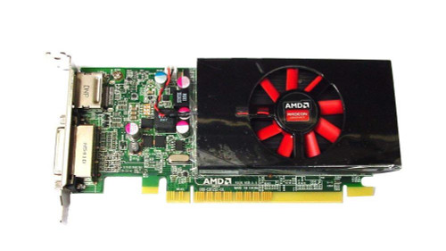 096bit 096bit |
vs | 128bit | 32x wider memory bus |
|---|---|---|---|---|
| Much better floating point performance | 8.192 GFLOPS | vs | 806.4GFLOPS | Approximately 10.2x better floating point performance |
| Much faster texture processing speed | 256 GTexel/s | vs | 25.2 GTexel/s | Approximately 10.2x faster texture rendering speed |
| Many more shaders | 4.096 | vs | 384 | 3712 more shader units |
| Many more texture units | 256 | vs | 24 | 232 more texture units |
| Much faster pixel fill rate | 64 GPixel/s | vs | 8.4GPixel/s | More than 7.5x faster pixel fill rate |
| Many more computing units | 64 | vs | 6 | 58 more computing units |
| Many more raster operation blocks | 64 | vs | 8 | 56 more raster operation blocks |
Why is the Radeon R7 350X better?
| Higher effective memory clock speed | 2. 000 MHz 000 MHz |
vs | 1.000 MHz | 2x effective memory clock speed |
|---|---|---|---|---|
| Significantly higher memory clock speed | 1.000 MHz | vs | 500MHz | 2x higher memory clock speed |
| Significantly lower energy consumption | 65W | vs | 175W | 2.7x lower power consumption |
Key Metrics Test
Pixel Fill Rate
The number of pixels a graphics card can display per second
| Radeon R9 Nano | 64 GPixel/s |
|---|---|
| Radeon R7 350X | 8.4GPixel/s |
Texture Fill Rate
Rate at which the graphics card renders textures
| Radeon R9 Nano | 256 GTexel/s |
|---|---|
| Radeon R7 350X | 25.2 GTexel/s |
Floating Point Operations (FLOPS)
GPU Compute Speed
| Radeon R9 Nano | 8. 192 GFLOPS 192 GFLOPS |
|---|---|
| Radeon R7 350X | 806.4 GFLOPS |
Number of shader units
Shaders — GPU subcomponents that work with three-dimensional graphics
| Radeon R9 Nano | 4.096 |
|---|---|
| Radeon R7 350X | 384 |
Number of texture units (TMUs)
Texture units (TMUs) affect the texture fill rate of a graphics scene
| Radeon R9 Nano | 256 |
|---|---|
| Radeon R7 350X | 24 |
Compute units
Discrete cores within the GPU
| Radeon R9 Nano | 64 |
|---|---|
| Radeon R7 350X | 6 |
Specification (specification)
| Parameter | Radeon R9 Nano | Radeon R7 350X |
|---|---|---|
GPU |
||
| GPU manufacturer | ||
| GPU name | Oland | |
| Platform | Desktop | Desktop |
| Clock frequency | 1. 000 MHz 000 MHz |
1.000 MHz |
| Two | No | No |
| Reference card | No | No |
Rated speed |
||
| Number of shader units | 4.096 | 384 |
| Number of texture units (TMU) | 256 | 24 |
| Number of ROPs | 64 | 8 |
| Computer units | 64 | 6 |
| Pixel fill rate | 64 GPixel/s | 8.4GPixel/s |
| Texture Fill Rate | 256 GTexel/s | 25.2 GTexel/s |
| Number of floating point operations (FLOPS) | 8.192 GFLOPS | 806.4GFLOPS |
Memory |
||
| Memory clock | 500MHz | 1.000 MHz |
| Effective memory frequency | 1. 000 MHz 000 MHz |
2.000 MHz |
| Memory bus width | 4.096bit | 128bit |
| Video memory size | 4.096 MB | 4.096 MB |
Noise and power |
||
| Power consumption | 175W | 65W |
Tags:compare, radeon r7 350x, radeon r9 nano
specs review and gaming performance test
The Radeon R9 350 graphics card was released by AMD, released on 12 June 2015. The graphics card is designed for desktop computers and is based on the Tobago architecture.
Core frequency — 925 MHz. Number of shader processors — 768. Technological process — 28 nm. Power consumption (TDP) — 95 Watt.
Memory type: GDDR5. The maximum memory size is 2 GB. The memory bus width is 128 bit. Memory frequency — 1125 MHz (4500 MHz effective). The memory bandwidth is 72 GB/s.
Benchmarks
| Geekbench OpenCL |
|
|
||||
GFXBench 4. 0 0 Car Chase Offscreen |
|
|
||||
| GFXBench 4.0 Car Chase Offscreen |
|
|
||||
| GFXBench 4.0 Manhattan |
|
|
||||
GFXBench 4. 0 0 Manhattan |
|
|
||||
| GFXBench 4.0 T-Rex |
|
|
||||
| GFXBench 4.0 T-Rex |
|
|
 000 Fps
 | Name | Meaning |
|---|---|
| Geekbench — OpenCL | 10504 |
| GFXBench 4.0 — Car Chase Offscreen | 2609 Frames |
| GFXBench 4.0 — Car Chase Offscreen | 2609.000 Fps |
| GFXBench 4.0 — Manhattan | 3911 Frames |
| GFXBench 4.0 — Manhattan | 3911.000 Fps |
| GFXBench 4.0 — T-Rex | 9664 Frames |
GFXBench 4.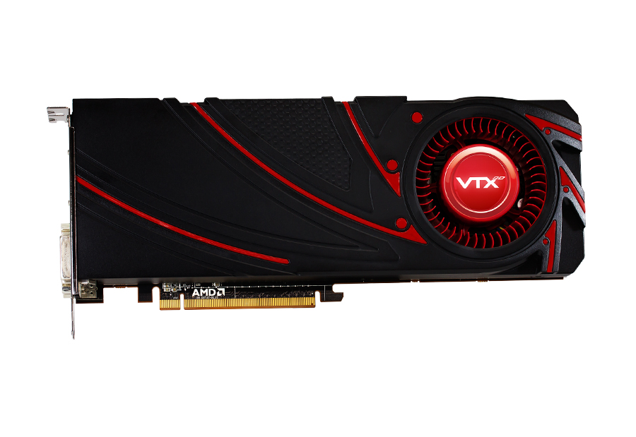 0 — T-Rex 0 — T-Rex |
9664.000 Fps |
Features
| Architecture | Tobago |
| Production date | 12 June 2015 |
| Place in the ranking | 616 |
| Type | Desktop |
| Core frequency | 925MHz |
| Process | 28nm |
| Peak Single Precision (FP32) Performance | 1421 GFLOPS |
| Number of shaders | 768 |
| Power consumption (TDP) | 95 Watt |
| Video connectors | 2 x DisplayPort, DVI |
| DisplayPort support | |
| Dual-link DVI support | |
| HDCP | |
| Number of simultaneous monitors | 4 |
| Interface | PCIe 3.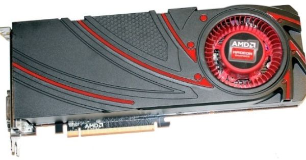
|