How CPUs are made! Explained everything. | by Shubham
CPU is an integral part of all the smart devices we know of such as computers, smartphones, smartwatches, etc. But have you ever wondered how they are made? Probably not, so let’s have a look at how they are made!
1. Sand:
Sand is the basic element or key element from which CPUs are made. But it’s not actually the sand but the silicon in it. Sand consists of 25 percent of silicon. Sand, especially quartz consists of a large amount of silicon in the form of SiO2. So silicon is the basic element from which semiconductors are manufactured.
2. Purifying and melting Silicon:
Ingot
After separating raw sand, and silicon, silicon is purified in multiple steps. After purification, it finally reaches a stage where it is ready for manufacturing the semiconductors. At this stage, the silicon is known as, “Electronic Grade Silicon”. The next phase is melting the Electronic Grade Silicon. After melting the silicon, it is given the shape of a mono-crystal. This mono-crystal is known as “Ingot”. An ingot weighs about 100 kgs and has a silicon of 99.9999%.
3. Ingot slicing and wafer polishing:
Ingot slicing
The ingot is sliced by a very thin and sharp saw into individual disks known as “Wafers” are obtained. There can be various sizes of these wafers depending on the requirements. The general size of the wafers is 300nm. After the wafers are cut, they polished until they have smooth mirror-like surfaces.
4. Photo resist application and UV light exposure:
photo resist applicationUV light eposure
While the wafer is spinning at high speed, a blue photo resist liquid is poured over the wafer. Due to the high spinning of the wafer, a thin and consistent layer is deposited on its surface.
Once the application of photo resist is completed, the wafer is exposed to UV light which performs a chemical reaction. The exposure is done using something called “masks”. These masks act as stencils while there’s a lens between the mask and the wafer.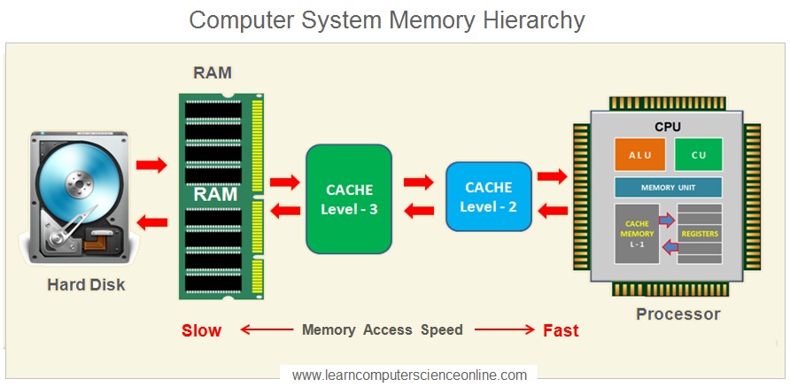 This lens reduces the image of the mask to a small focal point. By this, the size of the lens becomes four times smaller than that of the original one. This procedure is repeated several times in order to achieve a pattern similar to the mask’s pattern. The masks are used create different circuit patterns. The material of the surface of wafers becomes soluble after the exposure.
5. Photo resist washing and etching:
Photo resist washingEtching
The soluble material on the surface is then dissolved and washed with a solvent. This exposes the patterns made the mask. Then, a chemical solvent is used for etching or partially dissolving the substrate part that was exposed. After etching, the photo resist layer is washed away by the similar process, which reveals the desired engraved surface.
6. Ion doping:
ion doping
Before ion doping, the wafers are again applied with photo resist and then washed off again. Then by ion implantation, the exposed areas of the silicon wafer are bombarded with ions. And they change the way that the silicon in these areas conduct the electricity. Once ion implantation is completed, the photo resist is removed and the area of ion doping appears to be green.
After that, three holes are etched on the top insulation layer above the transistor. And these three holes are later filled in with copper to make up the connections of the transistor.
7. Electroplating and layering:
Electroplating and ion doping
The silicon wafers are put into a copper sulphate solution so that only its top is exposed to it. And then on electroplating, copper ions are deposited on the surface of the wafer.
Copper ions settle on the surface of the wafer forming a thin layer of copper. Then the excess material is washed off which leaves a very thin layer of copper. This makes up the whole transistor and after this, these transistors are connected by multiple layers.
Layering
Various transistors are interconnected to each other according to the architecture and design of the particular CPU. This forms a complex circuitry which can have more than 20 layers.
8. Wafer testing & slicing:
Wafer testingWafer slicing
In this step, the wafer is put through a functionality test. In this stage, the wafer is fed through some test patterns and the response is compared to the right answer. These tests determine the good functioning of wafers. Then these wafers are cut into small pieces called “dies”. The good die means the die which gives the right answer passes the test and bad dies are discarded. Passed dies go to the next step which is packaging.
9. CPU testing and packaging:
CPU packaging
In packaging, the substrate (an underlying layer), the die, and the heatspreader are placed together to form a complete processor. On the silver heatspreader, the cooling solution is applied which controls the heat of the processor. After this, there comes a final test where the CPU is tested at its maximum frequency.
It was not until 80386, that the active cooling was required for the CPUs.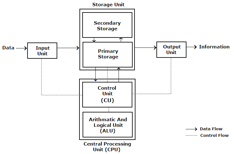 Until then only ceramic top was used because the processors didn’t have enough computing power to generate enough heat. The modern processors generate so much heat that could melt themselves in a few seconds. That is the heatspreader is connected to a larger heatsink (and a fan) so that they work for a longer time.
10. Binning:
CPU binning
Though we can say that the CPU is ready but there is one final step which involves measuring its actual characteristics. Characteristics such as voltages, heat generation, frequency, operational characteristics of caches, etc are measured in binning. Best chips are binned as high-end chips with their full caches enabled. Whereas the chips which do not perform well are sold at their lower clock speeds model or as dual or triple core instead of their quad-core. Others might even have half of their cache disabled (celeron). Here the speeds and voltages are determined. For ex. only 5% of the chips produced might operate at a speed of 3.2GHz while only 50% might operate on 2. 8GHz.
8GHz.
And finally, these tested and manufactured processors are ready to go off to the stores!
This Article Was Originally Published at SpiderPosts.com
From Sand to Processor or How a CPU is made
It is hard to believe that a modern processor (CPU) is the most complex product in the world. What is so complex in this piece of metal?
In this article I will try to explain how a modern processer (CPU) is made from the sand.
Processor Manufacturing
It takes about $ 5 billion dollars to build a processor manufacturing factory. This factory approximately has 4 years to return the invested funds in its technology, before it will start making the profit. If we make some simple calculations that comes to 100 microchips per hour that the factory should manufacture in order to return the invested funds.
The process of processor manufacturing looks like this: the special equipment is used to grow a mono-crystal of cylindrical shape from the molten silicon.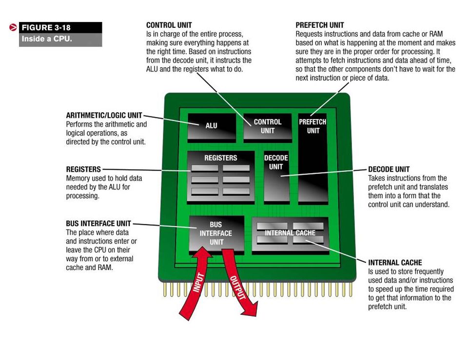 Next, this resulting ingot is cooled and cut into the wafers, which surfaces are carefully leveled and polished to a mirror shine. In the bio-clean rooms of semiconductor factories are created the micro-circuitries on the silicon wafers using photolithography and etching. Then lab personnel make the random testing of processors under a microscope after re-cleaning of the wafers, and if everything is okay, the finished wafers are sliced into individual processors, which later are put in the casing.
Some Chemistry Lessons
Let us take a closer look at the whole process of manufacturing. Sand is made up of 25 percent silicon that is the second most abundant chemical element that’s in the Earth’s crust after oxygen. Sand, especially quartz, has high percentages of silicon in the form of silicon dioxide (SiO2) and is the base ingredient for semiconductor manufacturing.
Originally, it is taken in the form of SiO2 sand, which is in arc furnaces (at the temperature about 1800 ° C) reduced by coke:
SiO2 + 2C = Si + 2CO
This silicon is called a «technical» and has a purity of 98-99.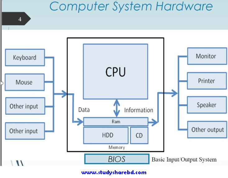 9%. For the manufacturing of processors required pure raw material that is called «electronic grade silicon», which should not have more than one alien atom for every one billion silicon atoms. In order to clean it to such level, silicon literally gets «reborn.» The silicon tetrachloride (SiCl4) is gotten by chlorination of technical silicon, which subsequently is converted into trichlorosilane (SiHCl3):
3SiCl4 + 2h3 + Si ↔ 4SiHCl3
These recycling reactions that are generated by side silicon-contained materials reduce the cost and eliminate the environmental problems:
2SiHCl3 ↔ Sih3Cl2 + SiCl4
2Sih3Cl2 ↔ Sih4Cl + SiHCl3
2Sih4Cl ↔ Sih5 + Sih3Cl2
Sih5 ↔ Si + 2h3
The silicon enters the melting phase after the purification process. In this picture you can see how one big crystal is grown from the purified silicon melt. The resulting mono-crystal is called an ingot. A mono-crystal ingot is produced from electronic grade silicon. One ingot weighs approximately 100 kilograms (or 220 pounds) and has a silicon purity of 99.9999 percent.
The ingot is then moved onto the slicing phase where individual silicon discs, called wafers, are sliced thin. Some ingots can stand higher than five feet. Several different diameters of ingots exist depending on the required wafer size. Today, CPUs are commonly made on 300 mm wafers. Once cut, the wafers are polished until they have flawless, mirror-smooth surfaces. Intel doesn’t produce its own ingots and wafers, and instead purchases manufacturing-ready wafers from third-party companies. Intel’s advanced 45 nm High-K/Metal Gate process uses wafers with a diameter of 300 mm (or 12-inches). When Intel first began making chips, it printed circuits on 50 mm (2-inches) wafers. These days, Intel uses 300 mm wafers, resulting in decreased costs per chip.
Manufacturing of chips contains more than three hundred operations in which more than 20 layers form a complex three-dimensional structure. So, here we will talk very briefly only about the most important stages.
Photolithography
The problem is solved by using photolithography technology. It is the process of transferring geometric shapes on a mask to the surface of a silicon wafer. This process involves many steps such as:
Photo Resist Application
The blue liquid that is depicted below is a photo resist finish similar to those used in a film for photography. The wafer spins during this step to allow an evenly-distributed coating that’s smooth and also very thin.
UV Light Exposure
At this stage, the photo-resistant finish is exposed to ultra violet (UV) light. The chemical reaction triggered by the UV light is similar to what happens to film material in a camera the moment you press the shutter button.
Areas of the resist on the wafer that have been exposed to UV light will become soluble. The exposure is done using masks that act like stencils. When used with UV light, masks create the various circuit patterns. The building of a CPU essentially repeats this process over and over until multiple layers are stacked on top of each other.
A lens (middle) reduces the mask’s image to a small focal point. The resulting “print” on the wafer is typically four times smaller, linearly, than the mask’s pattern.
More Exposing
In the picture we have a representation of what a single transistor would appear like if we could see it with the naked eye. A transistor acts as a switch, controlling the flow of electrical current in a computer chip. Intel researchers have developed transistors so small that they claim roughly 30 million of them could fit on the head of a pin.
Photo Resist Washing
After being exposed to UV light, the exposed blue photo resist areas are completely dissolved by a solvent. This reveals a pattern of photo resist made by the mask. The beginnings of transistors, interconnects, and other electrical contacts begin to grow from this point.
Etching
The photo resist layer protects wafer material that should not be etched away.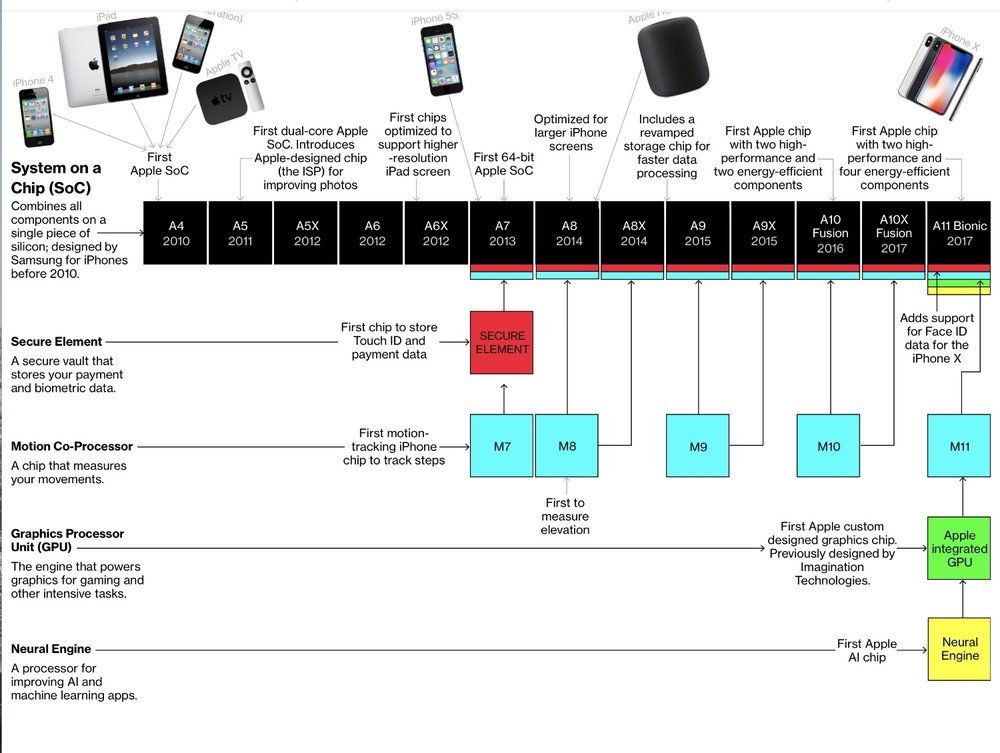 Areas that were exposed will be etched away with chemicals.
Photo Resist Removal
After the etching, the photo resist is removed and the desired shape becomes visible.
Re-applying More Photo Resist
More photo resist (blue) is applied and then re-exposed to UV light. Exposed photo resist is then washed off again before the next step, which is called ion doping. This is the step where ion particles are exposed to the wafer, allowing the silicon to change its chemical properties in a way that allows the CPU to control the flow of electricity.
Ion Doping
Through a process called ion implantation (one form of a process called doping) the exposed areas of the silicon wafer are bombarded with ions. Ions are implanted in the silicon wafer to alter the way silicon in these areas conduct electricity. Ions are propelled onto the surface of the wafer at very high velocities. An electrical field accelerates the ions to a speed of over 185,000 mph.
More Photo Resist Removal
After the ion implantation, the photo resist will be removed and the material that should have been doped (green) now has alien atoms implanted.
A Transistor
This transistor is close to being finished. Three holes have been etched into the insulation layer (magenta color) above the transistor. These three holes will be filled with copper, which will make up the connections to other transistors.
Electroplating the Wafer
The wafers are put into a copper sulphate solution at this stage. Copper ions are deposited onto the transistor through a process called electroplating. The copper ions travel from the positive terminal (anode) to the negative terminal (cathode) which is represented by the wafer.
Ion Setting
The copper ions settle as a thin layer on the wafer surface.
Polishing Excess Material
The excess material is polished off leaving a very thin layer of copper.
Layering
Multiple metal layers are created to interconnects (think wires) in between the various transistors. How these connections have to be “wired” is determined by the architecture and design teams that develop the functionality of the respective processor (for example, Intel’s Core i7 processor). While computer chips look extremely flat, they may actually have over 20 layers to form complex circuitry. If you look at a magnified view of a chip, you will see an intricate network of circuit lines and transistors that look like a futuristic, multi-layered highway system.
Testing
Once all of the metal layers are built up, and the circuits (transistors) are all created, it’s time for testing. A device with lots of prongs sits down on top of the chip, attaching microscopic leads to the chip’s surface. Each lead completes an electrical connection within the chip, simulating how it would operate in final form once packaged into end-consumer products.
A series of test signals are sent to the chip with whatever the results are being read. This level of testing includes not only traditional computational abilities, but also internal diagnostics along with voltage readings, cascade sequences (does data flow through as it should), etc. And however the chip responds as a result of this testing, is what’s stored in a database assigned specifically for that die.
This process is repeated for every die on the entire wafer’s surface while all dies are still on the surface.
Wafer Slicing
After tests determine that the wafer has a good yield of functioning processor units, the wafer is cut into pieces (called dies).
Packaging
At this point, all working dies get put into a physical package. It’s important to note that while they’ve had preliminary tested and were found to operate correctly, this doesn’t mean they’re good CPUs.
The physical packaging process involves placing the silicon die onto a green substrate material, to which tiny gold leads are connected to the chip’s pins or ball grid array, which show through the bottom side of the package. On the top of that, a heat spreader is introduced. This appears as the metal package on top of a chip. When finished, the CPU looks like a traditional package end-consumers buy.
A Finished CPU
A microprocessor is the most complex manufactured product on earth. In fact, it takes hundreds of steps and only the most important ones have been visualized in this picture story.
CPU Binning
Based on the test result of class testing processors with the same capabilities are put into the same transporting trays. This process is called “binning,” a process with which many Tom’s Hardware readers will be familiar. Binning determines the maximum operating frequency of a processor, and batches are divided and sold according to stable specifications.
The best chips are generally binned as higher-end parts, being sold as not only the fastest parts with their full caches enabled, but also the low-voltage and ultra low-voltage models.
Conclusion
Do you own a computer? What is your processor? Computer processor had gone so many complex processes and testing before it is in our home and offices desktop. Compared with first and earlier computer, it is definitely faster, reliable, mobile (like laptop, netbook and tablets), more computing power and run at low power.
These advanced chips and manufacturing are helping to bring together the best of computing, communications, and consumer electronics to enable broader and ever more valuable benefits from technology.
I hope you’ve found this article informative.
Quite a thing, wouldn’t you say?
BONUS
A couple of links from where some phrases were taken:
Intel: Making of a chip
Intel: Sand to Silicon
Tags:
intel, it is interesting, processors, silicon, technology
+4
Papay
4 february 2012, 14:10
7
Add Comment
How Does Sand Become Silicon? CPU Manufacturing Explained
The world runs on information, with humanity creating an estimated 2.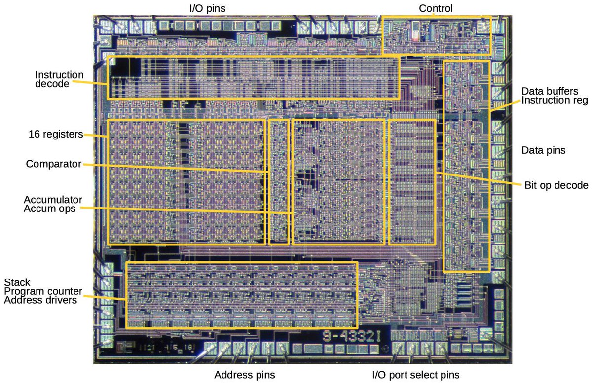 5 million terabytes of data per day. However, all this data is useless unless we can process it, so, arguably, one of the things that the modern world cannot live without is processors.
But how is a processor made? Why is it a modern marvel? How can a manufacturer fit billions of transistors into such a small package? Let’s dive deep into how Intel, one of the largest chip manufacturers globally, creates a CPU from sand.
The base ingredient of any processor, silicon, is extracted from desert sand. This material is found abundantly in the earth’s crust and consists of around 25% to 50% silicon dioxide. It is processed to separate silicon from all other materials in the sand.
The processing repeats several times until the manufacturer creates a 99.9999% pure sample. The purified silicon is then poured to form a cylindrical electronic-grade ingot. The cylinder’s diameter is 300mm and weighs about 100kg.
The manufacturer then slices the ingot into 925-micrometer-thin wafers. Afterward, it’s polished to a mirror-smooth finish, removing all flaws and blemishes on its surface. These finished wafers are then shipped to Intel’s semiconductor fabrication plant for transformation from a slab of silicon into a high-tech computer brain.
The FOUP Highway
As processors are high-precision parts, their pure silicon base mustn’t be contaminated before, during, or after manufacturing. This is where the front-opening unified pods (FOUPs) come in. These automated pods hold 25 wafers at a time, keeping them safe and secure in an environmentally-controlled space when transporting the wafers between machines.
Furthermore, each wafer can travel through the same steps hundreds of times, sometimes going from one end of the building to the other. The entire process is embedded within the machines so that the FOUP knows where to go for each step.
Also, the FOUPs travel on monorails hanging from the ceiling, allowing them to take the fastest, most efficient part from one manufacturing step to another.
Photolithography
Image Source: Chaiken/Wikimedia Commons
The photolithography process uses a photoresist to imprint patterns on the silicon wafer. Photoresist is a tough, light-sensitive material similar to what you find on film. Once this is applied, the wafer is exposed to ultraviolet light with a mask of the processor’s pattern.
The mask ensures that only the places they want to process are exposed, thus leaving the photoresist in that area soluble. Once the pattern is fully imprinted on the silicon wafer, it goes through a chemical bath to remove all the exposed photoresist, leaving a pattern of bare silicon that will go through the next steps in the process.
Ion Implantation
Also known as doping, this process embeds atoms from different elements to improve conductivity. Once complete, the initial photoresist layer is removed, and a new one is put in place to prepare the wafer for the next step.
Etching
After another round of photolithography, the silicon wafer heads on to etching, where the processor’s transistors start to form. Photoresist is applied to areas where they want the silicon to remain, while the parts that must be removed are chemically etched.
The remaining material slowly becomes the transistors’ channels, where the electrons flow from one point to another.
Material Deposition
Once the channels have been created, the silicon wafer returns to photolithography to add or remove photoresist layers as needed. It then proceeds to material deposition. Various layers of different materials, like silicon dioxide, polycrystalline silicon, high-k dielectric, different metal alloys, and copper, are added and etched to create, finalize, and connect the millions of transistors on the chip.
Chemical Mechanical Planarization
Every processor layer undergoes chemical mechanical planarization, also known as polishing, to trim off excess materials. Once the topmost layer is removed, the underlying copper pattern is revealed, allowing the manufacturer to create more copper layers to connect the different transistors as required.
Although processors look impossibly thin, they usually have more than 30 layers of complex circuitry. This allows it to deliver the processing power required by today’s applications.
Testing, Slicing, and Sorting
A silicon wafer can go through all the above processes to create a processor. Once the silicon wafer completes that journey, it then begins testing. This process checks each created piece on the wafer for functionality—whether it works or not.
Once done, the wafer is then cut into pieces called a die. It’s then sorted, where dies that work move forward to packaging, and those that fail are discarded.
Turning the Silicon Die Into a Processor
This process, called packaging, transforms dies into processors. A substrate, typically a printed circuit board, and a heat spreader are put on the die to form the CPU you buy. The substrate is where the die physically connects to the motherboard while the heat spreader interfaces with your CPU’s DC or PWM cooling fan.
Testing and Quality Control
The completed processors are then tested again, but this time for performance, power, and functionality. This test determines what kind of chip it will be—whether it’s good to be an i3, i5, i7, or i9 processor. The processors are then grouped accordingly for retail packaging or placed in trays for delivery to computer manufacturers.
Microscopically Small Yet Immensely Complicated
While processors look simple from the outside, they’re immensely complicated. Processor manufacturing takes two and a half to three months of 24/7 processes. And despite the highly-precise engineering behind these chips, there’s still no guarantee they’ll get a perfect wafer.
In fact, processor makers can lose somewhere between 20% and 70% of the dies on a wafer due to imperfections, contaminants, and more. This value is further impacted by increasingly small CPU processes, with the newest chips going as small as 4nm.
However, as Moore’s Law states, we can still expect processor performance to double every two years until 2025. Until processors hit the fundamental ceiling of atom size, all these manufacturing processes must cope with the designs to produce the chip we demand.
What Is a CPU? Here’s Everything You Need to Know
If you’re just learning about the world of computers and electronics, the terminology used to refer to different parts can be confusing. One component term you may have encountered is “CPU,” which stands for “central processing unit.”
Contents
- What makes a CPU a CPU?
- What does a CPU actually do?
- Cores, clocks, and costs
- How important is the CPU?
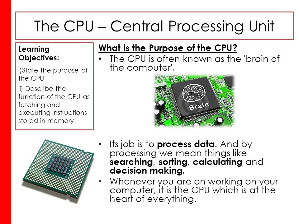
CPUs reside in almost all devices you own, whether it’s a smartwatch, a computer, or a thermostat. They are responsible for processing and executing instructions and act as the brains of your devices. Here, we explain how CPUs interact with other parts of your devices and what makes them so integral to the computing process.
What makes a CPU a CPU?
The CPU is the core component that defines a computing device, and while it is of critical importance, the CPU can only function alongside other hardware. The silicon chip sits in a special socket located on the main circuit board (motherboard or mainboard) inside the device. It is separate from the memory, which is where information is temporarily stored. It is also separate from the graphics card or graphics chip, which renders the video and 3D graphics that are displayed on your screen.
CPUs are built by placing billions of microscopic transistors onto a single computer chip. Those transistors allow it to make the calculations it needs to run programs that are stored on your system’s memory. They’re effectively minute gates that switch on or off, thereby conveying the ones or zeros that translate into everything you do with the device, be it watching videos or writing an email.
One of the most common advancements of CPU technology is in making those transistors smaller and smaller. That’s resulted in the improvement to CPU speed over the decades, often referred to as Moore’s Law.
In the context of modern devices, a desktop or laptop has a dedicated CPU that performs many processing functions for the system. Mobile devices and some tablets instead utilize a System on Chip (SoC) which is a chip that packages the CPU alongside other components. Intel and AMD both offer CPUs with graphics chips and memory stored on them, too, meaning they can do more than just standard CPU functions.
What does a CPU actually do?
At its core, a CPU takes instructions from a program or application and performs a calculation. This process breaks down into three key stages: Fetch, decode, and execute. A CPU fetches the instruction from RAM, decodes what the instruction actually is, and then executes the instruction using relevant parts of the CPU.
The executed instruction, or calculation, can involve basic arithmetic, comparing numbers, performing a function, or moving numbers around in memory. Since everything in a computing device is represented by numbers, you can think of the CPU as a calculator that runs incredibly fast. The resulting workload might start up Windows, display a YouTube video, or calculate compound interest in a spreadsheet.
In modern systems, the CPU acts like the ringmaster at the circus by feeding data to specialized hardware as it is required. For example, the CPU needs to tell the graphics card to show an explosion because you shot a fuel drum or tell the solid-state drive to transfer an Office document to the system’s RAM for quicker access.
Cores, clocks, and costs
Originally, CPUs had a single processing core. Today’s modern CPU consists of multiple cores that allow it to perform multiple instructions at once, effectively cramming several CPUs on a single chip. Most CPUs sold today have two or four cores. Six cores are considered mainstream, while more expensive chips range from eight to a massive 64 cores.
Many processors also employ a technology called multithreading. Imagine a single physical CPU core that can perform two lines of execution (threads) at once, thereby appearing as two “logical” cores on the operating system end. These virtual cores aren’t as powerful as physical cores because they share the same resources, but overall, they can help improve the CPU’s multitasking performance when running compatible software.
Clock speed is prominently advertised when you are looking at CPUs. This is the “gigahertz” (GHz) figure that effectively denotes how many instructions a CPU can handle per second, but that’s not the whole picture regarding performance. Clock speed mostly comes into play when comparing CPUs from the same product family or generation. When all else is the same, a faster clock speed means a faster processor. However, a 3GHz processor from 2010 will deliver less work than a 2GHz processor from 2020.
So, how much should you pay for a CPU? We have several guides to give you some suggestions for the best CPUs you can buy. For a general outline, however, unless you’re a hardcore gamer or someone looking to edit videos, you don’t need to spend more than $250. You can help keep the cost down by avoiding the latest hardware and instead sticking to a recent generation of CPU.
For Intel CPUs, that means 8th-, 9th-, or 10th-generation chips. You can determine their generation by the product name.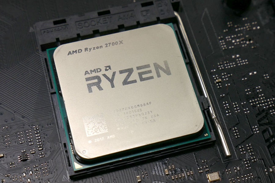 For instance, the Core i7-6820HK is an older 6th-generation chip, while the Core i5-10210U is a newer 10th-generation chip.
AMD does something similar with its Ryzen CPUs: The Ryzen 5 2500X is a 2nd-generation chip based on its new “Zen+” core design, while the Ryzen 9 3950X is a 3rd-generation CPU. Ryzen 4000 was released as a laptop chip line and in APU form with very limited availability on desktop through system builders. With that in mind, it’s arguable whether the Ryzen 5000 is the fourth or fifth generation of AMD Ryzen CPU, but it’s the latest, and most recently, AMD has unified its laptop, APU, and desktop platforms under the Ryzen 5000 banner.
How important is the CPU?
These days, your CPU isn’t as important for overall system performance as it once was, but it still plays a major role in the response and speed of your computing device. Gamers will generally find a benefit from higher clock speeds, while more serious work such as CAD and video editing will see an improvement from a higher CPU core count.
You should bear in mind that your CPU is part of a system, so you want to be sure you have enough RAM and also fast storage that can feed data to your CPU. Perhaps the largest question mark will hang over your graphics card as you generally require some balance within your PC, both in terms of performance and also cost.
Now that you understand the role of a CPU, you are in a better position to make an educated choice about your computing hardware. Use this guide to learn more about the best chips from AMD and Intel.
Editors’ Recommendations
-
Best cheap printer deals for October 2022
-
Best Microsoft Office deals for October 2022
-
The best desktop computers for 2022: Dell, HP, Apple, and more
-
What are mouse jigglers?
-
Best iPad Deals: Latest models on sale from $299
What is CPU (Central Processing Unit)?
Updated: 05/02/2021 by Computer Hope
Alternately referred to as a processor, central processor, or microprocessor, the CPU (pronounced sea-pea-you) is the central processing unit of the computer. A computer’s CPU handles all instructions it receives from hardware and software running on the computer. For example, the CPU processed the instructions to use a web browser to open and display this web page on your computer.
Tip
The CPU is often referred to as the brain of the computer. However, it is more appropriate to refer to software as the brain and the CPU as a very efficient calculator. A CPU is really good with numbers, but if it wasn’t for the software it wouldn’t know how to do anything else.
Note
Many new computer users may improperly call their computer and sometimes their monitor the CPU. When referring to your computer or monitor, it’s proper to refer to them as either the «computer» or «monitor» and not a CPU. The CPU is a chip inside the computer.
- CPU overview
- What does the CPU do?
- CPU history
- Components of the CPU
- Types of CPUs
- How fast does a CPU transfer data?
- Could a GPU be used in place of a CPU?
- Could a computer work without a CPU?
- Related CPU pages.
- CPU help and support.
CPU overview
The picture below is an example of what the bottom and top of an AMD RYZEN processor may look. The processor is placed and secured into a compatible CPU socket found on the motherboard. Processors produce heat, so they are covered with a heat sink to keep them cool and running smoothly. To help transfer the heat between the CPU and the heat sink
As seen in the picture above, the CPU chip is usually square with one notched corner to help make sure it’s properly inserted into the CPU socket. On the bottom of the chip are hundreds of connector pins that correspond to the socket holes. Today, most CPU’s resemble the picture shown above. However, Intel and AMD have also experimented with slot processors. They were much larger and slid into a slot on the motherboard. Also, over the years, there were several types of sockets on motherboards. Each socket only supports specific types of processors and each has its own pin layout.
What does the CPU do?
The CPU’s main function is to take input from a peripheral (keyboard, mouse, printer, etc) or computer program, and interpret what it needs. The CPU then either outputs information to your monitor or performs the peripheral’s requested task.
CPU history
The CPU was first invented and developed at Intel with the help of Ted Hoff and others in the early 1970s. The first processor released by Intel was the 4004 processor, shown in the picture.
- CPU history.
Components of the CPU
In the CPU, there are two primary components.
- ALU (arithmetic logic unit) — performs mathematical, logical, and decision operations.
- CU (control unit) — directs all the processors operations.
Over the history of computer processors, the speed (clock speed) and capabilities of the processor have dramatically improved. For example, the first microprocessor was the Intel 4004 that was released on November 15, 1971, and had 2,300 transistors and performed 60,000 operations per second. The Intel Pentium processor has 3,300,000 transistors and performs around 188,000,000 instructions per second.
Types of CPUs
In the past, computer processors used numbers to identify the processor and help identify faster processors. For example, the Intel 80486 (486) processor is faster than the 80386 (386) processor. After the introduction of the Intel Pentium processor (which would technically be the 80586), all computer processors started using names like Athlon, Duron, Pentium, and Celeron.
Today, in addition to the different names of computer processors, there are different architectures (32-bit and 64-bit), speeds, and capabilities. Below is a list of the more common types of CPUs for home or business computers.
Note
There are multiple versions for some of these CPU types.
AMD processors
| K6-2 K6-III Athlon Duron Athlon XP |
Sempron Athlon 64 Mobile Athlon 64 Athlon XP-M Athlon 64 FX |
Turion 64 Athlon 64 X2 Turion 64 X2 Phenom FX Phenom X4 |
Phenom X3 Athlon 6-series Athlon 4-series Athlon X2 Phenom II |
Athlon II E2 series A4 series A6 series A8 series A10 series |
Intel processors
| 4004 8080 8086 8087 8088 80286 (286) 80386 (386) 80486 (486) |
Pentium Pentium w/ MMX Pentium Pro Pentium II Celeron Pentium III Pentium M Celeron M |
Pentium 4 Mobile Pentium 4-M Pentium D |
Pentium Extreme Edition Core Duo Core 2 Duo |
Core i3 Core i5 Core i7 Core i9 |
The AMD Opteron series and Intel Itanium and Xeon series are CPUs used in servers and high-end workstation computers.
Some mobile devices, like smartphones and tablets, use ARM CPUs. These CPUs are smaller in size, require less power, and generate less heat.
- Full list of computer CPU manufacturers.
How fast does a CPU transfer data?
As with any device that utilizes electrical signals, the data travels very near the speed of light, which is 299,792,458 m/s. How close to the speed of light a signal can get depends on the medium (metal in wire) through which it’s traveling. Most electrical signals are traveling at about 75 to 90% the speed of light.
Could a GPU be used in place of a CPU?
No. Although GPU’s can do many of the same things as a CPU, they lack the ability to perform functions required by some operating systems and software.
Could a computer work without a CPU?
No. All computers require some type of CPU.
- How to determine the type and speed a processor.
- How to install a computer processor.
- CPU help and support.
Computer acronyms, Coprocessor, CPU socket, CPU terms, Dual-core, Hardware terms, Logic chip, Motherboard, Parallel processing, Register
How to squeeze billions of transistors onto a computer chip
Moore’s Law lives on
For decades, the number of tiny transistors studding integrated circuit chips has doubled every two years. That phenomenon — which became known as Moore’s Law — meant faster, more powerful computers. But in recent years the progression has been slowed, some say stopped, by the laws of physics. Increasing the number of circuits on silicon chips, say critics, has reached its limits, and computing will stall at its current level until a substitute approach can be found.
Mukesh Khare disagrees. Khare, who’s responsible for all semiconductor research at IBM, believes the challenges of physics can be overcome. He sees a promising future for adding lots more transistors, the minute engines of computation.
Should we care? Absolutely, says Khare.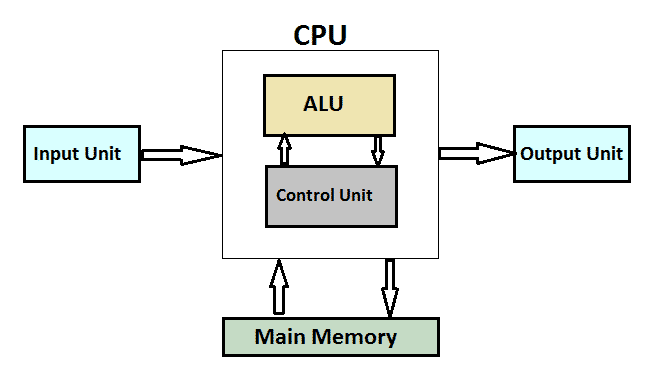 As electronic devices become smaller and more ubiquitous, “putting more transistors on a chip is the way we can continue to bring more value, more functionality, lower cost and lower power consumption,” he explains. And they’re critical for big computer systems as well. “From a systems perspective, we continue to put more and more transistors on a chip so we can have more and more complex functions, integrate them to increase performance of our systems and reduce power.”
How small is 7 nm?
New materials, structures and innovations
So, what about those laws of physics? Well, in the march toward ever-smaller chips, simply shrinking the transistors is not a solution. As they get smaller, they become much harder to imprint on the chips. And their very scale and proximity can affect electrical properties. Signals can “bleed” more easily between them, for example.
“Now it’s all about introducing new materials, new structures, new innovations,” Khare says. “It’s about innovation, not scaling. At a physical level, we still want to make things smaller, but how we do that requires very different concepts and ideas at more fundamental and materials level… it used to be more [about] geometry.”
With that approach, Khare’s team, partnering with GLOBALFOUNDRIES and Samsung at SUNY Polytechnic Institute’s Colleges of Nanoscale Science and Engineering (SUNY Poly CNSE), accomplished that. In July 2015, they unveiled the semiconductor industry’s first 7 nm (nanometer) test chips with functioning transistors. That breakthrough could result in being able to place more than 20 billion transistors on a fingernail-size chip. That’s roughly 10 times as many as are found on today’s chips.
Putting that further into perspective, consider that most of the chips in use today use 22 nm or 14 nm technology. So the new transistors are at least half the current size. And we’re talking really small — 100,000 times smaller than the width of a human hair and about two and half times the circumference of a strand of your DNA.
At the end of the day, it’s the speed at which these structures operate that matters.
Yes it’s small. But does it work?
Going beyond the 7 nm laboratory breakthrough was not without challenges, admits Khare. “One front is being able to build these structures, to be able to etch them and make them physically viable,” he says. “The other part is the electrical aspect. Can these transistors perform? They need to be able to switch on and off and have the proper transistor performance. At the end of the day, it’s the speed at which they operate that matters. Can we increase their speed not only by physical geometry, which is important, but also by changing the materials that we use, or by changing the chemistry we are using to coat and etch these films?”
To answer those questions, the research team came up with some novel processes and techniques. In production, transistors are “printed” on a silicon wafer through a complex process called lithography. To produce the 7 nm chip, the team employed a new type of lithography in the manufacturing process, Extreme Ultraviolet, or EUV, which delivers huge improvements over today’s mainstream optical lithography. And they replaced standard silicon with silicon germanium in the channels on the chips that conduct electricity.
It’s all about introducing new materials, new structures, new innovations.
Learning through fabrication
Khare credits the unique partnership and facilities at CNSE with much of the success. He calls it “a dream come true.” The Albany, NY, research center not only has a 24/7 lab, but also, thanks to tooling partners, the capability of a full-fledged “fab,” a research facility with fabrication capabilities. That’s important because the new chips not only have to be small and efficient, they also have to be economically viable. If it costs too much to produce them, they won’t be successful.
“We can scale to actual tooling, so we can ensure we have the right kind of properties that will scale properly,” says Khare. “We can demonstrate capabilities and structure on realistic fab tools.” Of course, that greatly increases confidence that the chips can be produced economically enough to be commercially successful.
But the collaboration extends beyond the tooling capabilities into all areas of advanced logic technology. “IBM research is leading this effort and we work hand in hand with our other partners, particularly GLOBALFOUNDARIES and Samsung. This is something that one cannot do alone. We have to do it together.”
The next step: researching 5 nm chips
The job is far from over, Khare says, acknowledging, “Seven nanometer still has significant challenges. But research is underway to make even smaller chips. We actually have a have a lot of activity going on beyond 7 nm. This train keeps running.”
“There have been a lot of predictions in the past of the end of semiconductor technology,” he continues. “But with the amount of investment and the number of engineers working on this technology, there’s always a way out; there’s always a path that all these brilliant minds and billions of dollars of investment can find. We are already working on 5 nm technology. That will use many, many additional innovations in both materials and structure. The technology will become harder. It will require more and more new elements and new knowledge.”
And beyond that? He foresees such possibilities as fabricating transistors in three dimensions, stacking circuits atop each other and changing the game by using carbon-based devices. The team is also exploring adding new value to smaller chips such as MRAM or magnetic memory, new ways to interconnect and linking photonics.
“I don’t think this industry is ending,” Khare says. “I think the question is how long will it take to get new chips to the market and at what cost. That is the question.”
Learn more about groundbreaking technology
How the processor works: simple words about the complex
All modern equipment, from wireless headphones to the most complex workstations, runs under the control of a processor. Each of us knows that the processor is the brain of the device, it accepts commands from the user, makes calculations and provides results.
But few understand the intricacies of the work. In this article, we will try to fill this knowledge gap in an accessible way.
Transistors and information coding
You probably know that the first computers occupied entire rooms and even separate buildings. They made calculations using electromechanical relays and vacuum tubes. The revolution took place in the 60s, when the first silicon transistors appeared. Later, integrated monolithic circuits were developed on their basis — prototypes of modern processors.
At the heart of each transistor is a silicon structure. Since silicon is a material with the properties of a semiconductor, depending on the conditions, it can pass an electric current or not. The passed charge is one, the absence of charge is zero. It is with the help of these two values that the binary code is built, with the help of which the computer communicates with the user.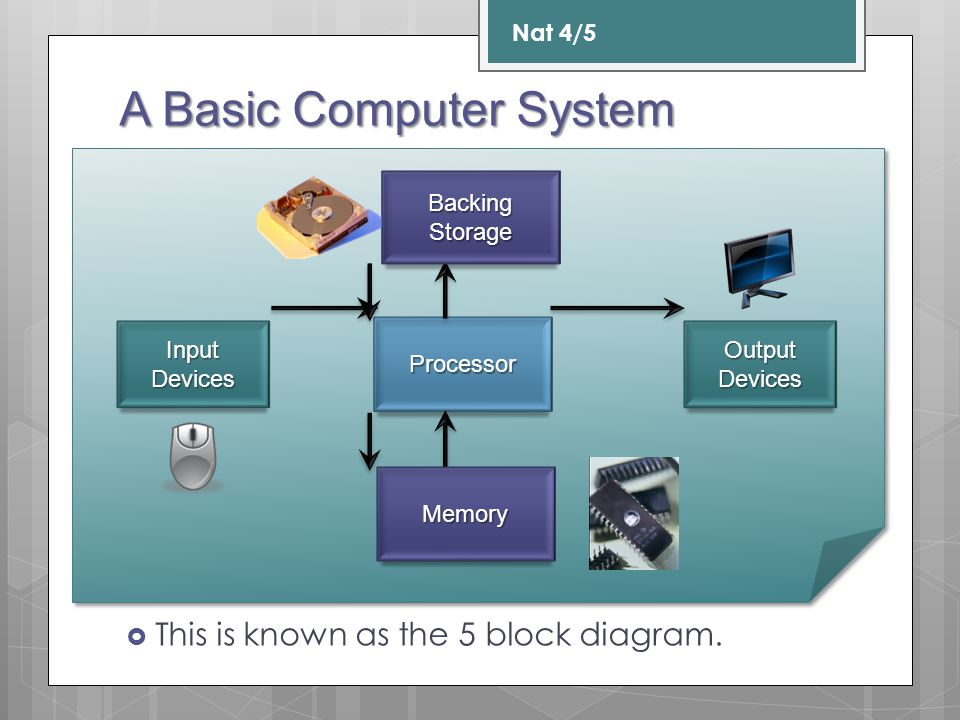 He is unable to receive any other information.
Both 1 and 0 are 1 bit of information, 8 bits make up a byte. Using an 8-digit combination of zeros and ones, you can encode any number from 0 to 255. And with the help of these combinations, assign the appropriate codes to any concepts, meanings and phenomena.
In order for the processor to understand the user, logical forks (operators) were invented. We all know them from the computer science course at school: and / or, if / then / otherwise. Such commands allow the computer to make decisions based on given conditions.
What is a process?
The performance of a processor within one series or family directly depends on the number of transistors: the more transistors, the more combinations are made per unit of time, and the more calculations the device performs.
The first Intel 4004 processor, released in 1971, had 2250 transistors. The Pentium 4 contained 42 million transistors. Modern Epyc processors from AMD are equipped with 39. 54 billion silicon transistors.
The concept of a process technology is closely related to the size of transistors.
The technical process of each of the manufacturers dictates in its own way. Someone is the size of the entire transistor, someone is the size of only one part — the gate. The third option, which will be the most correct, is the step size during production, that is, the minimum size of an element that a developer can operate with when building a circuit. It should also be noted that manufacturers indicate the smallest element, while some electronic elements that cannot be refused can be tens of times larger.
Clock frequency
This concept is often decisive when buying a processor.
Charges passing through the transistors creates a clock generator. The number of pulses per unit time determines the speed of the processor. However, it is not available in every processor. There may be another configuration: the board has one or more clock generators, and they can also be optionally included in microprocessors.
A mandatory element of each processor is a frequency resonator, it gives a correct response to a request in case of serviceability, or does not, which informs the system about a malfunction of the element.
At the heart of each generator there is a quartz crystal. It generates a pulse with a frequency of about 100 MHz. At the moment, oscillators with a frequency of 33 MHz can still be quite common, especially on discrete controllers, such as sound cards, sata / hba adapters and usb / com interface expanders. To increase the frequency, vibrations generated by quartz pass through special nodes — multipliers. They allow you to increase the frequencies at peak loads or reduce them if the load decreases or the computer is idle.
By the way, the multipliers are the very nodes that are responsible for the dynamic increase in the frequency in the load and its decrease in idle time. They can also allow overclocking in the absence of a lock on them to increase beyond the standard value. You can read more about this topic in our article.
For processors with an unlocked multiplier, the user can increase the clock speeds at will. Modern processors can be overclocked by 20 — 30% or even more.
Architecture
The architecture of the processor is the layout of the transistors. Transistors are combined into arrays — cores. Each core in the processor can independently perform various tasks, for this the following cycle of actions is regularly repeated:
- Getting information.
- Decoding.
- Calculation in progress.
- Fixing the result.
Calculations are performed according to special algorithms and instructions that are stored in the temporary memory of the processor.
To increase processor performance, modern computer cores are divided into 2 threads. Each thread is engaged in the execution of separate calculations, providing the processor with multitasking and reducing the task queues.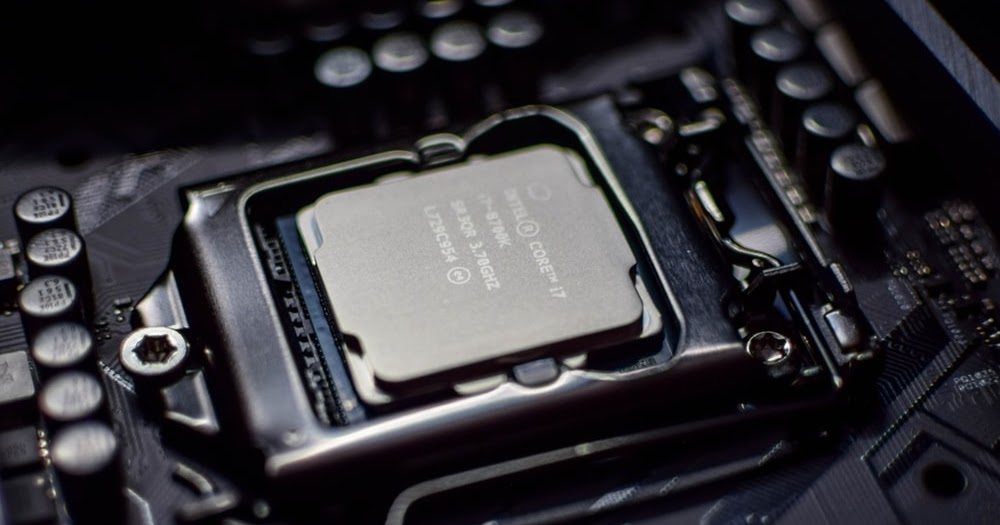
Cache: why does a processor need its own memory?
Hard drives, solid state drives, and RAM aren’t fast enough to meet the demands of the processor. Therefore, each microchip is equipped with its own ultra-fast cache memory that stores data with which the processor is working at a particular moment. The cache also contains instructions for performing specific tasks.
What is a system on a chip?
Modern processors for phones, tablets and laptops have long ceased to be separate computing centers specializing in performing specific tasks. A modern processor is a whole system that includes the actual blocks for performing tasks — the core, as well as a module for rendering images — a graphics adapter. The role of the cores is performed by execution units, which are much larger than in the CPU, and which perform millions of tasks in parallel. Also, some systems may contain additional options, such as a 5G wireless connection center or Thunderbolt data transfer technology.
How does the processor work?
A tool is simpler than a machine. Often the tool is worked by hand, and the machine is driven by steam power or an animal.
Charles Babbage
A computer can also be called a machine, only instead of steam power it uses electricity. But programming has made the computer as simple as any tool.
The processor is the heart/brain of any computer. Its main purpose is arithmetic and logical operations, and before diving into the jungle of the processor, you need to understand its main components and how they work.
The two main components of the processor
Control Unit
The Control Unit (CU) helps the processor control and execute instructions. The CU tells the components exactly what to do. As instructed, it coordinates with other parts of the computer, including the second main component, the arithmetic logic unit (ALU). All instructions first come to the control device.
There are two types of CU implementation:
- Hardwired control units The nature of the work is determined by the internal electrical structure — the device of the printed circuit board or crystal. Accordingly, the modification of such a control unit without physical intervention is impossible.
- microprogrammable control units Can be programmed for certain purposes. The software part is stored in the memory of the CU.
A hard logic CU is faster, but a microprogram controlled CU has more flexible functionality.
Arithmetic logic unit
This unit, oddly enough, performs all arithmetic and logical operations, such as addition, subtraction, logical OR, etc. The ALU consists of logic elements that perform these operations.
Most logic elements have two inputs and one output.
Below is a half adder circuit that has two inputs and two outputs. A and B here are inputs, S is an output, C is a transfer (to the high order).
Arithmetic half-adder circuit
Information storage — registers and memory
As mentioned earlier, the processor executes the commands that come to it. Commands in most cases work with data, which can be intermediate, input or output. All this data, along with instructions, is stored in registers and memory.
Registers
Register is the smallest data memory location. Registers consist of flip-flops (English latches/flip-flops). Triggers, in turn, consist of logical elements and can store 1 bit of information.
Approx. transl. Triggers can be synchronous or asynchronous. Asynchronous can change their state at any time, and synchronous only during a positive / negative edge at the synchronization input.
According to their functionality, triggers are divided into several groups:
- RS-trigger: saves its state at zero levels at both inputs and changes it when it is set to one at one of the inputs (Reset/Set).
- JK-flip-flop: identical to the RS-flip-flop, except that when one is applied to two inputs at once, the flip-flop changes its state to the opposite (counting mode).
- T-flip-flop: changes its state to the opposite with each cycle on its only input.
- D-flip-flop: stores the state of the input at the moment of synchronization. Asynchronous D-flip-flops have no meaning.
RAM is not suitable for storing intermediate data, as this will slow down the processor. Intermediate data is sent to registers on the bus. They can store commands, output data, and even addresses of memory cells.
How the RS flip-flop works
Memory (RAM)
RAM (Random Access Memory, English RAM) is a large group of these same registers connected together. The memory of such a storage is unstable and the data from there disappears when the power is turned off. RAM takes the address of the memory location where the data is to be placed, the data itself, and a write/read flag that activates the triggers.
Approx. transl. RAM is static and dynamic — SRAM and DRAM, respectively. In static memory, cells are flip-flops, and in dynamic memory, capacitors. SRAM is faster and DRAM is cheaper.
Commands (instructions)
Commands are the actual actions that the computer must perform. They are of several types:
- Arithmetic : addition, subtraction, multiplication, etc.
- Logic : AND (logical multiplication/conjunction), OR (logical sum/disjunction), negation, etc.
- Informational :
move,input,outptut,loadandstore. - Jump commands :
goto,if ... goto,callandreturn. - Stop command :
halt.
Approx. transl. In fact, all arithmetic operations in an ALU can be created from just two: addition and shift. However, the more basic operations an ALU supports, the faster it is.
Instructions provided to the computer in assembly language or generated by a high-level language compiler.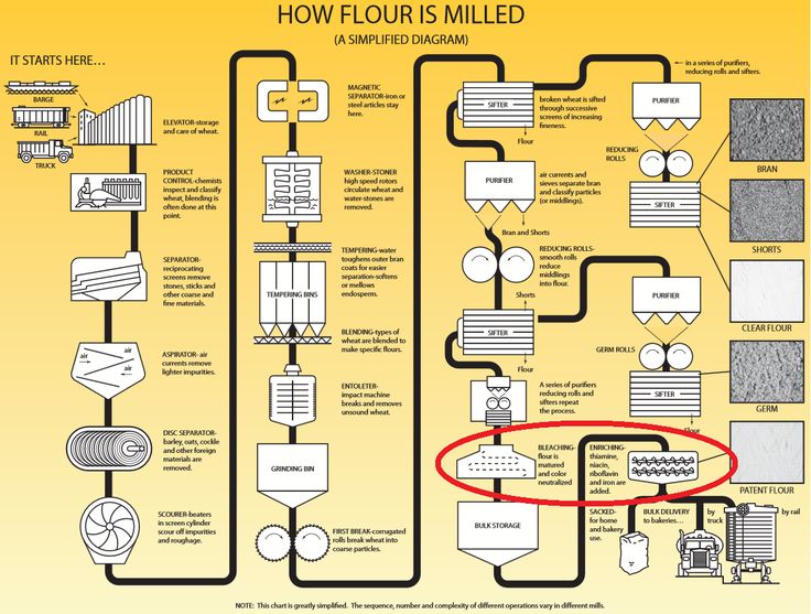
In the processor, instructions are implemented in hardware. In one cycle, a single-core processor can execute one elementary (basic) instruction.
A group of instructions is called an instruction set.
Processor clock
Computer speed is determined by the clock speed of its processor. Clock frequency — the number of cycles (respectively, and executable commands) per second.
The frequency of current processors is measured in GHz (Gigahertz). 1 GHz = 10⁹ Hz is a billion operations per second.
To reduce the execution time of the program, you need to either optimize (reduce) it, or increase the clock frequency. Some processors have the ability to increase the frequency (overclock the processor), however, such actions physically affect the processor and often cause overheating and failure.
Execution of instructions
Instructions are stored in RAM in sequential order. For a hypothetical processor, an instruction consists of an opcode and a memory/register address.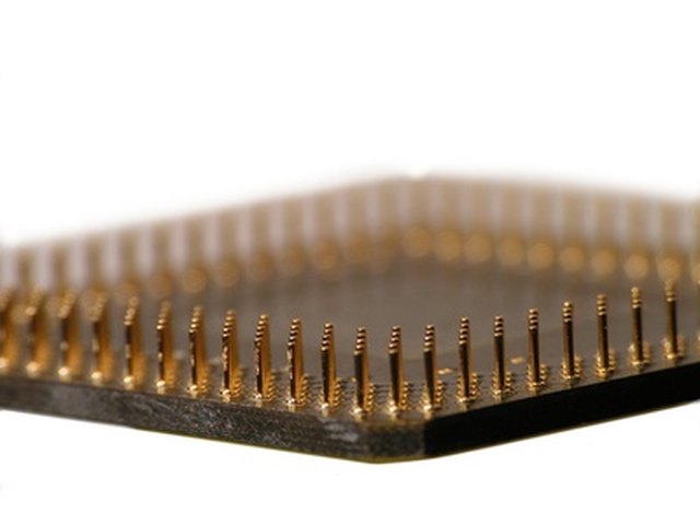 There are two instruction registers inside the control device, into which the instruction code and the address of the currently executing instruction are loaded. The processor also has additional registers that store the last 4 bits of executed instructions.
Below is an example of a set of commands that sums two numbers:
-
LOAD_A 8. This command stores data in RAM, say<1100 1000>. The first 4 bits are the opcode. It is he who defines the instruction. This data is placed in the CU instruction registers. The command is decoded into instructionload_A— put data1000(the last 4 bits of the command) into registerA. -
LOAD_B 2. The situation is similar to the previous one. The number 2 is placed here (0010) to registerB. -
ADD B A. The command adds the two numbers (more precisely, adds the value of registerBto registerA).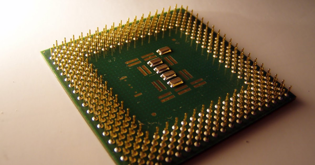 The CU tells the ALU to perform the sum operation and put the result back into register
 A. -
STORE_A 23. We store the value of the registerAin the memory cell with the address23.
These are the operations needed to add two numbers.
Bus
All data between the processor, registers, memory, and I/O devices (input/output devices) is transferred on buses. To load the data just processed into memory, the processor puts the address on the address bus and the data on the data bus. Then you need to give permission to write on the control bus.
Cache
The processor has a mechanism for storing instructions in the cache. As we found out earlier, a processor can execute billions of instructions per second. Therefore, if each instruction were stored in RAM, then its withdrawal from there would take more time than its processing. Therefore, to speed up the work, the processor stores part of the instructions and data in the cache.
If data in cache and memory do not match, they are marked with dirty bits.
Instruction stream
Modern processors can process multiple instructions in parallel. While one instruction is in the decoding stage, the processor can have time to receive another instruction.
However, this solution is only suitable for instructions that are independent of each other.
If the processor is multi-core, this means that it actually has several separate processors with some shared resources, such as cache.
If you want to know more about processors, see what are the popular architectures: CISC, RISC, MISC and others and types.
Translation of the article «How does a CPU work?»
Explain to your child: how does a processor work?
The main element of any computer, laptop, smartphone and other electronic devices is the processor. It is the brain that makes digital cameras take pictures, players play music, animators create new Avatars and Game of Thrones.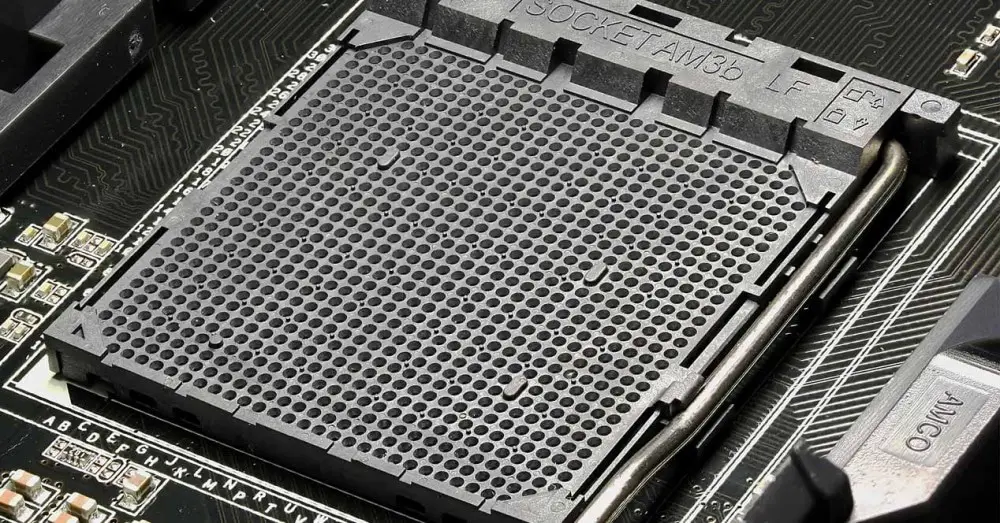 How is this brain? And how does he cope with all these tasks? In today’s article, we will try to deal with these issues.
We will simplify the explanation as much as possible to save you unnecessary details and convey the essence of technology. And we will not even try to explain what exactly happens in the processor when you click on a virtual button in a computer game. If you think about it, today’s missile control systems, smartphones, and millions of other programs and devices exist today precisely because programmers do not have to think about the mechanics of computing processes. It is enough that everything works as it should, and why and how is not important.
From software to microelectronics
This was made possible by the so-called abstraction. Programmers work with virtual objects — this is the highest level of abstraction, which lies at the maximum distance from the machine world and closest to the human world. A little lower is the operating system level, where human-understandable objects are converted into computer processes. You move the mouse — the operating system uses its own mechanisms that are responsible for tracking the cursor and controlling clicks.
If you go even lower, you will deal with the hardware component — RAM, video card, the same processor. These are computer gears whose rotation distributes resources, which in turn power the operating system, which in turn makes applications work. Here, virtual processes move into the technical plane. If you drop acid on the motherboard, it will damage some specific chips, and the function for which the affected elements are responsible will begin to fail in the computer. When you come to a computer wizard and complain that some program freezes for you, he can imagine what material reasons this problem may have — trace its roots through levels of abstraction.
Processor internals
Inside each processor there are two main blocks: a control block (control unit, CU) and a logic block (arithmetic logic unit, ALU). Now we will not dive into the details of their work, the main thing to understand is that when executing computer programs, commands go to the control unit, which understands the instructions, accesses different elements of the computer for the necessary data and transfers them for processing to the logic unit.
The logic block can perform operations with numbers. He returns the result of his work to the control unit, which disposes of them further, in accordance with the conditions of the program he is executing. This separation of duties allows the processor to effectively manage time — one block manages processes, works with memory and other functional elements of the computer, the second solves mathematical problems.
In principle, such a scheme is used in any team work. There is always a leader who deals with organizational issues, communicates with the outside world, obtaining the necessary resources and data, and there are specialists who work with these resources and data, achieving their goals.
CPU work cycle
All work operations inside the processor are organized into a repeating cycle: receive an instruction from memory, read and understand the command, execute it. This endless cycle repeats over and over again as long as your computer is on. A special counter is responsible for its control, which is physically built into the microcircuit — this element, like a conductor, counts the cycles, allowing the processor to clearly perform the necessary work.
This is where the concept of clock frequency came from, which means how many times in one second this conductor will wave his baton. The first stroke — the processor receives an instruction. The second wave — reads and understands the command. The third stroke — performs it. If your computer or smartphone has a processor with a clock speed of 2 GHz (a ridiculous figure in today’s times), two billion strokes occur in it every second. Such fantastic speed of operation allows modern computers to display ultra-clear video with the clearest sound, render three-dimensional spaces in games, and perform many other operations for which we buy computers.
Despite the breadth of possibilities, the set of instructions that the processor works with is rather small. He can read or write data to the specified memory location, perform some operations with them, remember the result, compare it with some number and take one or another action, depending on what turns out to be more. All the magic happens because these operations can be carried out indefinitely and very quickly, fulfilling the conditions of the algorithms that programmers write.
On such, in general, simple principles, the brain of your computer works, in practice proving the ancient wisdom: patience and work will grind everything.
How does a processor work and what is important to know?
The processor is the heart of any computer. We know what it looks like from the outside. But I wonder what it looks like from the inside?
Intel® Core™ i7-1065G7, Ice Lake (10th Gen), 10nm manufacturing process
The processor consists of billions of transistors comparable in size to a DNA molecule. Indeed, the size of a DNA molecule is 10 nm. And this is not some kind of fantasy! Every day, processors help us solve everyday tasks. But have you ever wondered how they do it? And how did people get a piece of silicon to do the calculations for them?
Today we will analyze the basic elements of the processor and in practice we will check what they are responsible for. A handsome laptop — Acer Swift 7 with an Intel processor on board will help us with this.
Processor core
Our processor model is i7-1065G7. It is quad-core and the cores are very clearly visible in the photo.
Each processor core contains all the necessary elements for computing. The more cores, the more parallel computations the processor can perform. This is useful for multitasking and some resource intensive tasks like 3D rendering.
For example, for the test, we launched four 4K videos at the same time. The load on the cores is more or less evenly distributed: we loaded the processor by 68%. As a result, most of all I had to worry about whether the Internet channel would be enough. Modern processors are great at multitasking.
Why is this important? To answer this question, let’s figure it out — how does the kernel work?
At its core, the kernel is a huge data transformation pipeline. At the input we load one, at the output we get another. It is based on transistors. These are miniature switches that can be in just two states: pass current or not. The computer interprets these states as zeros and ones, so all data in the computer is stored in binary code.
We can say that the components inside the computer communicate with each other using a kind of Morse code, which is also an example of a binary code. Only the computer taps us not dots and dashes, but zeros and ones. It would seem that there is some kind of switch, and what can be done with it? It turns out a lot!
If you cleverly connect several transistors together, you can create logic gates. These are the analog equivalents of the “if then” function, like in Excel. If current flows through both wires at the input, then the output will also flow or not, or vice versa, there are not so many options — only seven pieces.
But further combining the gates with each other into complex analog circuits, we force the processor to do different transformations: add, multiply, compare, and so on.
Therefore, the processor core consists of many very complex blocks, each of which can do something different with your data.
Just like a large multi-machine plant, we load raw materials into it — our data. Then we distribute everything among the machines and at the output we get the result.
But how does the processor know what to do with the data? To do this, in addition to the data, we must download the instructions. These are the commands that tell the processor:
- this must be added,
- is multiply,
- is just to send somewhere.
There are a lot of instructions and they are different for each type of processor. For example, mobile processors use a simpler reduced instruction set RISC — reduced instruction set computer.
And in the PC, the instructions are more complicated: CISC — complex instruction set computer.
Therefore, programs from mobile phones do not run on computers and vice versa, processors simply do not understand their commands. But in order to get a result from the processor, it is not enough to say — here is the data for you, do this and that. First of all, it is necessary to say where to get this data from and where, in fact, then to give it. Therefore, in addition to data and instructions, addresses are loaded into the processor.
Memory
To execute a command, the kernel needs at least two addresses: where to get the source data and where to put it.
All the necessary information, i.e. data, instructions and addresses, the processor takes from the main memory. The RAM is very fast, but modern processors are faster. Therefore, to reduce downtime, there is always a cache memory inside the processor. In the photo, the cache is green blocks. As a rule, they put a cache of three levels, and in rare cases four.
The fastest memory is the first level cache, referred to as L1 cache. Usually it is only a few tens of kilobytes. Next comes the L2 cache, it can already be 0.5-1 mb. And the cache of the third level can reach the size of several megabytes.
The rule is simple. The more cache, the less the processor will access RAM, which means less idle.
Our cache processor has as much as 8 MB, which is not bad.
I think everything is clear here, let’s move on.
Clock speed
If the data in the processor came randomly, it would be easy to get confused. Therefore, each processor has its own conductor, which is called a clock generator. It delivers electrical impulses at a certain frequency, which is called the clock frequency.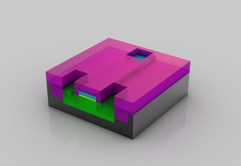 As you understand, the higher the clock frequency, the faster the processor runs.
Interesting fact. In English, clock speed is clock speed. This is a literal term. Computers have a real quartz crystal that vibrates at a certain frequency. Just like in a quartz wrist watch, the crystal counts the seconds, so in computers, the crystal counts the cycles.
Usually the crystal frequency is somewhere around 100 MHz, but modern processors work much faster, so the signal passes through special multipliers. And so the final frequency is obtained.
Modern processors can vary the frequency depending on the complexity of the task. For example, if we are not doing anything and our processor is running at 1.3 GHz, this is called the base frequency. But, for example, if we archive a folder and we see how the frequency immediately increases. The processor goes into turbo mode, and can accelerate up to 3.9 GHz. This approach allows you to save energy when the processor is idle and once again not to heat up.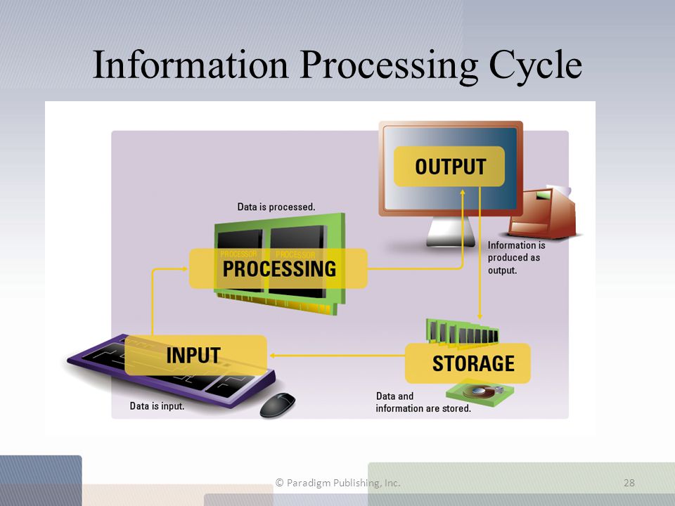
And thanks to Intel Hyper-threading technology, each core is divided into two logical ones and we get 8 independent data streams that a computer can process at the same time.
What’s cool, in the new Intel processors, the speed of frequencies is regulated by a neural network. This allows you to keep the turbo frequencies longer with the same power consumption.
Computing pipeline
Since the processor core is a pipeline, all operations go through standard stages. There are only four of them and they are very simple. In English they are called: Fetch, Decode, Execute, Write-back.
- Fetch
- Decode — decoding
- Execute
- Write-back — write result
First, the task is loaded, then it is decoded, then it is executed, and finally, the result is written somewhere.
The more instructions that can be loaded into the pipeline and the less it is idle, the faster the computer will eventually run.
Transition predictor
To keep the conveyor running, the engineers came up with a lot of tricks. For example, such a thing as a transition predictor. This is a special algorithm that, without waiting for the processor to receive the next instruction, predicts it. That is, it is such a small built-in oracle. You just gave some task, and it is already done.
This mechanism allows you to speed up the system many times over in a lot of scenarios. But the price of an error is high, so engineers are constantly optimizing this algorithm.
Microarchitecture
All the components of the kernel, how everything is organized there, all this is called microarchitecture. The better the microarchitecture is designed, the more efficient the pipeline is. And the more instructions per cycle the processor can execute. This indicator is called IPC — Instruction per Cycle.
This means that if two processors run at the same clock speed, the processor with the higher IPC will win.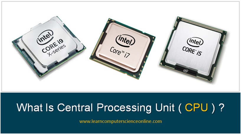
In Ice Lake processors, Intel uses the new architecture for the first time since 2015. It’s called Sunny Cove.
IPC in the new architecture is already 18% higher than in the previous one. This is a big jump. Therefore, when choosing a processor, pay attention to the generation.
System on a chip
Naturally, modern processors are not only the central processing unit. These are entire systems on a chip with many different modules.
GPU
In the new Intel, the GPU takes up the most space. It works on the same principles as the central processing unit. It also has cores, a cache, it also executes instructions. But unlike the central processor, it is sharpened for only one task: to draw pixels on the screen.
Therefore, the cores in graphic processors are much simpler. Therefore, they are even called not cores, but execution units. The more execution units, the better.
In the tenth generation, there are several types of graphics from G1 to G7. This is indicated in the name of the processor.
And there are from 32 to 64 execution units. In the last generation, the most productive graphics were with only 24 units.
The speed of the RAM is also very important for graphics. Therefore, the new Intel brought support for high-speed DDR4 memory with a frequency of 3200 and LPDDR4 with a frequency of 3733 MHz.
We reviewed a laptop with the top-end G7 graphics. So let’s see what she can do! We tested it in games: CS:GO, Dota 2 and Doom Eternal.
What’s convenient — Intel made a gameplay.intel.com portal, where you can find the optimal settings for most games by processor model.
In general, in Full HD resolution, you can comfortably play most games right on the integrated graphics.
Thunderbolt
But there is a cherry on the cake in this processor — this is the Thunderbolt interface. The interface controller is located right on the main chip, right here.
This solution allows not only to save space on the motherboard, but also to significantly reduce delays. Let’s check it out in practice.
Connect an external video card and monitor via Thunderbolt. And let’s run the same games. Now we have a laptop performance level comparable to a powerful gaming PC.
But the Thunderbolt fun doesn’t end there. For example, we can connect an SSD drive to a monitor. And with just one connector on the laptop, we get a powerful computer for games, editing, and in general any resource-intensive tasks.
We have launched the Crystalmark test. You see the results yourself.
But the benefits of Thunderbolt don’t stop there. Through this interface, we can connect an eGPU, a monitor, and the same SSD, and all this through one cable connected to the computer.
I hope we have helped you better understand how the processor works and what its components are responsible for.
Post Views:
9259
How does the processor work inside many types of devices?
The main components inside the processor, the principle of operation, methods of controlling any device with a CPU.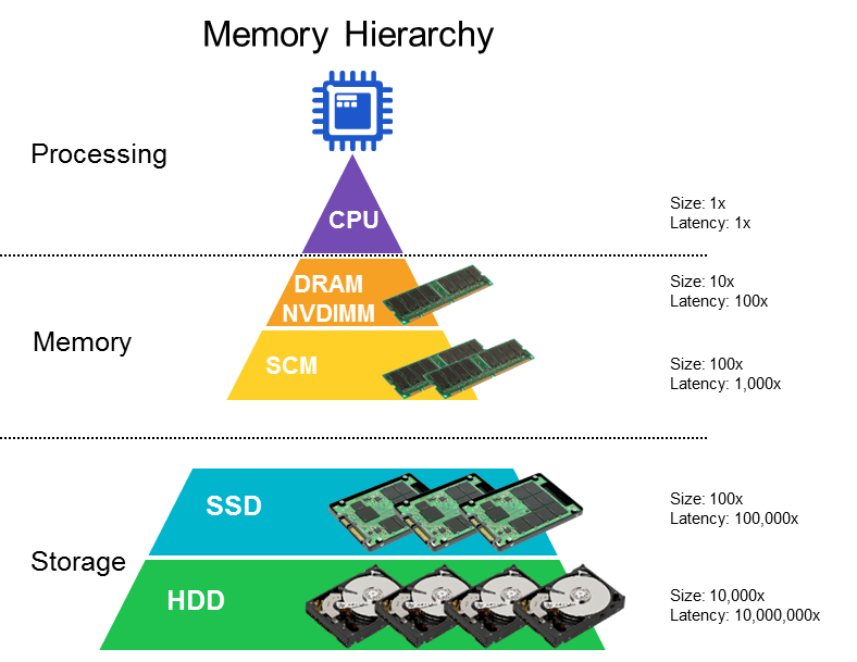 How to determine the CPU power quickly. How to increase the efficiency of the code written by the programmer to execute the CPU even at a low frequency.
How the processor works inside many types of devices
All digital electronic devices are based on a central processing unit (CPU), which is actually the brain of the device. Processors are installed on PC motherboards, routers, game consoles, phones, tablets, NAS and other devices. Learning how a processor works is important for anyone who is about to write software. Also, the information is useful to anyone who is simply interested in the operation of computers. The main parts of the CPU are:
-
Arithmetic logic unit. Performs logical/arithmetic operations (subtraction, addition). Most ALUs include one output or two inputs, but there are varieties with two outputs (such arithmetic logic units are called adders).
-
A control device that allows the CPU to control the operation of the device and perform all the inherent functions.
 CU «tells» the periphery what to do next, coordinating with the rest of the system. There are two options for the control device;
-
using microprogram control (MCU), where the software part is stored in the memory of the CU;
-
hard logic (HCU), where the features of functioning are determined by the structure of the component. Making changes to the way we work is impossible without interfering with the physical structure.
To process instructions, the processor needs data, some of which is intermediate, while others are input / output. The simplest explanation for the functioning of the CPU is the principle outlined by J. von Neumann 75 years ago:
-
Fetch. From the command line register in RAM, the command is read, which will be loaded into the corresponding drive.
-
Decode. Decryption of the incoming command using a decoder, followed by the activation of circuits for execution.
-
Fetch Operands. After loading the values and parameters of commands into mutable registers, the CPU can find the necessary data in RAM, cache memory, or removable media.
-
Execute. Execution of a command by the processor itself or by a peripheral device. At the end of this stage, the cycle repeats.
To increase the efficiency of the code, it is recommended to study how the processor works. You can achieve a certain result with fewer lines of code. This is called optimization, which allows you to reduce the cost and time spent on each task by a computer, microcontroller and other device with a CPU.
CPU instructions
Each instruction represents a calculation that the processor performs. There are several types of commands to execute. All instructions are built into the CPU, and they are generated by the compiler. The instruction set can differ from one line of processors to another, and the cost of manufacturing a CPU directly depends on the number of instructions that the CPU executes.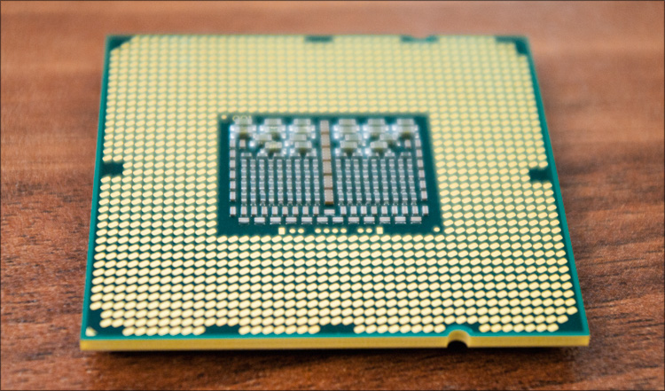
The x86 processor line is backwards compatible, which means that code written on the 8086 or 80486 can be executed using a modern CPU. In this case, the use of emulation is necessary, since the code written for the old processor with a frequency of 4.77 MHz in assembler will run too fast.
How to give a command to the CPU
Any processor «understands» commands in the form of machine code, consisting of the simplest commands (zeros and ones). If you were previously interested in how the processor works, then you already know that the most common way to “communicate” with the processor is to write programs in one of the programming languages:
-
High level. Easy to understand and port code to other devices. The main disadvantage is that it requires a lot of power of the CPU itself for execution. At the same time, the code is not tied to the CPU clock frequency, as is the case with programs written in asm.
-
Low level. The most popular example is assembler.
 This option is more efficient and sparing to the processor resources, but it also requires a higher level of programmer training. Each line of processors has its own assembly language, which is quickly interpreted by the CPU. This programming option was most popular on older computers (Apple II, C64, early Mac generations) and consoles (FamiCom, Mega Drive, Master System).
Clock speed
The speed of any device with a CPU is determined precisely by the clock speed. It represents the number of cycles per second executed by the CPU. The higher the frequency, the faster the device. One cycle is measured in gigahertz, and one GHz is equal to 10 hertz, which indicates 10 cycles per second. To speed up the processor, you can increase the clock speed by overclocking, which is risky — the operation can damage the CPU and even the socket with the motherboard.
How the processor works: a brief introduction
The processor, also known as the microprocessor (CPU), is the heart and/or brain of the computer.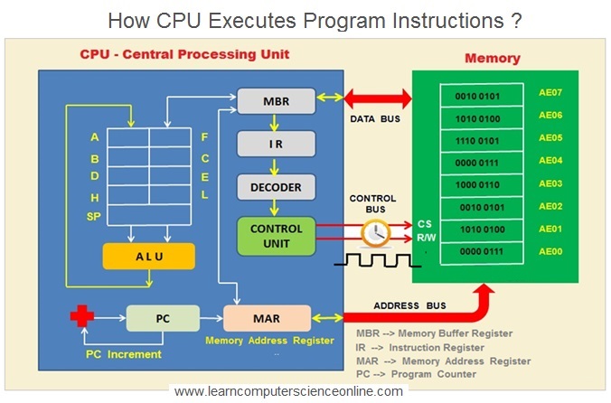 Let’s delve into the essence of the computer to help us write computer programs efficiently.
He follows the instructions given to him. Its main task is to perform arithmetic and logical operations and organize all commands together. Before diving into the main parts, let’s start by looking at the main components of the CPU and their roles:
The two main components of the processor: the control unit — CU, the arithmetic logic unit — ALU
The control unit CU is a part of the CPU that helps organize the execution of instructions. He says what to do. According to the instructions, this helps activate the wires that connect the CPU to other parts of the computer, including the ALU. The control unit is the first CPU component to receive an instruction to process.
The ALU, as the name suggests, performs all arithmetic and logic calculations. ALU performs operations like addition, subtraction, etc.
The main task of the CPU is to execute instructions given to it.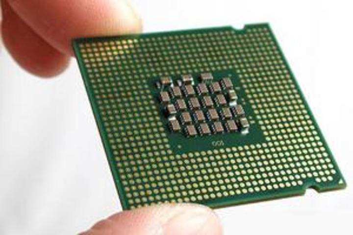 To process these instructions most of the time, data is needed. Some data is intermediate, some is input, and some is output.
Registers
A register is a small set of places where data can be stored. The register is a combination of latches. Latches, also known as flip-flops, are combinations of logic gates that store 1 bit of information.
The latch has two input wires, a record and input wire, and one output wire. We can activate the write wire to make changes to the stored data. When the write wire is disconnected, the output always stays the same.
The CPU has registers for storing output data. Sending to main memory (RAM) will be slow because it is intermediate data. This data is sent to another register that is connected via the bus. A register can store instructions, output data, a storage address, or any other data.
Random Access Memory (RAM)
Ram is a set of registers organized and optimized in such a way that they can store more data.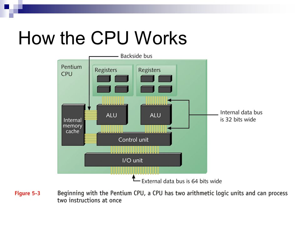 RAM (Random Access Memory) is unstable and its data is lost when we turn off the power. Because RAM is a set of registers for reading/writing data, RAM accepts an 8-bit address input, data input for the actual data to be stored, and finally a read/write activator that works the same as for latches.
Instructions
An instruction is a detailed level calculation that a computer can perform. There are different types of instructions that a processor can process.
Instructions provided to the computer in assembler, generated by a compiler, or interpreted in some high-level languages.
These instructions are built into the processor. The ALU contains an arithmetic and boolean value in which the flow of control is controlled by the CU.
A group of instructions that a computer can execute is called an instruction set.
Processor clock speed
Clock cycle
The speed of a computer is determined by its clock cycle. This is the number of cycles per second that the computer is running. Single cycles are very small, about 250 * 10 * -12 sec. The higher the clock, the faster the processor.
The processor clock cycle is measured in GHz (gigahertz). 1 GHz is equal to 10 Hz (hertz). Hertz means second. So 1 gigahertz means 10 cycles per second.
The faster the clock cycle, the more instructions the processor can execute.
Clock cycle = 1/clock rate
CPU Time = number of clock cycle / clock rate provide to the processor. Some processors provide the ability to increase the clock cycle, but since these are physical changes, overheating and even smoke/fire can occur.
How instruction 9 is executed0328
Instructions are stored in RAM in sequential order. For a hypothetical CPU, an instruction consists of an OP code (operation code) and a memory or register address.
The control block instruction register (IR) has two registers that load the instruction opcode and an instruction address register that loads the address of the currently executing instruction. There are other registers inside the CPU that store the value stored in the address of the last 4 bits of the instruction.
Let's look at an example of an instruction set that adds two numbers. The following are the instructions, along with a description:
STEP 1 - LOAD_A 8
The instruction is initially stored in RAM, say <1100 1000>. The first 4 bits are the opcode. This defines an instruction. This instruction is retrieved in the IR of the control block. The instruction is decoded as load_A, which means it must load data at address 1000, which is the last 4-bit bit of the instruction to register A.0003
STEP 2 - LOAD_B 2
As above, this loads data from memory address 2 (0010) into CPU register B.
STEP 3 - ADD BA
Now the next instruction is to add these two numbers. Here the CU tells the ALU to perform the add operation and store the result back into register A.
STEP 4 - STORE_A 23
This is a very simple set of instructions that helps you add two numbers.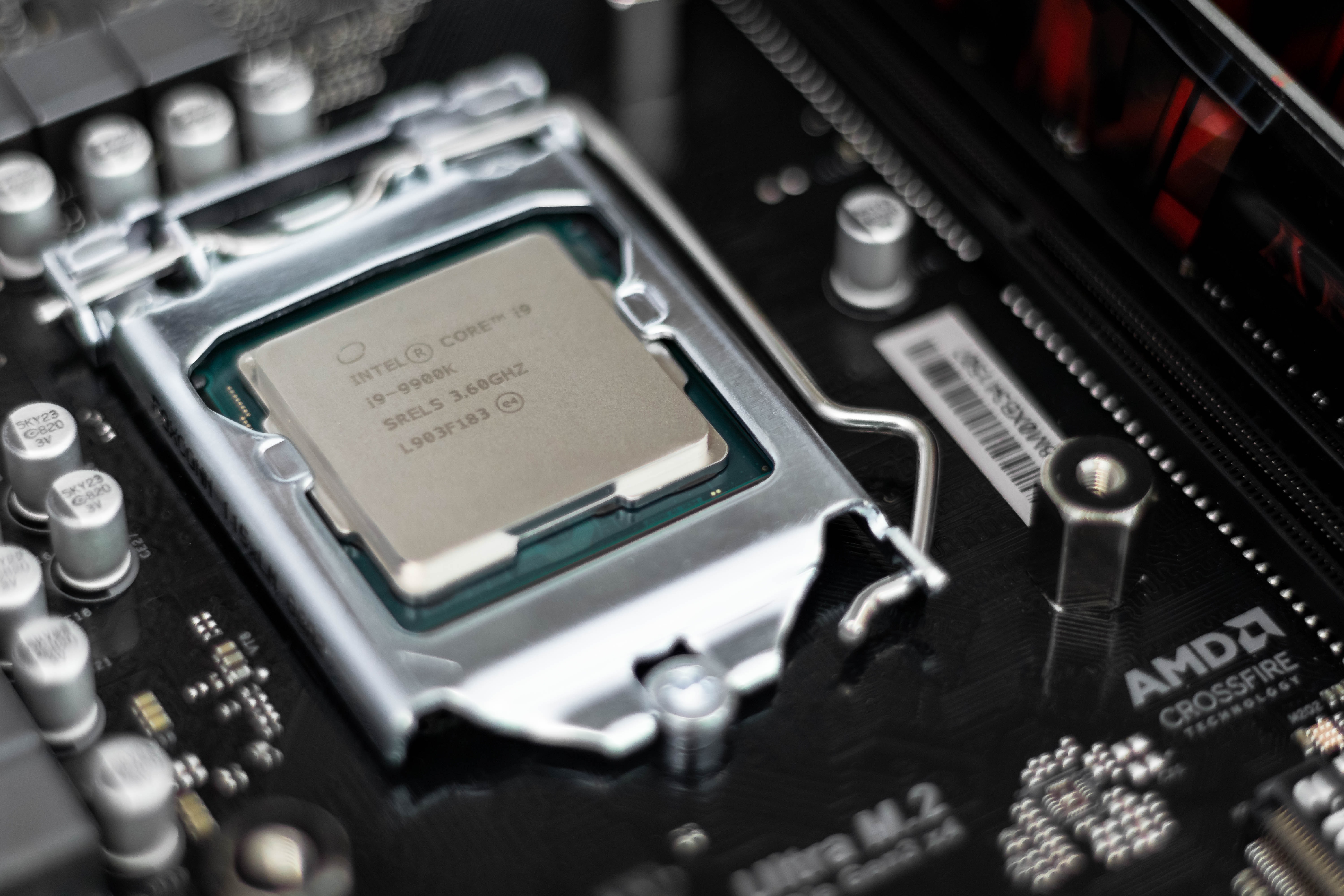
BUS (bus)
All data between the processor, register, memory and I / O device is transferred on the bus. To load the data into the newly added memory, the CPU puts the memory address on the address bus, the result of the summation on the data bus, and turns on the correct signal on the control bus. Thus, the data is loaded into memory using the bus.
The CPU also has a mechanism to preload instructions into the cache. As we know, there are millions of instructions that a processor can execute in a second. This means that it will take longer to fetch instructions from RAM than to execute them. Thus, the CPU cache preselects some instructions as well as data to speed up execution.
If the data in cache and RAM differ, the data is marked as dirty bit.
The modern CPU uses instruction pipelining for parallelization when executing Fetch, Decode, Execute commands. When one instruction is in the decode phase, the CPU can process another instruction for the fetch phase.