Overclocking and Test Setup : ASUS P5E3 Deluxe (Intel X38)
Trending
AMD’s profits are down 93% amidst soft demand for PCs and faltering cryptocurrency markets
Another two top management executives are leaving Apple
Product Listing
- News
- Reviews & Articles
-
Page 1 of 9 — IntroductionPage 2 of 9 — Motherboard FeaturesPage 3 of 9 — Express GatePage 4 of 9 — Overclocking and Test SetupPage 5 of 9 — Results — BAPco SYSmark 2004Page 6 of 9 — Results — Futuremark PCMark05Page 7 of 9 — Results — SPECviewperf 9.0Page 8 of 9 — Results — AquaMark3Page 9 of 9 — Conclusion
Page 4 of 9 — Overclocking and Test Setup
- Next >
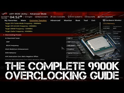
Overclocking
- FSB Settings: 200MHz to 800MHz
- DDR3 Settings: 667/800/835/886/1002/1067/1111/1333MHz
- FSB Strap: 200/266/333/400MHz
- PCIe Settings: 100MHz to 150MHz
- CPU Voltage Settings: 0.
85000V to 1.7000V (in 0.00625V steps)
- Memory Voltage Settings: 1.50V to 2.78V (in 0.02V steps)
- FSB Termination Voltage Settings: 1.20V to 1.50V (in 0.02V steps)
- NB Voltage Settings: 1.25V to 1.91V (in 0.02V steps)
- SB Voltage Settings: 1.05V, 1.20V (in 0.015V)
- Loadline Calibration: Auto (default), Enabled, Disabled
- Ai Clock Twister: Light, Moderate, Strong
- Ai Transaction Booster: Enabled, Disabled
- Multiplier Selection: Yes (unlocked CPUs only)
ASUS seems to be getting better at every aspect of motherboard manufacturing, from better design, to better features, they’ve got a better BIOS as well. We’re not talking about the amount or even granularity of its overclocking features and options (which is plenty really), but option description text that will actually make sense to the user rather than the usual cryptic one-liners. Granted, it is still far from perfect, but we’ve noticed continuous improvements over the past year.
No surprise, the P5E3 Deluxe turned out to be a very competent overclocking motherboard, easily hitting the high 470-480MHz FSB range without the need to increase any chipset voltage. We were able to achieve a maximum stable FSB of 500MHz with a 0.16V increase to the MCH, but the board became unstable beyond that.
Test Setup
Now let’s see what the ASUS P5E3 Deluxe is capable of performance-wise. We compare the new X38 based P5E3 Deluxe to its its predecessor, the P35 based ASUS P5K3 Deluxe as well as some of the competing Intel X38 motherboards around such as Foxconn’s X38A and Gigabyte’s GA-X48T-DQ6. To benchmark these boards, the following hardware configuration will be used:-
- Intel Core 2 Extreme QX6850 processor (3.00GHz)
- 2 x 1GB Kingston HyperX DDR3-1333 @ 7-7-20 CAS 7.0
- Seagate Barracuda 7200.10 200GB SATA hard disk drive (one single NTFS partition)
- MSI GeForce 8600 GTS 256MB — with ForceWare 162.
 18 drivers
 - Intel INF 8.3.1.1013 and AHCI 7.5.0.1017 driver set
- Microsoft Windows XP Professional with Service Pack 2 (and DirectX 9.0c)
Benchmarks
The following benchmarks will be run to determine the performance of the ASUS P5E3 Deluxe:-
- BAPco SYSmark 2004
- Futuremark PCMark05
- SPECviewperf 9.0
- AquaMark3
-
Page 1 of 9 — IntroductionPage 2 of 9 — Motherboard FeaturesPage 3 of 9 — Express GatePage 4 of 9 — Overclocking and Test SetupPage 5 of 9 — Results — BAPco SYSmark 2004Page 6 of 9 — Results — Futuremark PCMark05Page 7 of 9 — Results — SPECviewperf 9.0Page 8 of 9 — Results — AquaMark3Page 9 of 9 — Conclusion
Page 4 of 9 — Overclocking and Test Setup
- Next >
Join HWZ’s Telegram channel here and catch all the latest tech news!
Our articles may contain affiliate links.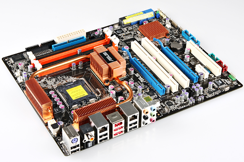 If you buy through these links, we may earn a small commission.
Sponsored Links
P5E3 Deluxe WiFi overclocking | Overclock.net
I’ve got an Asus P5E3 Deluxe WiFi and would like to share some of my overclocking settings with anyone that has this board or anyone considering getting it. I don’t have information on that many CPU/RAM combinations so this is based on what I have. I posted some of this at Asus before.
Overall I’d say that it’s a very good motherboard for stable overclocking. There is plenty of chip cooling thanks to the copper heatsinks it has. The motherboard temperature reading is fairly high by a few degees C (mid 40s) but that’s probably because of the sensor location or BIOS. Keep in mind that my settings are for a quad. It’s a little harder to overclock the quad than a dual so keep that in mind. I’ve been able to get a good frequency/heat/voltage balance at 3. 4GHz with 1001 BIOS and most of the below settings but with higher CPU and NB voltage. That meant more heat for the processor, but I was able to keep it under control at around 48C with a Swiftech LCS.
My system specifications
MB: P5E3 Deluxe WiFi (BIOS 1001)
CPU: Intel Core 2 Quad Q6600, Stepping B3 and Pentium 4 661, Stepping C1
RAM: 2X1GB G.Skill DDR3 1066 Link
CPU cooler: Cooler Master Hyper TX
Power supply: Seasonic M12 700 (new)
Overclock settings for 3.014GHz
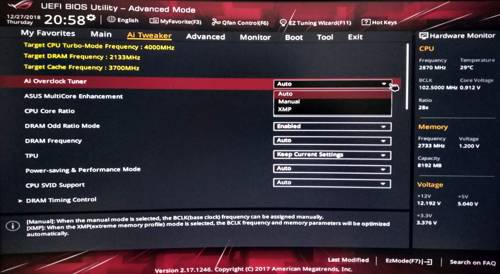
Ai Overclock Tuner: Manual
CPU Ratio Control: 9
FSB Strap to North Bridge: Auto (when enabled try 333)
FSB Frequency: 334
PCIE Frequency: 100
DRAM Frequency: 1072MHz
DRAM Command Rate: 2N (has worked with 1N)
DRAM Timing Control: Manual (7-7-7-18) or 6-6-6-18 with 1.6V
DRAM Static Read Control: Auto
DRAM Static Write Control: Auto
Ai Clock Twister: Auto
Ai Clock Skew for Channel A: Auto
Ai Clock Skew for Channel B: Auto
Ai Transaction Booster: Disabled (worked when enabled at setting 2 but I currently have it off)
CPU Voltage: 1. 31 and 1.325 (1.248 and 1.256 in CPU-Z)
CPU PLL Voltage: 1.6
FSB Termination Voltage: 1.3 (1.3 — 1.5 may work)
DRAM Voltage: 1.5
North Bridge Voltage: 1.5
South Bridge Voltage: 1.05
Clock Over-Charging Voltage: Auto
CPU Voltage Damper (Load-Line Calibration): Auto
CPU Voltage Reference: Auto
North Bridge Voltage Reference: Auto
CPU Spread Spectrum: Disabled
PCIE Spread Spectrum: Disabled
CPU Ratio Control: Manual
C1E Support: Enabled
CPU TM Function: Enabled
Vanderpool Technology: Disabled
Execute Disable Bit: Enabled
Intel (R) SpeedStep (TM) Tech: Disabled (if available)
Speedfan temperature reading at 3.014GHz for CPU is about 50C with Hyper TX.
Overclock settings for 3.2GHz
Ai Overclock Tuner: Manual
CPU Ratio Control: 9
FSB Strap to North Bridge: Auto
FSB Frequency: 356
PCIE Frequency: 100
DRAM Frequency: 1069MHz
DRAM Command Rate: 2N (has worked with 1N)
DRAM Timing Control: Manual (7-7-7-18 and 7-7-7-20) or 6-6-6-18 with 1. 6V
6V
DRAM Static Read Control: Auto
DRAM Static Write Control: Auto
Ai Clock Twister: Auto
Ai Clock Skew for Channel A: Auto
Ai Clock Skew for Channel B: Auto
Ai Transaction Booster: Enabled — Boost Level 2 (also works when disabled)
CPU Voltage: 1.36 (1.33 in CPU-Z)
CPU PLL Voltage: 1.6
FSB Termination Voltage: 1.5
DRAM Voltage: 1.5
North Bridge Voltage: 1.5
South Bridge Voltage: 1.05
Clock Over-Charging Voltage: Auto
CPU Voltage Damper (Load-Line Calibration): Auto (also works when enabled)
CPU Voltage Reference: Auto
North Bridge Voltage Reference: Auto
CPU Spread Spectrum: Disabled
PCIE Spread Spectrum: Disabled
CPU Ratio Control: Manual
C1E Support: Enabled
CPU TM Function: Enabled
Vanderpool Technology: Disabled
Execute Disable Bit: Enabled
Intel (R) SpeedStep (TM) Tech: Disabled (if available)
Speedfan temperature reading at 3.2GHz for CPU is is about 52C with Hyper TX.
Here goes what I»ve been able to do with my Pentium. ..
..
Stable overclock settings with Pentium 4 661 @ 4.5GHz
FSB Frequency: 250
Ai Transaction Booster: Enabled at level 2
CPU Voltage: 1.28V (1.256V in CPU-Z)
CPU Voltage Damper (Load-Line Calibration): Enabled
RAM voltage: 1.6V
North Bridge Voltage: 1.35
RAM settings: 1003 MHz 6-6-6-18 1N. All other RAM settings at auto
C1E Support: Enabled
CPU TM Function: Enabled
Execute Disable Bit: Enabled
Intel (R) SpeedStep (TM) Tech: Disabled
Reactions:
noneed4me2
JavaScript is disabled. For a better experience, please enable JavaScript in your browser before proceeding.
1 — 9 of 9 Posts
noneed4me2
·
Registered
noneed4me2
·
Registered
subzer0
·
Registered
subzer0
·
Registered
subzer0
·
Registered
subzer0
·
Registered
noneed4me2
·
Registered
subzer0
·
Registered
1 — 9 of 9 Posts
- This is an older thread, you may not receive a response, and could be reviving an old thread.
 Please consider creating a new thread.
Join now to ask and comment!
Continue with Facebook
Continue with Google
or
sign up with email
Top
FAQ OC and BIOS setup
What you need to do before you start working with MOBO:
1.
Read ASUS P5E (Intel X38) motherboard review. Here we learn about the stock thermal interface and overclocking via SetFSB, we do not pay attention to the information about the possibility of flashing the BIOS from the older model (at the moment there are no difficulties with the firmware to the older model) and about the lack of direct access to
Performance Level (Author’s error)
2. Check if your CPU is supported by BIOS versions. In the same place, we pay attention from which BIOS version this or that CPU is supported:
P5E
P5E Deluxe
P5E3
P5E3 DELUXE
P5E3 Premium
P5E3 WS Professional
P5E64 WS Professional
P5E64 WS EVOLUTION
Maximus Formula
Rampage Formula 9000 CPU3 starts because the factory-wired BIOS version is outdated and does not support the latest CPU models. To solve this problem, you need a processor, for example, the E2xxx / E4xxx / E6xxx series — with them you can easily start and flash a new BIOS
3.
Pay attention to the following plate — MOBO tends to overestimate some voltages, for 65nm the CPU FSB Termination Voltage is overestimated and underestimated for 45nm CPU
voltage values in [auto] can lead to degradation / death of the CPU E8xxx / Q9xxx :
| Bios Set | Set Manual | Monitoring | Idle/full Load Multimeter |
|---|---|---|---|
| Vcore | 1.600 | 1.544 | 1.555/1.493 |
| CPU PLL | 1.800 | 1.912 | 1.846/1.845 |
| NB | 1.730 | 1.76 | 1.720/1.717 |
| DRAM | 2.5 | 2.608 | 2.583/2.578 |
| FSB | 1.600 | 1.680 | 1.647/1.646 |
| SB | 1.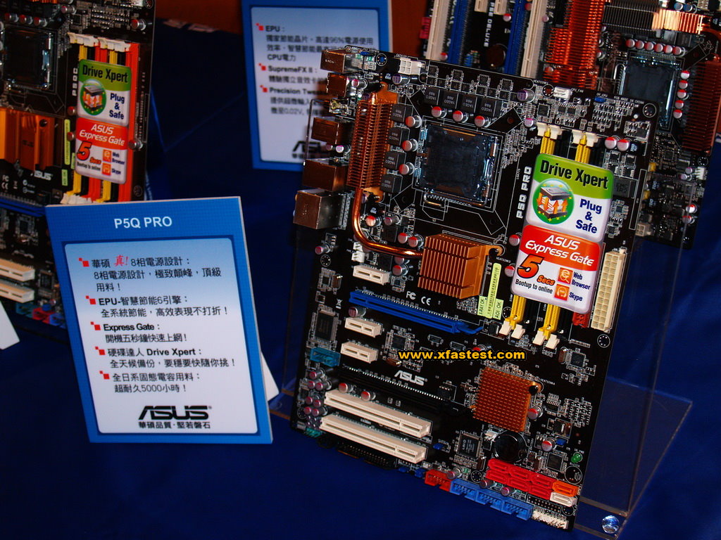 175 175 |
1.216 | 1.175/1.174 |
| SB 1.5V | 1.850 | 1.904 | 1.838/1.833 |
4.
DDR/FSB dividers :
| First divider | Second divider | |
|---|---|---|
| FSB Strap | DDR/FSB | DDR/FSB |
| 200 (Need Vnb>1.6V) | 5:3 | 2:1 |
| 266 (Need Vnb>1.45V) | 5:4 | 3:2 (max FSB=425-430) |
| 333 | 1:1 | 6:5 |
| 400 | 1:1 | 4:3 (max FSB=460-470) |
5.
Which divisor is better to choose, read here
6.
Operable PL values for FSB=[400-450]MHz for x38 (tested by
Spyrus )
7. I think it’s worth posting the correspondence of PL to the voltage on NB, this plate will be updated as data becomes available
| FSB | Strap | Divider | DDR Speed | Timings | PL | AI Clock Twister | Memory Speed | FSB Memory Data Speed |
Latency | Vnb |
|---|---|---|---|---|---|---|---|---|---|---|
| 500 | 333 | 6:5 | 1200 | 5-5-5-12 | 8 | Moderate | 10 3xx | 106xx | 50-51 | 1. 39 39 |
| 500 | 333 | 6:5 | 1200 | 5-5-5-12 | 7 | Moderate | 106xx | 106xx | 47-48 | 1.61 |
| 400 | 333 | 1:1 | 801 | 4-4-4-10 | 7 | Stronger | 8 2xx | 84xx | 60-61 | 1.35 |
| 400 | 266 | 3:2 | 1200 | 5-5-5-12 | 7 | Moderate | _ | _ | 60-61 | 1.59 |
| 400 | 266 | 3:2 | 1200 | 5-5-5-12 | 6 | Moderate | _ | _ | 54-55 | 1.71 |
8.
What is Det RAM — if you see a black screen after successfully passing the tests, this is the Det RAM error. The error is called Det RAM because the post-indicator writes Det RAM when the system stops. The nature of this error remains unclear, and the methods of struggle have not been finally established. You can try 2 ways that sometimes work:
a) Raise the PCI-E frequency to 110-112MHz (leads to additional GPU heating)
b) Set all DDR2 … REF Voltage values to [+0.10] or more
9.
Where can I download fresh firewood for the motherboard?
Chipset Drivers
Hard Disk Controller Drivers
Network Controller Drivers
JMicron Controller Drivers
Soundcard Drivers
CPU Overclocking:
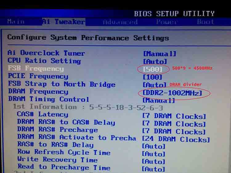
First of all, we need to minimize the influence of memory parameters on CPU overclocking.
We go in the BIOS settings to the page
AI Tweaker and set the following parameters
AI Clocker Tuner: [Manual] —
CPU Ratio Control: [Auto] . This parameter is used to fix possible CPU multipliers, it is also duplicated in the CPU tab.
FSB Strap for North Brige: [400] . The parameter for switching the operating modes of the memory controller. A 1:1 divider is possible on FSB Strap [333] and [400] — but on FSB Strap: [400] the NB clock generator is less stressed, so we choose it
FSB Frequency — the main overclocking tool, first set by default for your processor. As a rule, for modern processors this can be 200/266/333
Dram Frequency — We set the smallest number from the drop-down list available with the FSB Strap for North Brige [400]. This will be the divisor for 1:1 memory. It is worth noting that, for example, with a value of FSB = 500, your memory will operate at an effective frequency of 1000MHz (PC8000), so you need to take care of the memory modules 100% operating at the expected frequencies during overclocking
PCIE: [100] Fix the frequency of the PCI-E bus. This parameter does not apply to memory, but we will also fix it so that it does not interfere with CPU overclocking.
DRAM Command Rate : [2T]
DRAM CLK Skew on Channel A : [Advanced 350] — delay time for CPU access to memory channel A in ps (1picosecond=one trillionth of a second). You can read a little about this option.
here. I recommend putting [
Advanced 350 ] for both channels
DRAM CLK Skew on Channel B : [Advanced 350] — delay time for CPU access to memory channel B in ps (1picosecond=one trillionth of a second)
DRAM Timing Control: [Manual]
CAS# Latency : [5]
RAS# to CAS# Delay : [5]
RAS# Precharge : [5]
AS# 15]
RAS# to RAS# Delay : [Auto]
Row Refresh Cycle Time : [Auto]
Write Recovery Time : [Auto]
Read to Precharge Time : [Auto]
Read to Write Delay (S/D) : [Auto] — Together with the two sub-items, it is responsible for the speed of copying in memory within the limits defined by CAS#
Write to Read Delay (S) : [Auto]
Write to Read Delay (D) : [Auto]
Read to Read Delay (S) : [Auto] — Delay between Read-Read cycle from one bank to the same. Responsible for the read speed in memory within the limits defined by CAS#
Read to Read Delay (D) : [Auto] — Delay between the «Read-Read» cycle from one bank to another within the limits defined by CAS#
Write to Write Delay (S) : [Auto] — Delay between «Write-Write» cycle from one bank to the same. Responsible for the write speed in memory within the limits defined by CAS#
Write to Write Delay (D) : [Auto] — Delay between the «Write-Write» cycle from one bank to another within the limits defined by CAS#
Write to PRE Delay : [Auto]
Read to PRE Delay : [Auto]
PRE to PRE Delay: [Auto]
ALL PRE to ACT Delay: [Auto]
ALL PRE to REF Delay: [Auto]
DRAM Static Read Control: [Disabled] — read
here .
If set
DRAM Static Read Control=[auto] and
Transaction Booster=[auto] , then the BIOS itself will set the minimum possible PL, according to the BIOS, for boards
P5E it is recommended to do just that
AI Clock Twister : [Moderate] — NB operating mode, changes the internal delays of the NB, Moderate — by default
Transaction Booster : [Manual] — Allows direct access to Performance Level (tRD) settings — one of the most important memory controller performance factors for Intel systems.
For P5E/Maximus formula bios set: Transaction Booster [Disabled] Relax Level [3]
C/P: A1 A2 A3 A4 A5 | B1 B2 B3 B4 B5
LVL: 10 10 10 10 10 | 10 10 10 10 10 displays the actual Performance Level settings for individual memory access phases
Common Performance Level [10] — directly setting the PL itself on the memory access cycle as a whole
Pull-In of CHA Ph2 Disabled — The parameter enables memory access acceleration for a single phase by setting the phase to value=[PL-1]. If you set PL=8 and enable Pull-In on all phases, then in fact the memory is accessed at PL=7 settings. The greatest increase in performance gives the inclusion of acceleration for both channels in the first phase and the smallest for the last.
Pull-In of CHA Ph3 Disabled
Pull-In of CHA Ph4 Disabled
Pull-In of CHA Ph5 Disabled
Pull-In of CHB Ph3 Disabled
Pull-In of CHB Ph4 Disabled
Pull-In of CHB Ph5 Disabled here, for starters, set the value equal to the VID of your processor instance
CPU PLL Voltage: [1. 5] — determines the supply voltage of the Phase Locked Loop system (PLL or PLL — Phase Locked Loop) and is relevant only to improve the stability of overclocked quad-core processors. In most cases, the smallest value is sufficient. The default value is 1.5. Increasing the value sometimes helps in overclocking, but according to personal observation, it leads to the opposite — the near-socket space is wildly heated. I do not recommend using values higher than 1.6
North Bridge Voltage : [1.55]
DRAM Voltage [???] — depends on your memory, 2.2V is fine for microns.
with values in the BIOS above 2.16, I recommend equipping the airflow of the memory modules, otherwise degradation of the modules is possible
FSB Termination Voltage : [1.24] — for me personally, this value is enough for the linpak to pass the system by 500 * 8, but for quads it can be increased to 1.3-1.36.
South Bridge Voltage : [1.05] — also sufficient value for overclocking to FSB=500-520MHz. For RAID arrays, you may need a little more
Loadline Calibration : [Enabled] — in the Enabled position, the parameter allows you to avoid CPU Voltage drop in the load, thereby increasing overclocking stability.
For motherboards on the x48 chipset, it is recommended to disable this option (bug found)
CPU GTL Reference : [0.67X] GTL Reference Voltage is the system bus signal voltage, which is a derivative of CPU VTT voltage. The latter, in turn, is used to start the processor and power the I / O buffer circuits. In any case, such a definition is given by the documentation for the voltage management module (VRM) for motherboards with support for modern Intel processors. Allows you to increase the overclocking potential of the CPU. who is interested in theory — read
here. Together with
GTL Reference recommended to increase
FSB Termination Voltage up to 1.3-1.4V for latest generation CPUs and up to 1.35-1.45v for Quads
North Bridge GTL Reference : [0. 67X] — comparable to the previous paragraph, the current acts on the north bridge (memory controller)
DDR2 Controller REF Voltage : [DDR2_REF+10] — voltage for memory controller
DDR2 Channel A REF Voltage : [DDR2_REF+10]
DDR2 Channel B REF Voltage : [DDR2_REF+10]
SB 1.5V Voltage : [1.5]
NB LED Selection : [NB Volt]
SB LED Selection : [SB Volt]
[Disabled]
CPU Spread Spectrum : [Disabled] — Spread Spectrum Modulated — Enabling this setting reduces electromagnetic emissions from the computer by reducing clock oscillator glitches. The reduction can be up to 6%. It should be noted that this may adversely affect the operation of waveform-sensitive devices, so it is recommended to enable this parameter only when testing computers for electromagnetic compatibility. Disable for overclocking
PCIE Spread Spectrum : [Disabled] same as above, only valid for PCI-E bus
After applying the above parameters, we decouple as much as possible the dependence of overclocking on memory capabilities.
Now you can take on the overclocking of the CPU itself
After each successful boot, I raise the FSB value in 10-15MHz increments and try to boot again. If, after another increase in the FSB value, the system refuses to boot, press the «Power» button on your system unit for 4-6 seconds. After that, the system will boot at default frequencies with a message about unsuccessful overclocking. Press F1 and in the BIOS settings we raise the CPU Voltage value (I do this in increments of 0.01-0.015V).
After multiple reboots, we hit some limit. This will be the limit of permissible temperatures (60-65 degrees on the CPU cover) or the limit of reasonable CPU Voltage values \u200b\u200b(for modern CPUs it will be 1.5-1.6V, for E8xxx — 1.4-1.5V.
It remains only to fix the achieved result — to pass stability tests for the system in overclocking. For tests, I use the Linpack utility from Intel. If the test gives errors, we try to slightly increase the CPU Voltage, and if it doesn’t help, we lower the FSB value a little to stable values.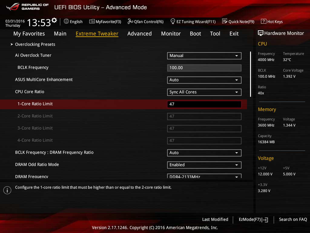
I would like to dwell on testing in more detail. After overclocking the CPU, it is necessary to test the CPU, because in the future, when configuring the memory operation, we will not be able to determine the cause of failures — errors can be caused by both the memory and the CPU. Therefore, having put the CPU overclocking configuration in order, we take the latest version
Linpack. Unpack the w_lpk_p_10.0.2.005.zip folder: linpack_10.0.2\benchmarks\
linpack . For 32-bit operating systems, open the file in a text editor
lininput_xeon32 (
lininput_xeon64 for x64 OS) and edit. The content should look like this:
Sample Intel(R) LINPACK data file (lininput_xeon32)
Intel(R) LINPACK data
1 # number of tests
14000 # Matrix size for testing with 2Gb of memory (13000 for x64 OS), for 4 GB change the value to 20000
14000 # leading dimensions. Repeating the value from the above paragraph
10 # Number of test passes.
4 # alignment values (in KBytes)
The number of passes must be at least 5 or we will not be able to detect a system failure
After editing the file
lininput_xeon32 save it and run the file
runme_xeon32.bat (
runme_xeon64.bat for x64 OS)
During the passage, we monitor the temperature regimes of the CPU — do not forget about the dangerous temperature of 60-65 degrees on the CPU cover (75-80 on the cores). If during the test the temperatures exceed this threshold, it is better to interrupt the test and think about how to cool the CPU more efficiently or reduce overclocking
At the end of the test, the window will close. We can see the results in the file
win_xeon32.txt (
win_xeon64.txt for x64 OS).
Here we have to compare the values in the columns
Residual and
Residual(norm) . As a rule, each system will have its own values, but the values in each column should be the same. If you have different values, you definitely have failures and you need to fine-tune the system. For clarity, the screen of the correct passing of the Linpack tests:
My settings from the screen above for E8200 500×8:
AI Clocker Tuner: [Manual]
CPU Ratio Control: [Auto]
FSB Strap for North Brige: [333]
FSB Frequency: [500]
Dram Frequency: [1201]
PCIe: [112]
DRAM Command Rate : [2T]
DRAM CLK Skew on Channel A : [Normal]
DRAM CLK Skew on Channel B : [Normal]
DRAM Timing Control: [Manual]
CAS# Latency : [5]
RAS# to CAS# Delay : [5]
RAS# Precharge : [5]
RAS# ActivateTime : [12]
RAS# to RAS# Delay : [Auto]
Row Refresh Cycle Time : [35]
Write Recovery Time : [5]
Read to Precharge Time : [Auto]
Read to Write Delay (S/D) : [Auto]
Write to Read Delay (S) : [Auto]
Write to Read Delay (D) : [Auto]
Read to Read Delay (S) : [Auto]
Read to Read Delay (D) : [Auto]
Write to Write Delay (S) : [Auto]
Write to Write Delay (D) : [Auto]
Write to PRE Delay : [Auto]
Read to PRE Delay : [Auto]
PRE to PRE Delay : [Auto]
ALL PRE to ACT Delay : [Auto]
ALL PRE to REF Delay : [Auto]
DRAM Static Read Control: [Disabled]
AI Clock Twister : [Moderate]
Transaction Booster : [Manual]
C/P: A1 A2 A3 A4 A5 | B1 B2 B3 B4 B5
LVL: 07 08 07 07 07 | 07 08 07 07 07
Common Performance Level [8]
Pull-In of CHA Ph2: [Enabled]
Pull-In of CHA Ph3: [Disabled]
Pull-In of CHA Ph4: [Enabled]
Pull-In of CHA Ph5: [ Enabled]
Pull-In of CHB Ph5: [Enabled]
Pull-In of CHB Ph2: [Enabled]
Pull-In of CHB Ph3: [Disabled]
Pull-In of CHB Ph4: [Enabled]
Pull-In of CHB Ph5: [Enabled]
Pull-In of CHB PH5: [Enabled]
CPU Voltage : [xxx]
CPU PLL Voltage : [1. 5]
5]
North Bridge Voltage : [1.55]
DRAM Voltage [2.16]
FSB Termination Voltage : [1.3]
South Bridge Voltage : [1.1]
Loadline Calibration : [Enabled]
CPU GTL Reference : [0.67X]
North Bridge GTL Reference : [0.67X]
DDR2 Controller REF Voltage : [DDR2_REF]
DDR2 Channel A REF Voltage : [DDR2_REF]
DDR2 Channel B REF Voltage : [DDR2_REF]
SB 1.5V Voltage : [1.5]
NB LED Selection : [NB Volt]
SB LED Selection : [SB Volt]
CPU LED Selection : [CPU Volt]
Voltiminder LED : [Disabled]
CPU Spread Spectrum : [Disabled]
PCIE Spread Spectrum : [Disabled]
[CPU Configuration]
CPU Ratio Control: [Auto]
C1E Support: [Enabled]
CPUTM: [Enabled]
Vanderpool Technology: [Disabled]
Execute Disable Bit: [Disabled]
Intel SpeedStep: [Enabled]
Examples of settings for subjects on DDR3:
471*7 from
Gre4ka
411*9from
V. I.V.
I.V.
This article is not absolute in all manifestations, but I hope it will help you get acquainted with the principles of overclocking for motherboards from
Asus .
Subscribe to our channel in Yandex.Zen or telegram channel @overclockers_news — these are convenient ways to follow new materials on the site. With pictures, extended descriptions and no ads.
ASUS P5E3 and ASUS P5E3 Deluxe — Let’s say «no» to unification — Ferra.ru
» what is a top product. Boards based on high-level chipsets were not mass-produced, much less cheap, but exclusive features that affordable solutions did not have reserved their place in fairly expensive systems. In the fall of 2007, another change of the company’s flagship came, the role of which fell to the representative of the Intel 3 Series line. The capabilities of the X38 system logic set, namely, it replaced the “old man” i975X, we already considered in last year’s material, but we will try to briefly recall its characteristics.
So, the new product from Intel actually differs from the previously presented P35 by supporting the PCI Express 2.0 bus, which provides twice the bandwidth compared to PCI-E 1.x, and the mode of operation of the CrossFire technology, which operates according to the formula «PCI-E x16 + PCI -E x16». The memory controller was also slightly redesigned and support was added for a proprietary extension to the SPD of DDR3 modules called XMP (eXtreme Memory Profiles), similar to NVIDIA’s EPP. For better cooling and security, the manufacturer has provided the X38 chip with a heat-distributing cover, which is not available on other 3-series chipsets. In terms of other indicators, the high-end solution repeats the same P35, namely: it supports new 45-nm processors, FSB up to 1333 MHz, DDR2-800 and DDR3-1333 memory. The familiar ICH9 is used as the south bridge.R, announced with a new line of chipsets.
Today we’ll review two motherboards manufactured by ASUS based on Intel X38, belonging to the P5E series, but representing different model ranges. The ASUS P5E3 board is positioned as an affordable solution with DDR3 support, while the ASUS P5E3 Deluxe is already designed for more demanding users.
Board specifications
| INTEL Core 2 Quad, Core 2 Extreme, Core 2 Duo, Pentium Dual-Core (E), Pentium Extreme Edition, Pentium D, Pentium 4 | The maximum front tire frequency (FSB), MHz | 1333/1066/800 | 1600*/1333/1066/800 | ||||||||||||
| Maintened memory | type | DDR type | DDR type | DDR type | DDR0039 | ||||||||||
| Memory frequency range, MGC | 1800*/1600*/1333/1066/800 | 1800*/1600*/1333/1066/800 | |||||||||||||
| The number of memory slots 40039 | 4 | 4 | |||||||||||||
| Support for dual-channel operation (if two modules are installed) | + | + | |||||||||||||
| 0039 | 2 | 2 | |||||||||||||
| The maximum volume of supported memory, GB | 8 | 8 | |||||||||||||
| Support for register memory modules | — | — | — | — | — | — | — | — | — | — | — | — | ECC) | — | — |
| Chipset | |||||||||||||||
| Chipset modification | Intel X39 | Intel X380027 | COM Ports | 1x on the board | 1x on the board | ||||||||||
| LPT Ports | — | ||||||||||||||
| PS \ 2 Ports | 1x on the panel (for the keyboard) | ||||||||||||||
| FireWire (IEEE 1394) ports | 2 = (1x on panel + 1x on board) | 2 = (1x on panel + 1x on board) | |||||||||||||
| Game port (MIDI) 39 — 9038 | — | ||||||||||||||
| 6x SATA II (3 GB/s) | 6x SATA II (3 GB/s) | ||||||||||||||
| The ability to form the RAID masses at the BIOS level in the first controller | + | ||||||||||||||
| levels RAID | 0, 1, 5, 10 | 0, 1, 5, 10 | |||||||||||||
| Second Controller | Marvell 88SE6111 | JMICRON JMB363 | |||||||||||||
| The number of lines UDMA 133 on the second controller | 1 for 2 devices for 20039 | + | + | ||||||||||||
| The availability of a connector on the board for connecting additional devices (AUX_IN) | — | — | |||||||||||||
| The presence of connectors for connecting the frontal panel | + | + | + | + | + | + | + | + | + | + | + Motherboard Power | ||||
| ATX Primary Connector | ATX 24-pin | ATX 24-pin | |||||||||||||
| 8 4 / 6 / 6 Pin Auxiliary Connector0039 | + \ — \ — | — \ — \ + | |||||||||||||
| CPU PSU Complexity | High (8-phase power) | High Cool (8-phase power) | |||||||||||||
| The number of exits to the coolers | 4 | 6 | |||||||||||||
| Coolery exits | 1x — four -contactive | 1x — four -term0039 | |||||||||||||
| North bridge cooling | Passive using a heat tube | Passive using a heat tube | |||||||||||||
| Southern bridge cooling | Passive using a heat of stamina | ||||||||||||||
| Passive with heatpipe + separate heatsink | Passive with heatpipe
905 even for the remote control familiar to us from the ASUS P5B Premium Vista Edition, which connects to a specially dedicated USB connector on the rear panel (the necessary port is marked on the I / O Shield bar). But as far as we remember, Deluxe models always had a richer package and had additional functionality. In our case, the kit is almost the same, which means that the differences between the products in question should lie precisely in the functionality, which we will now check. Inspecting the boards So, both boards are designed to install processors from both the Core 2 family and its derivatives such as Pentium Dual-Core and Celeron. The old Pentium/Pentium D with a bus from 800 MHz and, of course, a 45-nm CPU based on Wolfdale and Yorkfield are also not forgotten. The option to install a Celeron Dual Core is also provided, but it seems impossible to see the X38+Celeron combo, except on test machines. The rear panels of the P5E3 and P5E3 Deluxe differ only in the absence of a second network connector and one eSATA on the more affordable version. Otherwise, they repeat each other: one PS / 2, six USB ports, optical and coaxial S / PDIF, FireWire connector, RJ45 and eSATA, as well as 6 audio connectors. On this note of product similarity, we have to finish, because further on these are completely different boards, unlike the considered P5K series, in which even the model with DDR3 support has the same PCB design. ASUS P5E3Black textolite, which in the days of ASUS CUSL2-C Black Perl added prestige to products, has ceased to be something outstanding, but, nevertheless, has not lost its purpose. Agree, because black boards look much more presentable than ordinary boards. The design of ASUS P5E3 has both positive and negative sides, and not only ASUS products suffer from such shortcomings. The negative points include the proximity of the DIMM slots to the first PCI-E x16 slot, which will not allow you to remove memory modules without removing the video card. Another very interesting design decision — the company’s engineers for some reason considered the installation of a COM port in the upper right corner of the board the most convenient place to place it, although it would be problematic to find a rack with such a long cable. Now about the pluses, and not only the design plan. As befits a high-end product, ASUS P5E3 is equipped with an eight-channel processor power supply using high-quality components, as in all other power circuits. The power transistors responsible for 4 channels are covered with a separate aluminum radiator, the rest of the elements are already cooled by a complex-shaped radiator connected by a heat pipe to the chipset microcircuit cooling system. The heat sink on the ICH9R chip is made with ribs, and in this case, the presence of a heat pipe seems meaningless, but, given the general fashion for a heat pipe, when a high-level solution simply has to be equipped with intricate plexuses of tubes and radiators, nothing is surprising here. The X38 chip has a small heatsink with a futuristic-looking cover with a printed company logo. There are four connectors on the board for connecting fans, one of which is a 4-pin connector for a processor fan. After clarifying all the serious shortcomings, let’s return to the positive points. All other connectors and connectors are located at the edges of the board and quite thoughtfully. So, the floppy drive connector is located at the top of the board; IDE connectors and two pairs of SATA opposite the PCI-E x16 slots are rotated 90°, which will allow you to install video cards like GeForce 8800GTX/Ultra or Radeon HD 3870 X2. If it turns out that the HDD cage in the case is located close to the board, then two standard SATA connectors will allow you to connect cables in the usual way. ASUS P5E3, as expected from an X38-based product, has two PCI-E x16 slots. To expand the functionality, two more regular PCI and two PCI-E x1 are installed, although the native functionality of the board still lags behind some solutions based on the younger representatives of the Intel 3 Series chipset family. Only one network controller (Marvell 88E8056) is installed on this model, and the optional Marvell 88SE6111 chip supporting one IDE channel allows you to connect only one eSATA device. The presence of the south bridge ICH9R, which supports 6 SATA II channels with the ability to organize RAID arrays 0, 1, 5, 10, alleviates the lack of external interfaces for connecting a HDD. ASUS P5E3 DeluxeAnother «black prince», but more functional and with some shortcomings, both old and new. As in the first case, the memory slots are close to PCI-E x16, although the graphical interface has shifted to the right. The COM port is already installed in the usual place — in the lower left corner. The rest of the peripheral connectors are neatly placed along the edges of the board, in much the same way as in the more affordable model. Note the rearranged IDE and SATA connectors — now they are in a «mirror image». The processor power subsystem is made according to an 8-channel scheme, all capacitances on the board are solid-state, coils are in ferrite cases. The auxiliary power connector is now EPS12V standard, which will allow you to easily overclock the Core 2 Quad. And, of course, the cooling system has undergone significant changes: the radiator on the north bridge has become more impressive; on the ICH9R, the cooling element is a conventional heat sink; the cooling elements of all power elements are part of the CO connected by a heat pipe, and another radiator has been added above the EPU controller. The ClearCMOS jumper is no longer adjacent to the FrontPanel, but is located on the bottom edge of the board, and after installing ASUS P5E3 Deluxe in some cases, using the jumper will be extremely inconvenient. Now we have come to the main distinguishing feature of the Deluxe version from the regular version, namely the functionality of the board. If in the P5E3 model only two PCI-E x16 slots were available to the user (and, logically, no more are needed), then in this case, engineers increased the number of slots to three, two of which support 16 PCI Express 2.0 lanes each, and one , black and located on the edge of the board, — a total of 4 PCI-E lanes. Nothing is yet known about the possibility of installing a third video card in CrossFireX mode (at the moment, even Catalyst drivers do not support this function), even if it appears, you should not forget that when x4 mode is activated, a couple of additional PCI-E x1 slots will turn off. Of the additional chips that expand functionality, the board has two gigabit network controllers, and one of them (Realtek RTL8110SC) is located on the PCI bus, which reduces its efficiency. This is due to the presence of a PCI-E slot operating in x1 / x4 mode, and, as you know, the south bridge supports only 6 PCI Express lines, two of which are already occupied by the second network controller on Marvell 88E8056 and the HDD controller — JMicron JMB363 (1 channel IDE and 2 SATA II channels). The sound subsystem is based on the already familiar 10-channel HD audio codec ADI AD1988B with a signal-to-noise ratio of 101 dB, which is quite enough for an integrated solution. As you can see, the price difference between the regular and Deluxe version includes a more powerful CO, 4 pins in an additional power connector, a second cooler, another PCI-E x16 slot, also one eSATA channel and a network controller, a better audio codec. BIOSThe BIOS of both boards, based on AMI microcode, allows you to fine-tune the system for yourself, as in all ASUS products aimed at enthusiasts and demanding users. Overclockers have the opportunity to raise the FSB to 800 MHz in 1 MHz steps, raise the voltage on the processor to 1.7 V, on the system bus — up to 1.5 V, memory — up to 2.3 V (2.78 V for P5E3 Deluxe) . In a more expensive model, there is such a parameter as Clock Over-Charging, thanks to which you can increase the stability of the FSB bus when it is overclocked. | ||||||||||||||
| The number of controlled power lines | 4 | 4 | |||||||||||||
| The number of controlled cooling lines (temperature) | 2 | 2 | |||||||||||||
| The number of controlled coolering lines (cure) | 5 | ||||||||||||||
| Cooler speed versus temperature system | Yes | Yes | |||||||||||||
| Possibility to turn off the system in case of overheating | Yes, functions only on processors with an unlocked multiplier | ||||||||||||||
| Frequency change (in what range and in what step) | |||||||||||||||
| 200 MHz to 800 MHz in 1 MHz steps | |||||||||||||||
| Bus frequencies | PCI Express — 100 MHz to 150 MHz in 1 MHz steps | PCI Express — 10 MHz to 10 MHz 1 MHz steps | |||||||||||||
| Memory frequency | 533/639/667/709/800/800/852/887/1066MHz | 533/667/709/800/852/887/1066MHz | |||||||||||||
| Change within what limits and in what steps) | |||||||||||||||
| To the CPU | From 1. 10000 V to 1.70000 V in steps of 0.00625 V 10000 V to 1.70000 V in steps of 0.00625 V |
From 1.10000 V to 1.70000 V in steps 0.00625 V | |||||||||||||
| To FSB, PCI-Express or others | FSB: 1.20V to 1.50V in 0.02V steps SB: 1.05V/1.20V CPU PLL: 1.50V to 1.78V with 0.02V steps | FSB: 1.20V to 1.50V 0.02V steps SB: 1.05V/1.20V CPU PLL: From 1, 50V to 2.78V in 0.02V steps Clock Over-Charging: 0.70V to 1.00V in 0.10V steps | |||||||||||||
| To memory modules | From 1, 50 V to 2.30 V in 0.02 V steps | 1.50 V to 2.78 V in 0.02 V steps | |||||||||||||
| At NorthBridge | 1.25V to 1.75V in 0.02V steps | 1.25V to 1.91V in 0.02V steps | |||||||||||||
| Number of changeable memory time delays | 8 | 15 | |||||||||||||
| Enumeration of changeable memory time delays | CAS, RAS to CAS, RAS Pre, RAS Active time, RAS to RAS, Write Row | CAS, RAS to CAS, RAS Precharge, RAS Active Time, RAS to RAS, Row Refresh Cycle Time, Write Recovery Time, Read to Precharge Time, Read to Write Delay(s/d), Write to Read Delay(S) , Write to Read Delay(d), Read to Read Delay(S), Read to Read Delay(D), Write to Write Delay(d), Write to Write Delay(S)
The next test — 3DMark’06 — again demonstrates a certain superiority of the Deluxe version, which can be attributed to an error. On the older model, file compression in the well-known WinRAR archiver is 4 seconds faster, which means that the processor/memory subsystem is slightly better implemented in ASUS P5E3 Deluxe. The reason for this, most likely, is the lower secondary memory delays set by the board by default. The results in gaming applications are the same as in 3DMark’06, except for the game Doom 3, famous for its love for the memory subsystem. It is in this application that the advantage of the older model is clearly visible — nevertheless, something “wrong” is going on with the memory settings of this motherboard. Conclusions The days of «top-end» boards, which differ from cheap counterparts in their color scheme, gold or platinum-coated heatsinks and cost $150, are long gone. And if for exclusivity 7-8 years ago they put some kind of bonus in the box, for example, in the form of a screwdriver, now manufacturers may well charge us 200-300 dollars, leaving only the motherboard and a standard set of cables. Now for each of the products discussed. The ASUS P5E3 Deluxe board, as befits a high-level solution, is well-equipped, has extensive BIOS options for fine-tuning the system, and powerful CO. The eight-channel power supply scheme of the processor will allow you not to worry about the high-quality power supply of the overclocked quad-core CPU. Model P5E3 came out somehow unbalanced, expensive and not very functional. A rich kit, extensive BIOS capabilities and an 8-phase processor power scheme have a positive effect on the board’s assessment, but just one network controller and an eSATA interface somehow do not associate with a price of $250. And if extra equipment is really required in exceptional cases, then how can one explain the use of a 4-pin ATX12V auxiliary power connector instead of the 8-pin EPS12V that has already become familiar to expensive solutions? If ASUS P5E3 is used at face value, then this drawback will in no way affect the stability of the system, but for an enthusiast and overclocker this may become a problem. |
 The Deluxe board is equipped with two coolers for power piping, unlike one in a more affordable fellow. There is also a set of branded Q-Connector connectors in each version of the boards, which facilitate the connection of wires from the front panel of the case, and a disk with a very wide list of additional software.
  The maximum available system bus frequency for ASUS P5E3 Deluxe is 1600 MHz (against 1333 MHz for P5E), although it is unofficial for the X38 chipset. Such a frequency will become the prerogative of the soon-to-be-released X48 system logic set, but, as repeated tests show, not only the P35, but also the older P9 can support the 1600 MHz bus.65. DDR3-1333 with a total capacity of up to 8 GB is declared from the supported memory, and in Overclocking mode it becomes possible to install 1600/1800 MHz modules, which are still unreasonably expensive rarity.
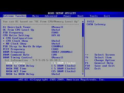
 The controller, called the EPU (Energy Processing Unit), is responsible for power management, thanks to which the manufacturer promises energy savings of up to 56.8% at low processor load. How true this is, and not another trick of marketers, one can only guess.
 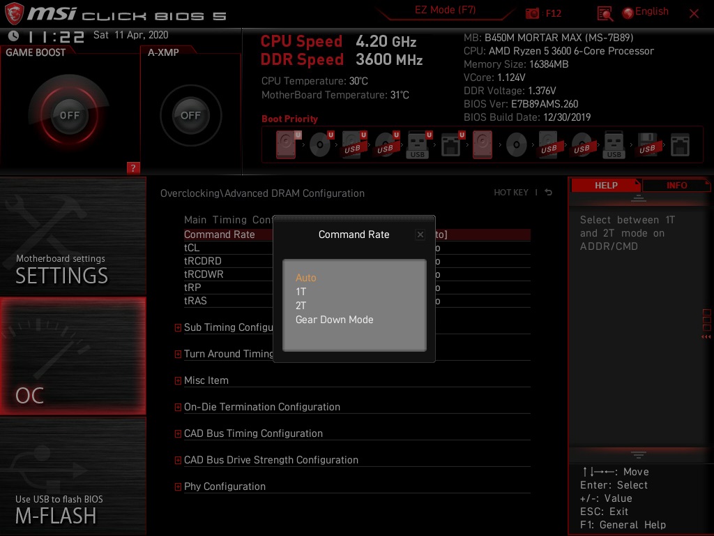 But no matter what the cooling system is, no matter what solid capacitors and chokes in armored cores are used, and the CPU power subsystem implementation scheme itself, everything can come to naught if there is only a conventional 4-pin ATX12V auxiliary power connector. And if this is quite enough for overclocking the Core 2 Duo, then, alas, this connector will not be enough to unlock the potential of a quad-core processor.
  The FrontPanel block, like on seven-year-old boards, without color coding, but with signatures, and the existing set of branded Q-Connector connectors will allow you to first connect the wires from the front panel to them, and then to the board. The ClearCMOS jumper is combined with the contacts of the case opening sensor and is located right next to the FrontPanel — you can’t do without tweezers here.
 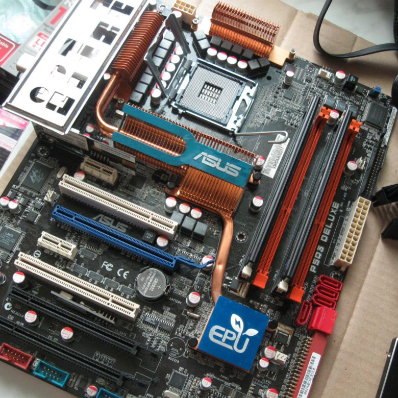 The 7.1-channel HAD codec Realtek ALC883 is used as an audio subsystem.
 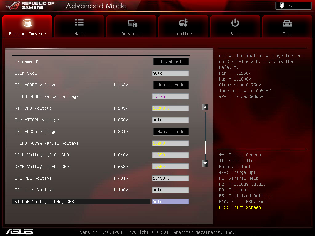 Such a system will be easily cooled by a mega-cooler with a horizontal fan, but with a tower-type cooler, you will have to resort to installing additional bundled fans, since the board has 6 fan connectors.
  For owners of «old» expansion cards, there are two PCI slots.
 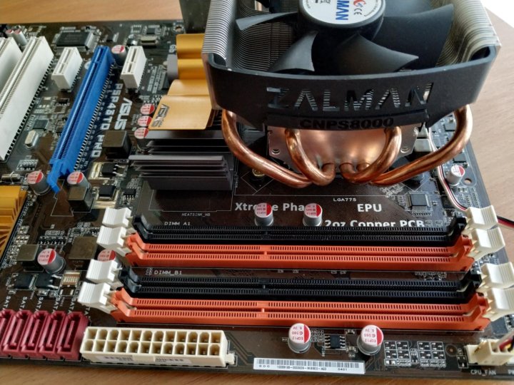 Naturally, this difference was reflected in the price — about 50-60 dollars.
 You can’t say the same about ASUS products — the delivery package is top notch as always, and the functionality corresponds to the price, which also depends on the positioning of the chipset. In this case, the cost of solutions based on Intel X38 will not be small by definition — the chipset itself is top-end, which means that boards based on it at a price of less than $200 will not appear soon. Unless after the release of the next flagship of Intel — X48, which will be officially presented this spring. Then yes, it will be possible to think about buying, and then for the sake of building a powerful CrossFire system, which with the Radeon HD 3870 is not so productive.
 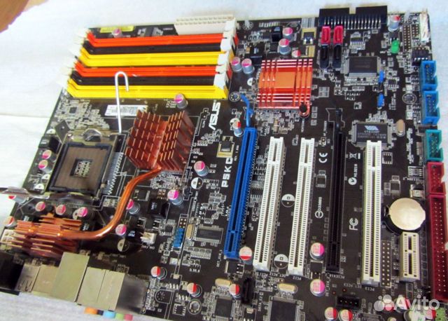 An interesting technology using the EPU, designed to save power at a low load on the processor, has not yet been run-in, so we won’t focus on it too much — there is, and that’s okay with it. The only negative in all this is the final cost of the finished system, because DDR3 memory modules are still quite expensive.